REVIEW 4 major objections 9 minor 130 references
Tunable Nanostructuring for van der Waals Materials
T0 review · 4 major / 9 minor · reviewed 2026-08-12 · deepseek-v4-flash
Pith's one-line read One femtosecond laser setup in a liquid turns more than fifty van der Waals precursors into stable, crystalline nanoparticles with shapes from spheres to nanocubes.
desk verdict A real breadth-first data set on fs-laser vdW nanoparticles, with an unproven universality claim that needs failure statistics before it can be taken at face value. read the letter →
The pith
A machine-rendered reading of the paper's core claim, the machinery that carries it, and where it could break.
The reading
What carries the argument
The central object is the femtosecond laser ablation and fragmentation-in-liquid process itself: focused fs pulses with intensity $>10^9$ W/cm$^2$ strike a bulk crystal or powder dispersed in acetonitrile, ejecting material that condenses through a plasma and cavitation bubble into colloidal nanoparticles. The fs pulse width is what preserves the parent crystal structure, because it minimizes thermal damage, and the liquid's confinement plus the supercontinuum generated in it let nearly any source material absorb the pulse energy. Fragmentation proceeds through Coulomb explosion and photothermal evaporation, while the choice of solvent adjusts particle size, oxidation state, and optical extinction. The argument is completed by molecular dynamics with machine-learned moment tensor potentials, which shows MoS2 droplets crystallize by competing surface-shell and bulk processes, so the cooling rate controls the shell-to-core ratio and crystallite size.
What would settle it
A concrete test would be to apply the exact acetonitrile protocol to a list of van der Waals materials selected without regard to ease of ablation—including air-sensitive MXenes, low-melting perovskites, and refractory chalcogenides—and count how many yield crystalline nanoparticles with the parent composition; if the success rate is materially below the reported set, the universality claim fails. A supporting quantitative check would report per-material morphology yields and failed syntheses, which the paper does not include.
Extended reading notes
Core claim
On its own terms, the paper establishes that one experimental protocol—pulsed femtosecond laser ablation of bulk crystals or fragmentation of powders in acetonitrile—turns van der Waals precursors into stable colloidal nanoparticles without bespoke chemistry per material. The authors report success on over fifty precursors spanning transition metal dichalcogenides, MXenes, perovskites, and related layered compounds, with detailed electron microscopy, diffraction, and EDX evidence for six representative cases: MoSe2, PtTe2, Ti3C2, HfS3, WTe2, and MAPbBr3. The nanoparticles keep the parent crystal structure and composition while appearing as nanospheres, fullerene-like polyhedra, faceted polygons, equilateral nanopyramids with a 7.5 nm step pitch, and nanocubes. Size is reported as a tunable outcome: changing the solvent moves MoS2 from roughly 75 nm in water to 42 nm in acetone to 15 nm in acetonitrile, and centrifugation separates size fractions. Molecular dynamics with machine-learned potentials attributes the internal structure to competing surface-shell and bulk crystallization during cooling, with the shell-to-core ratio set by cooling rate.
Load-bearing premise
The load-bearing premise is that the fifty-plus precursors shown are a fair sample of van der Waals materials as a class; no failed syntheses or per-material success rates are reported, so the claimed universality rests on the selection being representative.
Editorial extensions
If this is right
- A single setup can screen a library of van der Waals precursors: the same laser and solvent combination already produced nanoparticles from more than fifty materials, so adding a new candidate to the workflow requires no new chemistry.
- Solvent choice gives a straightforward size dial: reported MoS2 modes shift from 75 nm in water to 42 nm in acetone to 15 nm in acetonitrile, which translates directly into tuneable optical extinction.
- Because the nanoparticles keep the parent composition and crystallinity, their electronic and optical behavior should follow from the parent material, allowing the van der Waals family's known properties to be transferred to colloidal form.
- The cooling-rate dependence of the core-shell structure, seen in the molecular dynamics simulations, means laser parameters that change the thermal history can be used to engineer internal nanostructure and therefore optical response.
Reading between the lines
- The paper implicitly redefines the method as a discovery tool: if universality is real, a lab can ablate dozens of van der Waals materials in one session and generate a first map of which layered crystals form stable colloids, a resource that does not currently exist.
- The material-specific shapes (WTe2 nanopyramids, MAPbBr3 nanocubes, HfS3 polygons) hint that final morphology is partly inherited from the precursor's crystal habit, not solely controlled by laser parameters; this could be tested by ablating one material under widely varying solvents and pulse energies to see whether its shape family persists.
- A natural testable extension is to combine the demonstrated centrifugation size sorting with solvent tuning to produce monodisperse, shape-selected nanoparticle libraries and then measure application-relevant properties such as photothermal conversion or catalytic activity per shape; the paper's data make this feasible but do not demonstrate it.
Editorial analysis
A structured set of objections, weighed in public.
Referee Report
Summary. The manuscript reports that femtosecond pulsed laser ablation and fragmentation in liquids can produce stable colloidal nanoparticles (NPs) from a wide range of van der Waals (vdW) precursors, and claims this constitutes an express, universal nanostructuring method. Over 50 precursor materials are claimed, covering transition metal dichalcogenides, MXenes, perovskites, and other layered compounds, while the main text gives detailed TEM/HAADF/SAED/EDX characterization for six representative materials (MoSe2, PtTe2, Ti3C2, HfS3, WTe2, MAPbBr3). The NPs are reported to retain the composition and crystal structure of the initial materials while exhibiting diverse shapes ranging from spheres to fullerene-like polygons, nanopyramids, and nanocubes; solvent choice is shown to tune size (e.g., MoS2 NPs from 75 ± 41 nm in water to 15 ± 9 nm in acetonitrile). Machine-learned molecular dynamics of MoS2 melt crystallization predicts a core-shell polycrystal whose shell/core ratio depends on cooling rate, and the paper projects the approach to 'more than 5,000 members of the vdW family.'
Significance. If the universality claim is corroborated by full statistics, the result is a significant practical advance: a single laser-based protocol that could replace material-specific nanostructuring recipes for layered compounds, supported here by direct TEM, HAADF, SAED, and EDX evidence, reproducible synthesis parameters, and quantitative size distributions. The molecular dynamics uses a machine-learned moment tensor potential with explicit training-data error rather than ad hoc parameters, and no free parameters are fitted to the target experimental results, so the circularity concern raised in review does not land. The Discussion appropriately acknowledges scalability, recyclability, and stability as remaining challenges. The significance is nevertheless contingent: the 'over 50 materials' and 'universal' claims rest on the reported sample being representative, with defined success criteria, and that is exactly what is missing.
major comments (4)
- [The versatility of the laser ablation method for the synthesis of vdW NPs] The central claim of universality, based on 'over 50 materials' in the Abstract and Conclusions, is not supported by the evidence presented. Detailed characterization is given for only six materials (MoSe2, PtTe2, Ti3C2, HfS3, WTe2, MAPbBr3); the remaining ~44 precursors appear only in Figure S1 and Table S1, which are not included in the manuscript text as provided. No denominator is reported: the number of precursors attempted, the number of failed syntheses, the per-material success criterion (colloid stability, crystallinity, or shape yield), and the fraction of particles per sample displaying the claimed 'well-defined' geometry are all absent. Without these data, the claim cannot be distinguished from a curated selection of favorable cases, and the extrapolation to 'more than 5,000 members of the vdW family' (Introduction, Conclusions) is unsupported. Please provide a complete per-material table with the synthesis route (ablation vs fragmentation), outcome, yield, morphology distribution, and the corresponding SI data, and calibrate the wording to what is demonstrated.
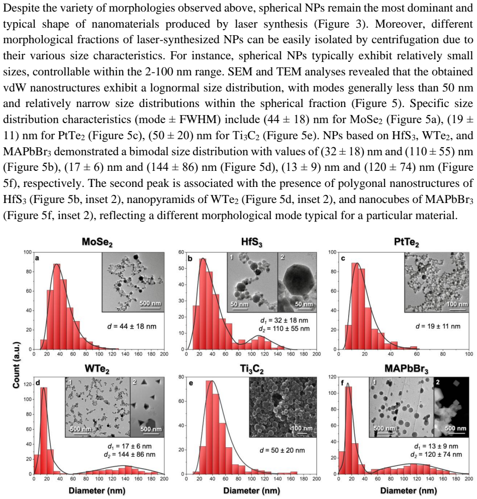
- [Morphology and structure of vdW NPs (Figure 5)] The claim of tunable shape ('from nanospheres to nanocubes and nanotetrahedrons', Abstract) is unquantified. The text states that 'spherical NPs remain the most dominant and typical shape', and for HfS3, WTe2, and MAPbBr3, Figure 5 shows bimodal size distributions in which the non-spherical fraction (polygons, pyramids, cubes) appears as a second, minority peak (e.g., (17 ± 6) nm vs (144 ± 86) nm for WTe2). The fraction of particles in the shape-specific population is not reported, nor is any quantitative criterion for 'well-defined geometry' given. In addition, the size distributions are obtained with an ImageJ 'circle fit approximation' (Methods), which is not a well-defined metric for anisotropic particles such as 180 nm nanopyramids with a 7.5 nm step pitch. Please report per-morphology yields and adopt shape-appropriate size metrics (e.g., edge length for cubes and pyramids).
- [Morphology and structure of vdW NPs] There is an internal tension in the structure-preservation claim. The text asserts that NPs 'retain crystallographic planes and chemical compositions corresponding to the initial materials' and the Conclusions claim 'maintaining the original crystalline structure of over 50 vdW materials', yet two paragraphs later it reports that MoSe2 and PtTe2 NPs have 'unique interplanar distances in their crystalline shells, which differ from those of the initial materials'. As written, the abstract claim of 'perfectly defined crystalline structures' is not quantitatively defined: what deviation in interplanar spacing, and in what fraction of the particle, is still considered 'corresponding to the initial material'? Please specify the tolerance and give measured versus bulk d-spacings for each detailed material, including the 6.4 Å shell spacing of HfS3 and the 2.6 Å spacing of Ti3C2.
- [Laser-driven synthesis of vdW NPs (Figure 2b, Figures S3-S4)] The MD simulations of MoS2 melt crystallization are used to claim that 'the cooling process can modulate the nanostructure parameters of NPs and their optical properties'. However, the modeled cooling rates (0.08-2 K/ns) are not tied to any experimental control or measurement in the laser ablation or fragmentation setup, and no quantitative comparison is made between the MD-predicted shell thickness, inner crystallite size, or their cooling-rate dependence and the TEM observations. As presented, the MD is illustrative rather than validated mechanistic support. Please add a quantitative MD-experiment comparison (e.g., for MoS2 or MoSe2 NPs) or explicitly soften the claim to state that the simulations suggest a cooling-rate dependence that is not yet experimentally verified.
minor comments (9)
- [Abstract] The phrase 'disarming simplicity' is informal for a journal article; suggest 'remarkable simplicity' or similar.
- [Figure 5] Clarify which panels are SEM and which are TEM; the caption says 'TEM/SEM image', but the Methods state that size distributions were measured from SEM images by circle fitting while the text refers to TEM images.
- [Methods (Molecular dynamics)] The MTP accuracy is quoted as the error on the training data (16 meV/atom); please also report the prediction error on validation configurations held out during the active-learning iterations, since the training error alone can be overly optimistic.
- [Figure 6] The pie chart is said to be based on 'an analysis of over 3,000 scholarly articles', but no methodology, search terms, or citation are given; please specify the analysis or move the figure to the SI with a description.
- [Data Availability] The datasets are 'available from the corresponding author upon reasonable request', but the manuscript cites Figures S1-S4 and Table S1 without including them in the provided text; please deposit the SI and, ideally, the raw TEM/SAED data in a public repository.
- [Morphology and structure of vdW NPs] The term 'unique interplanar distances' should be replaced with the measured values and a comparison with the bulk lattice parameters, as the current wording is imprecise.
- [Introduction] References [45] and [60] are the authors' own prior work on MoS2 NPs; the novelty of the present contribution relative to those works should be stated explicitly in the introduction.
- [The versatility of the laser ablation method for the synthesis of vdW NPs] The zeta-potential validation of colloidal stability (Figure S2d) is mentioned but no typical values are given in the text; please report representative zeta-potentials.
- [Discussion] Subscript formatting is inconsistent (e.g., 'WS₂', 'Ta₂C', and 'Cu2-xS' alongside 'MoS2'); please unify the formatting throughout the text.
Circularity Check
No circular derivation: the universality claim rests on independent TEM/SAED/EDX observations, and the few self-citations are motivational rather than load-bearing.
full rationale
The paper's core claim—that femtosecond laser ablation and fragmentation yield stable, crystalline, shape-diverse vdW nanoparticles from more than 50 precursors—is an experimental generalization supported by direct TEM, HAADF, SAED, and EDX characterization rather than by a fitted model or by equations that define the outcome in terms of the inputs. Detailed microscopy is reported for MoSe2, PtTe2, Ti3C2, HfS3, WTe2, and MAPbBr3, with the remaining materials summarized in the SI; nothing in the main text reduces a 'prediction' to a fitted parameter or to a self-citation. The MD portion uses a machine-learned MTP fitted to DFT energies and forces, and the resulting core-shell crystallization mechanism is an independent simulation output, not an input assumed to produce the claimed universality. Self-citations to the authors' prior work (refs 45, 60, 122, 123) establish the starting ablation/fragmentation protocol and earlier MoS2 size-separation results; these are motivational and methodological, not the evidence for the 50+ material claim. Thus no circular step can be quoted from the paper's equations or logic. Possible weaknesses—lack of per-material success rates, selection-bias in the reported 50+ list, and internal tension in interplanar-distance claims—are correctness and evidence concerns, not circularity.
Assumptions & free parameters
assumptions (3)
- domain assumption Femtosecond laser ablation and fragmentation preserve the crystalline structure and chemical composition of the precursor vdW material.
- domain assumption The machine-learned MTP potential trained on 3,250 Mo-S configurations extrapolates reliably to MoS2 melt crystallization at 0.08-2 K/ns cooling rates.
- domain assumption Acetonitrile prevents significant oxidation and preserves composition of the synthesized NPs.
Cite this review
Pith. "Pith review of Tunable Nanostructuring for van der Waals Materials." pith.science (2026). https://pith.science/paper/OJCG3QR2
@misc{pith2026241114060,
  author       = {Pith},
  title        = {Pith review of: Tunable Nanostructuring for van der Waals Materials},
  year         = {2026},
  howpublished = {\url{https://pith.science/paper/OJCG3QR2}},
  note         = {Machine review of arXiv:2411.14060}
}
read the original abstract
Van der Waals (vdW) materials are becoming increasingly popular in scientific and industrial applications because of their unique mixture of record electronic, optical, and mechanical properties. However, nanostructuring of vdW materials is still in its infancy and strongly depends on the specific vdW crystal. As a result, the universal self-assembled technology of vdW materials nanostructuring opens vast technological prospects. This work demonstrates an express and universal synthesis method of vdW nanoparticles with well-defined geometry using femtosecond laser ablation and fragmentation. The disarming simplicity of the technique allows us to create nanoparticles from over 50 vdW precursor materials covering transition metal chalcogenides, MXenes, and other vdW materials. Obtained nanoparticles manifest perfectly defined crystalline structures and diverse shapes, from nanospheres to nanocubes and nanotetrahedrons. Thus, our work provides a new paradigm for vdW nanostructuring with a vast potential of tunability for size, shape, and materials specific to the particular application.
Figures


Figures from the paper (3 more)


Reference graph
Works this paper leans on
-
[1]
Q. H. Wang, K. Kalantar -Zadeh, A. Kis, J. N. Coleman, M. S. Strano, Nat. Nanotechnol. 2012, 7, 699
2012
-
[2]
Mueller, E
T. Mueller, E. Malic, Npj 2D Mater. Appl. 2018, 2, 1
2018
-
[3]
H. Park, M. Lee, X. Wang, N. Ali, K. Watanabe, T. Taniguchi, E. Hwang, W. J. Yoo, Commun. Mater. 2024, 5, 1
2024
-
[4]
Liang, B
S. Liang, B. Cheng, X. Cui, F. Miao, Adv. Mater. 2020, 32, 1903800
2020
-
[5]
K. S. Burch, D. Mandrus, J.-G. Park, Nature 2018, 563, 47
2018
-
[6]
Q. H. Wang, A. Bedoya-Pinto, M. Blei, A. H. Dismukes, A. Hamo, S. Jenkins, M. Koperski, Y. Liu, Q.-C. Sun, E. J. Telford, H. H. Kim, M. Augustin, U. Vool, J. -X. Yin, L. H. Li, A. Falin, C. R. Dean, F. Casanova, R. F. L. Evans, M. Chshiev, A. Mishchenko , C. Petrovic, R. He, L. Zhao, A. W. Tsen, B. D. Gerardot, M. Brotons -Gisbert, Z. Guguchia, X. Roy, S....
2022
-
[7]
J. T. Gish, D. Lebedev, T. W. Song, V. K. Sangwan, M. C. Hersam, Nat. Electron. 2024, 1
2024
-
[8]
A. K. Geim, I. V. Grigorieva, Nature 2013, 499, 419
2013
Show all 130 references
-
[9]
K. S. Novoselov, A. Mishchenko, A. Carvalho, A. H. Castro Neto, Science 2016, 353, aac9439
2016
-
[10]
J.-H. Fu, A. -Y. Lu, N. J. Madden, C. C. Wu, Y. -C. Chen, M. -H. Chiu, K. Hattar, J. A. Krogstad, S. S. Chou, L.-J. Li, J. Kong, V. Tung, Commun. Mater. 2020, 1, 1
2020
-
[11]
D. Hu, X. Yang, C. Li, R. Liu, Z. Yao, H. Hu, S. N. G. Corder, J. Chen, Z. Sun, M. Liu, Q. Dai, Nat. Commun. 2017, 8, 1471
2017
-
[12]
G. A. Ermolaev, D. V. Grudinin, Y. V. Stebunov, K. V. Voronin, V. G. Kravets, J. Duan, A. B. Mazitov, G. I. Tselikov, A. Bylinkin, D. I. Yakubovsky, S. M. Novikov, D. G. Baranov, A. Y. Nikitin, I. A. Kruglov, T. Shegai, P. Alonso -González, A. N. Grigo renko, A. V. Arsenin, K....
2021
-
[13]
Mooshammer, S
F. Mooshammer, S. Chae, S. Zhang, Y. Shao, S. Qiu, A. Rajendran, A. J. Sternbach, D. J. Rizzo, X. Zhu, P. J. Schuck, J. C. Hone, D. N. Basov, ACS Photonics 2022, 9, 443
2022
-
[14]
A. A. Vyshnevyy, G. A. Ermolaev, D. V. Grudinin, K. V. Voronin, I. Kharichkin, A. Mazitov, I. A. Kruglov, D. I. Yakubovsky, P. Mishra, R. V. Kirtaev, A. V. Arsenin, K. S. Novoselov, L. Martin-Moreno, V. S. Volkov, Nano Lett. 2023, 23, 8057
2023
-
[15]
Y. Meng, J. Feng, S. Han, Z. Xu, W. Mao, T. Zhang, J. S. Kim, I. Roh, Y. Zhao, D.-H. Kim, Y. Yang, J.-W. Lee, L. Yang, C.-W. Qiu, S.-H. Bae, Nat. Rev. Mater. 2023, 8, 498
2023
-
[16]
Verre, D
R. Verre, D. G. Baranov, B. Munkhbat, J. Cuadra, M. Käll, T. Shegai, Nat. Nanotechnol. 2019, 14, 679
2019
-
[17]
Flöry, P
N. Flöry, P. Ma, Y. Salamin, A. Emboras, T. Taniguchi, K. Watanabe, J. Leuthold, L. Novotny, Nat. Nanotechnol. 2020, 15, 118
2020
-
[18]
H. Ling, J. B. Khurgin, A. R. Davoyan, Nano Lett. 2022, 22, 6254
2022
-
[19]
D. A. Bandurin, E. Mönch, K. Kapralov, I. Y. Phinney, K. Lindner, S. Liu, J. H. Edgar, I. A. Dmitriev, P. Jarillo-Herrero, D. Svintsov, S. D. Ganichev, Nat. Phys. 2022, 18, 462
2022
-
[20]
Anasori, M
B. Anasori, M. R. Lukatskaya, Y. Gogotsi, Nat. Rev. Mater. 2017, 2, 1
2017
-
[21]
Chaves, J
A. Chaves, J. G. Azadani, H. Alsalman, D. R. da Costa, R. Frisenda, A. J. Chaves, S. H. Song, Y. D. Kim, D. He, J. Zhou, A. Castellanos-Gomez, F. M. Peeters, Z. Liu, C. L. Hinkle, S.-H. Oh, P. D. Ye, S. J. Koester, Y. H. Lee, P. Avouris, X. Wang, T. L ow, Npj 2D Mater. Appl. 2...
2020
-
[22]
C. R. Dean, A. F. Young, I. Meric, C. Lee, L. Wang, S. Sorgenfrei, K. Watanabe, T. Taniguchi, P. Kim, K. L. Shepard, J. Hone, Nat. Nanotechnol. 2010, 5, 722
2010
-
[23]
O. Song, D. Rhee, J. Kim, Y. Jeon, V. Mazánek, A. Söll, Y. A. Kwon, J. H. Cho, Y. -H. Kim, Z. Sofer, J. Kang, Npj 2D Mater. Appl. 2022, 6, 1
2022
-
[24]
Y. Shao, L. Wei, X. Wu, C. Jiang, Y. Yao, B. Peng, H. Chen, J. Huangfu, Y. Ying, C. J. Zhang, J. Ping, Nat. Commun. 2022, 13, 3223
2022
-
[25]
L. Sun, G. Yuan, L. Gao, J. Yang, M. Chhowalla, M. H. Gharahcheshmeh, K. K. Gleason, Y. S. Choi, B. H. Hong, Z. Liu, Nat. Rev. Methods Primer 2021, 1, 1
2021
-
[26]
A. V. Kabashin, Ph. Delaporte, A. Pereira, D. Grojo, R. Torres, Th. Sarnet, M. Sentis, Nanoscale Res. Lett. 2010, 5, 454
2010
-
[27]
Castellanos-Gomez, M
A. Castellanos-Gomez, M. Barkelid, A. M. Goossens, V. E. Calado, H. S. J. van der Zant, G. A. Steele, Nano Lett. 2012, 12, 3187
2012
-
[28]
Mupparapu, M
R. Mupparapu, M. Steinert, A. George, Z. Tang, A. Turchanin, T. Pertsch, I. Staude, Adv. Mater. Interfaces 2020, 7, 2000858
2020
-
[29]
Munkhbat, A
B. Munkhbat, A. B. Yankovich, D. G. Baranov, R. Verre, E. Olsson, T. O. Shegai, Nat. Commun. 2020, 11, 4604
2020
-
[30]
A. V. Kabashin, M. Meunier, J. Appl. Phys. 2003, 94, 7941
2003
-
[31]
I. B. Belyaev, I. V. Zelepukin, P. A. Kotelnikova, G. V. Tikhonowski, A. A. Popov, A. Yu. Kapitannikova, J. Barman, A. N. Kopylov, D. N. Bratashov, E. S. Prikhozhdenko, A. V. Kabashin, S. M. Deyev, A. V. Zvyagin, Adv. Sci. 2024, 11, 2307060
2024
-
[32]
N. G. Semaltianos, S. Logothetidis, W. Perrie, S. Romani, R. J. Potter, M. Sharp, P. French, G. Dearden, K. G. Watkins, Appl. Phys. A 2009, 94, 641
2009
-
[33]
C. L. Sajti, R. Sattari, B. N. Chichkov, S. Barcikowski, J. Phys. Chem. C 2010, 114, 2421
2010
-
[34]
Nolte, C
S. Nolte, C. Momma, H. Jacobs, A. Tünnermann, B. N. Chichkov, B. Wellegehausen, H. Welling, J. Opt. Soc. Am. B 1997, 14, 2716
1997
-
[35]
Mafuné, J
F. Mafuné, J. Kohno, Y. Takeda, T. Kondow, H. Sawabe, J. Phys. Chem. B 2000, 104, 9111
2000
-
[36]
Rehbock, V
C. Rehbock, V. Merk, L. Gamrad, R. Streubel, S. Barcikowski, Phys Chem Chem Phys 2013, 15, 3057
2013
-
[37]
Besner, A
S. Besner, A. V. Kabashin, M. Meunier, Appl. Phys. A 2007, 88, 269
2007
-
[38]
Zhang, B
D. Zhang, B. Gökce, S. Barcikowski, Chem. Rev. 2017, 117, 3990
2017
-
[39]
Sylvestre, A
J.-P. Sylvestre, A. V. Kabashin, E. Sacher, M. Meunier, J. H. T. Luong, J. Am. Chem. Soc. 2004, 126, 7176
2004
-
[40]
Amendola, M
V. Amendola, M. Meneghetti, Phys. Chem. Chem. Phys. 2009, 11, 3805
2009
-
[41]
Maximova, A
K. Maximova, A. Aristov, M. Sentis, A. V. Kabashin, Nanotechnology 2015, 26, 065601
2015
-
[42]
Sylvestre, S
J.-P. Sylvestre, S. Poulin, A. V. Kabashin, E. Sacher, M. Meunier, J. H. T. Luong, J. Phys. Chem. B 2004, 108, 16864
2004
-
[43]
Bärsch, J
N. Bärsch, J. Jakobi, S. Weiler, S. Barcikowski, Nanotechnology 2009, 20, 445603
2009
-
[44]
Streubel, S
R. Streubel, S. Barcikowski, B. Gökce, Opt. Lett. 2016, 41, 1486
2016
-
[45]
G. I. Tselikov, G. A. Ermolaev, A. A. Popov, G. V. Tikhonowski, D. A. Panova, A. S. Taradin, A. A. Vyshnevyy, A. V. Syuy, S. M. Klimentov, S. M. Novikov, A. B. Evlyukhin, A. V. Kabashin, A. V. Arsenin, K. S. Novoselov, V. S. Volkov, Proc. Natl. Acad. Sci. 2022, 119, e2208830119
2022
-
[46]
Kögler, Y
M. Kögler, Y. V. Ryabchikov, S. Uusitalo, A. Popov, A. Popov, G. Tselikov, A. Välimaa, A. Al‐Kattan, J. Hiltunen, R. Laitinen, P. Neubauer, I. Meglinski, A. V. Kabashin, J. Biophotonics 2018, 11, e201700225
2018
-
[47]
I. V. Zelepukin, A. A. Popov, V. O. Shipunova, G. V. Tikhonowski, A. B. Mirkasymov, E. A. Popova-Kuznetsova, S. M. Klimentov, A. V. Kabashin, S. M. Deyev, Mater. Sci. Eng. C 2021, 120, 111717
2021
-
[48]
Zhang, M
J. Zhang, M. Chaker, D. Ma, J. Colloid Interface Sci. 2017, 489, 138
2017
-
[49]
Farooq, C
S. Farooq, C. V. P. Vital, G. Tikhonowski, A. A. Popov, S. M. Klimentov, L. A.G. Malagon, R. E. De Araujo, A. V. Kabashin, D. Rativa, Sol. Energy Mater. Sol. Cells 2023, 252, 112203
2023
-
[50]
A. A. Popov, G. Tselikov, N. Dumas, C. Berard, K. Metwally, N. Jones, A. Al -Kattan, B. Larrat, D. Braguer, S. Mensah, A. Da Silva, M.-A. Estève, A. V. Kabashin, Sci. Rep. 2019, 9, 1194
2019
-
[51]
A. V. Kabashin, M. Meunier, C. Kingston, J. H. T. Luong, J. Phys. Chem. B 2003, 107, 4527
2003
-
[52]
Intartaglia, K
R. Intartaglia, K. Bagga, M. Scotto, A. Diaspro, F. Brandi, Opt. Mater. Express 2012, 2, 510
2012
-
[53]
Ibrahimkutty, P
S. Ibrahimkutty, P. Wagener, A. Menzel, A. Plech, S. Barcikowski, Appl. Phys. Lett. 2012, 101, 103104
2012
-
[54]
Al -Kattan, G
A. Al -Kattan, G. Tselikov, K. Metwally, A. A. Popov, S. Mensah, A. V. Kabashin, Nanomaterials 2021, 11, 592
2021
-
[55]
H. J. Jung, M. Y. Choi, J. Phys. Chem. C 2014, 118, 14647
2014
-
[56]
Blandin, K
P. Blandin, K. A. Maximova, M. B. Gongalsky, J. F. Sanchez -Royo, V. S. Chirvony, M. Sentis, V. Yu. Timoshenko, A. V. Kabashin, J. Mater. Chem. B 2013, 1, 2489
2013
-
[57]
Chichkov, Appl
B. Chichkov, Appl. Phys. A 2022, 128, 1015
2022
-
[58]
I. S. Novikov, K. Gubaev, E. V. Podryabinkin, A. V. Shapeev, Mach. Learn. Sci. Technol. 2021, 2, 025002
2021
-
[59]
A. V. Shapeev, Multiscale Model. Simul. 2016, 14, 1153
2016
-
[60]
A. S. Chernikov, G. I. Tselikov, M. Yu. Gubin, A. V. Shesterikov, K. S. Khorkov, A. V. Syuy, G. A. Ermolaev, I. S. Kazantsev, R. I. Romanov, A. M. Markeev, A. A. Popov, G. V. Tikhonowski, O. O. Kapitanova, D. A. Kochuev, A. Yu. Leksin, D. I. Tselikov, A. V. Arsenin, A. V. Kaba...
2023
-
[61]
Monga, S
D. Monga, S. Sharma, N. P. Shetti, S. Basu, K. R. Reddy, T. M. Aminabhavi, Mater. Today Chem. 2021, 19, 100399
2021
-
[62]
Sharma, S
S. Sharma, S. Basu, Sep. Purif. Technol. 2020, 231, 115916
2020
-
[63]
Fujishima, K
A. Fujishima, K. Honda, Nature 1972, 238, 37
1972
-
[64]
Mehta, A
A. Mehta, A. Mishra, S. Basu, N. P. Shetti, K. R. Reddy, T. A. Saleh, T. M. Aminabhavi, J. Environ. Manage. 2019, 250, 109486
2019
-
[65]
Monga, D
D. Monga, D. Ilager, N. P. Shetti, S. Basu, T. M. Aminabhavi, J. Environ. Manage. 2020, 274, 111208
2020
-
[66]
G. A. Ermolaev, Y. V. Stebunov, A. A. Vyshnevyy, D. E. Tatarkin, D. I. Yakubovsky, S. M. Novikov, D. G. Baranov, T. Shegai, A. Y. Nikitin, A. V. Arsenin, V. S. Volkov, Npj 2D Mater. Appl. 2020, 4, 21
2020
-
[67]
Y. Li, H. Wang, L. Xie, Y. Liang, G. Hong, H. Dai, J. Am. Chem. Soc. 2011, 133, 7296
2011
-
[68]
A. F. Ismail, P. S. Goh, H. Hasbullah, F. Aziz, Advanced Materials for Wastewater Treatment and Desalination: Fundamentals to Applications, CRC Press, Boca Raton, 2022
2022
-
[69]
Kalantar-Zadeh, J
K. Kalantar-Zadeh, J. Z. Ou, ACS Sens. 2016, 1, 5
2016
-
[70]
H. J. Kim, J. H. Lee, Sens. Actuators B Chem. 2014, 192, 607
2014
-
[71]
Joshi, T
N. Joshi, T. Hayasaka, Y. Liu, H. Liu, O. N. Oliveira, L. Lin, Microchim. Acta 2018, 185, 213
2018
-
[72]
Presutti, T
D. Presutti, T. Agarwal, A. Zarepour, N. Celikkin, S. Hooshmand, C. Nayak, M. Ghomi, A. Zarrabi, M. Costantini, B. Behera, T. K. Maiti, Materials 2022, 15, 337
2022
-
[73]
Goswami, G
P. Goswami, G. Gupta, Mater. Today Chem. 2022, 23, 100726
2022
-
[74]
X. Liu, H. L. Shuai, Y. J. Liu, K. J. Huang, Sens. Actuators B Chem. 2016, 235, 603
2016
-
[75]
K. J. Huang, Y. J. Liu, J. T. Cao, H. B. Wang, RSC Adv. 2014, 4, 36742
2014
-
[76]
K. J. Huang, H. L. Shuai, J. Z. Zhang, Biosens. Bioelectron. 2016, 77, 69
2016
-
[77]
Jariwala, S
D. Jariwala, S. L. Howell, K. S. Chen, J. Kang, V. K. Sangwan, S. A. Filippone, R. Turrisi, T. J. Marks, L. J. Lauhon, M. C. Hersam, Nano Lett. 2016, 16, 497
2016
-
[78]
Jiang, D
H. Jiang, D. Ren, H. Wang, Y. Hu, S. Guo, H. Yuan, P. Hu, L. Zhang, C. Li, Adv. Mater. 2015, 27, 3687
2015
-
[79]
C. Zhao, J. Kong, X. Yao, X. Tang, Y. Dong, S. L. Phua, X. Lu, ACS Appl. Mater. Interfaces 2014, 6, 6392
2014
-
[80]
Kumar, D
N. Kumar, D. Mishra, A. Kumar, B. Dash, R. K. Mishra, J. Song, S. H. Jin, Appl. Sci. Switz. 2023, 13, 3678
2023
-
[81]
S. K. Park, S. H. Yu, S. Woo, B. Quan, D. C. Lee, M. K. Kim, Y. E. Sung, Y. Piao, J. Chem. Soc. Dalton Trans. 2013, 42, 2399
2013
-
[82]
Z. Wang, H. Wu, G. W. Burr, C. S. Hwang, K. L. Wang, Q. Xia, J. J. Yang, Nat. Rev. Mater. 2020, 5, 173
2020
-
[83]
J. Tang, F. Yuan, X. Shen, Z. Wang, M. Rao, Y. He, Y. Sun, X. Li, W. Zhang, Y. Li, B. Gao, H. Qian, G. Bi, S. Song, J. J. Yang, H. Wu, Adv. Mater. 2019, 31, DOI 10.1002/adma.201902761
2019 doi
-
[84]
M. K. Song, J. H. Kang, X. Zhang, W. Ji, A. Ascoli, I. Messaris, A. S. Demirkol, B. Dong, S. Aggarwal, W. Wan, S. M. Hong, S. G. Cardwell, I. Boybat, J. S. Seo, J. S. Lee, M. Lanza, H. Yeon, M. Onen, J. Li, B. Yildiz, J. A. del Alamo, S. Kim, S. Choi, G. Milano, C. Ricciardi, ...
2023
-
[85]
P. Liu, H. Luo, X. Yin, X. Wang, X. He, J. Zhu, H. Xue, W. Mao, Y. Pu, Appl. Phys. Lett. 2022, 121, DOI 10.1063/5.0127880
2022 doi
-
[86]
Zhang, H
X. Zhang, H. Qiao, X. Nian, Y. Huang, X. Pang, J. Mater. Sci. Mater. Electron. 2016, 27, 7609
2016
-
[87]
Y. Yan, B. Sun, D. Ma, Chem. Phys. Lett. 2015, 638, 103
2015
-
[88]
P. Li, B. Sun, X. Zhang, G. Zhou, Y. Xia, L. Gan, Y. Zhang, Y. Zhao, Mater. Lett. 2017, 202, 13
2017
-
[89]
Jamilpanah, I
L. Jamilpanah, I. Khademi, J. Shoa e Gharehbagh, S. Aziz Mohseni, S. M. Mohseni, J. Alloys Compd. 2020, 835, 155291
2020
-
[90]
R. Kaur, K. P. Singh, S. K. Tripathi, J. Alloys Compd. 2022, 905, 164103
2022
-
[91]
R. Kaur, K. P. Singh, S. K. Tripathi, J. Mater. Sci. Mater. Electron. 2020, 31, 19974
2020
-
[92]
Y. Li, J. Cao, J. Chen, Q. Xu, X. Liu, J. Qiu, Y. Chen, H. Wang, M. Wang, IEEE Electron Device Lett. 2023, 44, 2047
2023
-
[93]
M. E. Pereira, R. Martins, E. Fortunato, P. Barquinha, A. Kiazadeh, Neuromorphic Comput. Eng. 2023, 3, 022002
2023
-
[94]
Y. Zhai, X. Yang, F. Wang, Z. Li, G. Ding, Z. Qiu, Y. Wang, Y. Zhou, S. T. Han, Adv. Mater. 2018, 30, DOI 10.1002/adma.201803563
2018 doi
-
[95]
Y. Tian, S. Zhang, W. Tan, Appl. Nanosci. Switz. 2022, 12, 2023
2022
-
[96]
M. Chen, S. J. Ki, X. Liang, ACS Appl. Electron. Mater. 2023, 5, 3830
2023
-
[97]
E. A. Konstantinova, A. A. Minnekhanov, G. V. Trusov, V. G. Kytin, Nanotechnology 2020, 31, 345207
2020
-
[98]
J. Xia, Y. Ge, D. Zhao, J. Di, M. Ji, S. Yin, H. Li, R. Chen, CrystEngComm 2015, 17, 3645
2015
-
[99]
X. Zou, J. Zhang, X. Zhao, Z. Zhang, Chem. Eng. J. 2020, 383, 123084
2020
-
[100]
Q. Li, N. Zhang, Y. Yang, G. Wang, D. H. L. Ng, Langmuir 2014, 30, 8965
2014
-
[101]
H. Chen, T. Liu, Z. Su, L. Shang, G. Wei, Nanoscale Horiz. 2018, 3, 74
2018
-
[102]
Cheng, J
L. Cheng, J. Liu, X. Gu, H. Gong, X. Shi, T. Liu, C. Wang, X. Wang, G. Liu, H. Xing, W. Bu, B. Sun, Z. Liu, Adv. Mater. 2014, 26, 1886
2014
-
[103]
D. An, J. Fu, B. Zhang, N. Xie, G. Nie, H. Ågren, M. Qiu, H. Zhang, Adv. Funct. Mater. 2021, 31, 2101625
2021
-
[104]
D. Xu, Z. Li, L. Li, J. Wang, Adv. Funct. Mater. 2020, 30, 2000712
2020
-
[105]
Y. Zhao, B. -Q. Chen, R. K. Kankala, S. -B. Wang, A. -Z. Chen, ACS Biomater. Sci. Eng. 2020, 6, 4799
2020
-
[106]
G. Liu, J. Zou, Q. Tang, X. Yang, Y. Zhang, Q. Zhang, W. Huang, P. Chen, J. Shao, X. Dong, ACS Appl. Mater. Interfaces 2017, 9, 40077
2017
-
[107]
Zhang, X
H. Zhang, X. Zeng, Z. Li, ACS Appl. Bio Mater. 2020, 3, 6529
2020
-
[108]
X. Song, Q. Huang, Y. Yang, L. Ma, W. Liu, C. Ou, Q. Chen, T. Zhao, Z. Xiao, M. Wang, Y. Jiang, Y. Yang, J. Zhang, Y. Nan, W. Wu, K. Ai, Adv. Mater. 2023, 35, 2301585
2023
-
[109]
J. Shao, J. Zhang, C. Jiang, J. Lin, P. Huang, Chem. Eng. J. 2020, 400, 126009
2020
-
[110]
X. Han, J. Huang, H. Lin, Z. Wang, P. Li, Y. Chen, Adv. Healthc. Mater. 2018, 7, 1701394
2018
-
[111]
Valencia, C
C. Valencia, C. H. Valencia, F. Zuluaga, M. E. Valencia, J. H. Mina, C. D. Grande -Tovar, Molecules 2018, 23, 2651
2018
-
[112]
Silva, I
M. Silva, I. S. Pinho, J. A. Covas, N. M. Alves, M. C. Paiva, Funct. Compos. Mater. 2021, 2, 8
2021
-
[113]
P. G. Zotev, Y. Wang, D. Andres‐Penares, T. Severs‐Millard, S. Randerson, X. Hu, L. Sortino, C. Louca, M. Brotons‐Gisbert, T. Huq, S. Vezzoli, R. Sapienza, T. F. Krauss, B. D. Gerardot, A. I. Tartakovskii, Laser Photonics Rev. 2023, 17, 2200957
2023
-
[114]
M. R. Jobayr, E. M. T. Salman, Chin. J. Phys. 2021, 74, 270
2021
-
[115]
W. Y. Lee, M. S. Kang, J. W. Choi, S. H. Kim, N. W. Park, G. S. Kim, Y. H. Kim, S. K. Lee, Adv. Electron. Mater. 2023, 9, DOI 10.1002/aelm.202300170
2023 doi
-
[116]
D. Qin, P. Yan, G. Ding, X. Ge, H. Song, G. Gao, Sci. Rep. 2018, 8, 2764
2018
-
[117]
Zhang, H
J. Zhang, H. J. Liu, L. Cheng, J. Wei, J. H. Liang, D. D. Fan, J. Shi, X. F. Tang, Q. J. Zhang, Sci. Rep. 2014, 4, 6452
2014
- [118]
-
[119]
Tarachand, G. S. Okram, B. K. De, S. Dam, S. Hussain, V. Sathe, U. Deshpande, A. Lakhani, Y. K. Kuo, ACS Appl. Mater. Interfaces 2020, 12, 37248
2020
-
[120]
Y. X. Zhang, Y. K. Zhu, D. S. Song, J. Feng, Z. H. Ge, Chem. Commun. 2021, 57, 2555
2021
-
[121]
Y. Zhou, N. Li, Y. Xin, X. Cao, S. Ji, P. Jin, J. Mater. Chem. C 2017, 5, 6251
2017
-
[122]
J. C. Bulmahn, G. Tikhonowski, A. A. Popov, A. Kuzmin, S. M. Klimentov, A. V. Kabashin, P. N. Prasad, Nanomaterials 2020, 10, 1463
2020
-
[123]
A. Hahn, J. Laser MicroNanoengineering 2008, 3, 73
2008
-
[124]
Popov, G
A. Popov, G. Tikhonowski, P. Shakhov, E. Popova-Kuznetsova, G. Tselikov, R. Romanov, A. Markeev, S. Klimentov, A. Kabashin, Nanomaterials 2022, 12, 1672
2022
-
[125]
Plimpton, J
S. Plimpton, J. Comput. Phys. 1995, 117, 1
1995
-
[126]
D. J. Evans, B. L. Holian, J. Chem. Phys. 1985, 83, 4069
1985
-
[127]
Kresse, D
G. Kresse, D. Joubert, Phys. Rev. B 1999, 59, 1758
1999
-
[128]
J. P. Perdew, K. Burke, M. Ernzerhof, Phys. Rev. Lett. 1996, 77, 3865
1996
-
[129]
P. E. Blöchl, Phys. Rev. B 1994, 50, 17953
1994
-
[130]
Grimme, J
S. Grimme, J. Antony, S. Ehrlich, H. Krieg, J. Chem. Phys. 2010, 132, 154104
2010
Reviewed August 12, 2026 · model on record in the stance chip above.
Discussion (0). Continue with ORCID to comment.