REVIEW 4 major objections 5 minor 11 references
Scaling mixed-signal neuromorphic processors to 28 nm FD-SOI technologies
T0 review · 4 major / 5 minor · reviewed 2026-08-14 · deepseek-v4-flash
Pith's one-line read The paper claims that analog subthreshold neurons can run reliably in a 28 nm FD-SOI process, shrinking to about 20 µm² with 50 pJ per spike, based on simulation rather than fabricated silicon.
desk verdict Simulation-only scaling study with plausible but unvalidated numbers; worth refereeing as an engineering analysis, not as a silicon demonstration. read the letter →
The pith
A machine-rendered reading of the paper's core claim, the machinery that carries it, and where it could break.
The reading
What carries the argument
The load-bearing piece is the subthreshold analog integrate-and-fire neuron built from adaptive-exponential-model blocks (Na, K, LEAK, AHP, NMDA) and resized for fully depleted silicon-on-insulator technology. The scaling mechanism is geometric: transistors that must carry picoampere currents or that dominate mismatch are drawn with long channels and large areas (up to 500 nm/500 nm), cutting leakage and random threshold mismatch at the cost of a still-small footprint. Around this analog core, the paper uses pre-charge half-buffer (PCHB) quasi-delay-insensitive asynchronous circuits with dual-rail four-phase handshaking for address-event routing, and 9T NOR-type content-addressable memory (CAM) for programmable synapses; the CAM, not the neuron, is what sets die area.
What would settle it
Fabricate the neuron and 10-bit PCHB buffer in 28 nm FD-SOI and measure firing-rate statistics at pA-scale currents, leakage currents, router bandwidth, and energy per event across temperature and multiple dies. If the measured coefficient of variation of firing rate substantially exceeds the simulated 5.86%, or if the router cannot sustain 1.8 G events/s at 250 µW, the paper's central claim is falsified.
Extended reading notes
Core claim
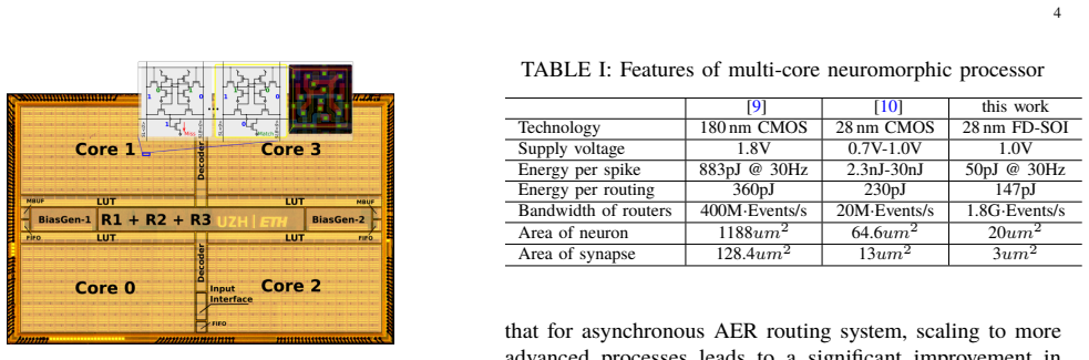
On the strength of transistor-level and Monte Carlo simulations, the paper claims that the subthreshold analog integrate-and-fire neuron, a design normally confined to 180 nm or older CMOS, can operate reliably in a 28 nm FD-SOI process. By giving current-critical and mismatch-critical transistors large channel lengths (e.g., $L_P = 100$ nm, $L_N = 200$ nm, and $500$ nm/$500$ nm for the most sensitive devices), the authors suppress leakage and random mismatch enough that a 500-run Monte Carlo simulation centered at 92.7 Hz firing rate shows a standard deviation of 5.43 Hz, a relative error of 5.86%. The same circuit reproduces tunable leak time constants, firing thresholds, refractory periods, and spike-frequency adaptation. The layout shrinks the neuron to about 20 µm² excluding capacitors, with MIM capacitors adding roughly 50 µm² for $C_M = 0.5$ pF, $C_A = 0.2$ pF, and $C_R = 0.2$ pF. The paper also reports a 10-bit PCHB-based asynchronous buffer at 1.8 G events/s with 250 µW power, and estimates a full routing system at 100 k events/s would consume about 14.7 µW, or 147 pJ per event, while CAM-based synapses, not neurons, would dominate chip area.
Load-bearing premise
The entire reliability case rests on simulation: the paper assumes the 28 nm FD-SOI process design kit's Monte Carlo and leakage models predict real silicon behavior for subthreshold currents in the picoampere range, and no fabricated chip is presented to confirm it.
Editorial extensions
If this is right
- If the simulations are right, subthreshold analog neurons no longer require large-geometry CMOS; a 20 µm² neuron (plus MIM capacitors) makes dense, biologically plausible spiking networks feasible in a commercial advanced node.
- Energy per spike of 50 pJ at 30 Hz, versus 883 pJ in the 180 nm reference and 2.3–30 nJ in a 28 nm bulk-CMOS switched-capacitor design, would put analog neuromorphic cores in range for battery-powered and closed-loop edge applications.
- The asynchronous AER router's 1.8 G events/s bandwidth would remove spike-routing bottlenecks in multi-core systems, while its power scales linearly with event rate and static power floors near 9.84 nW per buffer at low rates.
- Because a 64-fan-in, 12-bit CAM synapse block costs about 192 µm² versus 20 µm² for the neuron, the paper's scaling conclusion is that synaptic memory, not analog circuitry, dominates die area, so RRAM integration is the natural next step.
Reading between the lines
- If a fabricated 28 nm FD-SOI test chip confirms the Monte Carlo predictions, the practical barrier to analog neuromorphic scaling is not the transistor physics but the accuracy of PDK models at picoampere currents; the same sizing recipe could then be ported to other FD-SOI nodes.
- A natural testable extension is to measure firing-rate variability across many chips and temperatures and compare it to the simulated 5.86% coefficient of variation; disagreement would pinpoint which device parameters the model misrepresents.
- The reported dominance of CAM area suggests that the roadmap for neuromorphic density in advanced nodes will be set by memory technology (e.g., RRAM) rather than by analog neuron design, a shift in emphasis from circuit design to memory integration.
Signed reviews
Editorial analysis
A structured set of objections, weighed in public.
Referee Report
Summary. The paper presents a simulation-based scaling study of mixed-signal neuromorphic circuits in 28nm FD-SOI technology. It analyzes subthreshold analog neuron design by transistor sizing, asynchronous PCHB-based AER routing buffers, and CAM-based synaptic memories, reporting a neuron area of about 20um2 (excluding capacitor), an energy per spike of 50pJ at 30Hz, and a 10-bit routing buffer bandwidth of 1.8G events/s. The claims are supported by circuit simulations, including a 500-run Monte Carlo analysis of the neuron, and are compared against prior 180nm CMOS and 28nm CMOS systems.
Significance. If the results were confirmed by silicon measurements, the paper would demonstrate that mixed-signal neuromorphic circuits can indeed scale to an advanced FD-SOI node while preserving millisecond time constants and improving area and energy efficiency. The Monte Carlo analysis is a concrete step toward robustness evaluation, and the explicit comparison with a measured 28nm CMOS system provides a useful reference point. However, the central reliability claim currently rests entirely on unvalidated PDK simulations at pA current levels, with no fabricated test structures. The significance is therefore conditional on future silicon validation.
major comments (4)
- [Section II.A, Fig. 3] The claim of reliable neuron operation in 28nm FD-SOI rests on a single Monte Carlo simulation at one operating condition. A 500-run Monte Carlo at one bias point (mean firing rate 92.74Hz, standard deviation 5.43Hz) does not demonstrate robustness to temperature, supply voltage, or process-corner variation, which are especially critical for subthreshold circuits operating with pA-level currents. The paper should either report PVT corner simulations and a temperature sweep, or explicitly restrict the reliability claim to nominal conditions.
- [Table I] Table I compares simulation-based figures for 'this work' with measured values from prior fabricated systems ([9] and [10]) without flagging this asymmetry. The energy per spike, routing energy, bandwidth, and area numbers in the 'this work' column are simulation predictions, while the comparison columns are silicon measurements. The table should clearly mark which entries are simulated and which are measured, and the text should discuss the expected accuracy of the simulation estimates.
- [Section II.C] The CAM area estimate of less than 0.25um2 per cell in 28nm FD-SOI is speculative because no 28nm CAM layout or circuit simulation is presented; the 330F^2 figure from a 180nm process is simply assumed to scale. Since the paper concludes that CAMs would dominate chip area, this estimate is load-bearing for the architecture-area projection. The authors should provide a design-rule-based layout estimate or clearly qualify the conclusion as a rough projection.
- [Section II.B] The projected total routing power of 14.7uW at 100k events/s is obtained by scaling a single 10-bit buffer result to an equivalent of 600 buffers. This assumes that the buffer power scales linearly and that the 600-buffer equivalence is accurate, but no full router simulation is presented. The 147pJ/event figure should be validated with a multi-stage router simulation or a more explicit power model that includes merge, split, and memory access costs.
minor comments (5)
- [Abstract] The phrase 'deep sub-micron, mixed-signal design' is grammatically awkward; consider 'mixed-signal design in deep-submicron technologies'.
- [Fig. 1 caption] The caption contains a typo: 'Simulated channel currentID of versus VGS' should read 'Simulated channel current ID versus VGS'.
- [Section II.C] The text uses '28nm FPSOI' once; this should be '28nm FD-SOI'.
- [Section II.C] The term 'Content Addressable Memorys' should be 'Content-Addressable Memories'.
- [Fig. 3 caption] There is a spacing error in '(Std_Dev/M ean)'; it should read '(StdDev/Mean)'.
Circularity Check
No significant circularity: the paper's scaling claims are simulation-based and benchmarked against an external 28 nm CMOS system; self-citations serve as design continuity rather than load-bearing derivation.
full rationale
The paper's derivation chain is a simulation study: choose transistor sizes, simulate subthreshold currents, optimize the neuron, run Monte Carlo, report firing-rate statistics, and compare with an external 28 nm CMOS neuromorphic system in Table I. No equation in the paper fits a parameter to the claimed output and then re-presents that fit as a prediction. The prior 180 nm neuron [6] is used as a design reference and to motivate the pA-level operating currents needed for millisecond time constants, but the 28 nm results themselves come from fresh FD-SOI PDK simulations, not from [6]. The external comparison to [10] provides an independent benchmark, so the central scaling claim does not reduce to the authors' own prior work or to a self-citation chain. The absence of fabricated silicon measurements is an external-validity limitation, not a circularity: the conclusion about reliable 28 nm operation is conditional on PDK model accuracy, but no circular step is present in the paper's stated methods.
Assumptions & free parameters
free parameters (3)
- Transistor sizing for mismatch and leakage =
LP=100 nm, LN=200 nm, and 500 nm/500 nm for key transistors (e.g., MNa5 and MK4)
- MIM capacitance density =
18 fF/um2
- Neuron bias voltages and currents =
Set to obtain mean firing rate near 100 Hz (Monte Carlo result 92.74 Hz)
assumptions (2)
- domain assumption The 28 nm FD-SOI PDK models accurately represent real device leakage, mismatch, and subthreshold behavior.
- domain assumption Subthreshold operation with currents from a few pA to tens of nA remains practical in 28 nm FD-SOI with appropriate transistor sizing.
Cite this review
Pith. "Pith review of Scaling mixed-signal neuromorphic processors to 28 nm FD-SOI technologies." pith.science (2026). https://pith.science/paper/Q6LCTBZH
@misc{pith2026190807411,
  author       = {Pith},
  title        = {Pith review of: Scaling mixed-signal neuromorphic processors to 28 nm FD-SOI technologies},
  year         = {2026},
  howpublished = {\url{https://pith.science/paper/Q6LCTBZH}},
  note         = {Machine review of arXiv:1908.07411}
}
read the original abstract
As processes continue to scale aggressively, the design of deep sub-micron, mixed-signal design is becoming more and more challenging. In this paper we present an analysis of scaling multi-core mixed-signal neuromorphic processors to advanced 28 nm FD-SOI nodes. We address analog design issues which arise from the use of advanced process, including the problem of large leakage currents and device mismatch, and asynchronous digital design issues. We present the outcome of Monte Carlo Analysis and circuit simulations of neuromorphic sub threshold analog/digital neuron circuits which reproduce biologically plausible responses. We describe the AER used to implement PCHB based asynchronous QDI routing processes in multi-core neuromorphic architectures and validate their operation via circuit simulation results. Finally we describe the implementation of custom 28 nm CAM based memory resources utilized in these multi-core neuromorphic processor and discuss the possibility of increasing density by using advanced RRAM devices integrated in the 28 nm Fully-Depleted Silicon on Insulator (FD-SOI) process.
Figures


Figures from the paper (2 more)

Reference graph
Works this paper leans on
-
[9]
Neuromorphic architectures for spiking deep neural networks,
G. Indiveri, F. Corradi, and N. Qiao, “Neuromorphic architectures for spiking deep neural networks,” inElectron Devices Meeting (IEDM), 2015 IEEE International. IEEE, Dec. 2015, pp. 4.2.1–4.2.14. [Online]. Available: http://ncs.ethz.ch/pubs/pdf/Indiveri_etal15.pdf
work page 2015
-
[10]
C. Mayr, J. Partzsch, M. Noack, S. Hänzsche, S. Scholze, S. Höppner, G. Ellguth, and R. Schüffny, “A biological-realtime neuromorphic system in 28 nm cmos using low-leakage switched capacitor circuits,”IEEE transactions on biomedical circuits and systems, vol. 10, no. 1, pp. 243–254, 2016
work page 2016
-
[1]
Deep learning,
Y. LeCun, Y. Bengio, and G. Hinton, “Deep learning,”Nature, vol. 521, no. 7553, pp. 436–444, 2015
2015
-
[2]
A million spiking-neuron integrated circuit with a scalable communication network and interface,
P. A. Merolla, J. V. Arthur, R. Alvarez-Icaza, A. S. Cassidy, J. Sawada, F. Akopyan, B. L. Jackson, N. Imam, C. Guo, Y. Nakamura, B. Brezzo, I. Vo, S. K. Esser, R. Appuswamy, B. Taba, A. Amir, M. D. Flickner, W. P. Risk, R. Manohar, and D. S. Modha, “A million spiking-neuron integrated circuit with a scalable communication network and interface,” Science,...
work page 2014
-
[3]
Neurogrid: A mixed-analog-digital multichip system for large-scale neural simulations,
B. V. Benjamin, P. Gao, E. McQuinn, S. Choudhary, A. R. Chan- drasekaran, J. Bussat, R. Alvarez-Icaza, J. Arthur, P. Merolla, and K. Boahen, “Neurogrid: A mixed-analog-digital multichip system for large-scale neural simulations,”Proceedings of the IEEE, vol. 102, no. 5, pp. 699–716, 2014
work page 2014
-
[4]
S. Furber, F. Galluppi, S. Temple, and L. Plana, “The SpiNNaker project,” Proceedings of the IEEE, vol. 102, no. 5, pp. 652–665, May 2014
work page 2014
-
[5]
Neuromorphic electronic circuits for building autonomous cognitive systems,
E. Chicca, F. Stefanini, C. Bartolozzi, and G. Indiveri, “Neuromorphic electronic circuits for building autonomous cognitive systems,” Proceedings of the IEEE, vol. 102, no. 9, pp. 1367–1388, Sep 2014. [Online]. Available: http://ncs.ethz.ch/pubs/pdf/Chicca_etal14.pdf
work page 2014
-
[6]
N. Qiao, H. Mostafa, F. Corradi, M. Osswald, F. Stefanini, D. Sumislawska, and G. Indiveri, “A re-configurable on-line learning spiking neuromorphic processor comprising 256 neurons and 128k synapses,” Frontiers in Neuroscience, vol. 9, no. 141,
Show all 11 references
-
[7]
Memory and information processing in neuromorphic systems,
G. Indiveri and S.-C. Liu, “Memory and information processing in neuromorphic systems,”Proceedings of the IEEE, vol. 103, no. 8, pp. 1379–1397, 2015. [Online]. Available: http://ncs.ethz.ch/pubs/pdf/ Indiveri_Liu15.pdf
2015
-
[8]
S.-C. Liu, J. Kramer, G. Indiveri, T. Delbruck, and R. Douglas,Analog VLSI:Circuits and Principles. MIT Press, 2002. [Online]. Available: http://ncs.ethz.ch/pubs/pdf/Liu_etal02b.pdf
2002
-
[2015]
Available: http://www.frontiersin.org/neuromorphic_ engineering/10.3389/fnins.2015.00141/abstract
[Online]. Available: http://www.frontiersin.org/neuromorphic_ engineering/10.3389/fnins.2015.00141/abstract
2015
Reviewed August 14, 2026 · model on record in the stance chip above.
Discussion (0). Continue with ORCID to comment.