REVIEW 3 major objections 6 minor 10 references
A bi-directional Address-Event transceiver block for low-latency inter-chip communication in neuromorphic systems
T0 review · 3 major / 6 minor · reviewed 2026-08-14 · deepseek-v4-flash
Pith's one-line read Two neuromorphic chips can share one parallel Address-Event bus and flip its direction on a per-event basis with 5 ns latency, roughly halving I/O pins.
desk verdict A measured, useful bidirectional AER link whose main open question is the tristate turn-around handshake; worth peer review with a demand for timing analysis. read the letter →
The pith
A machine-rendered reading of the paper's core claim, the machinery that carries it, and where it could break.
The reading
What carries the argument
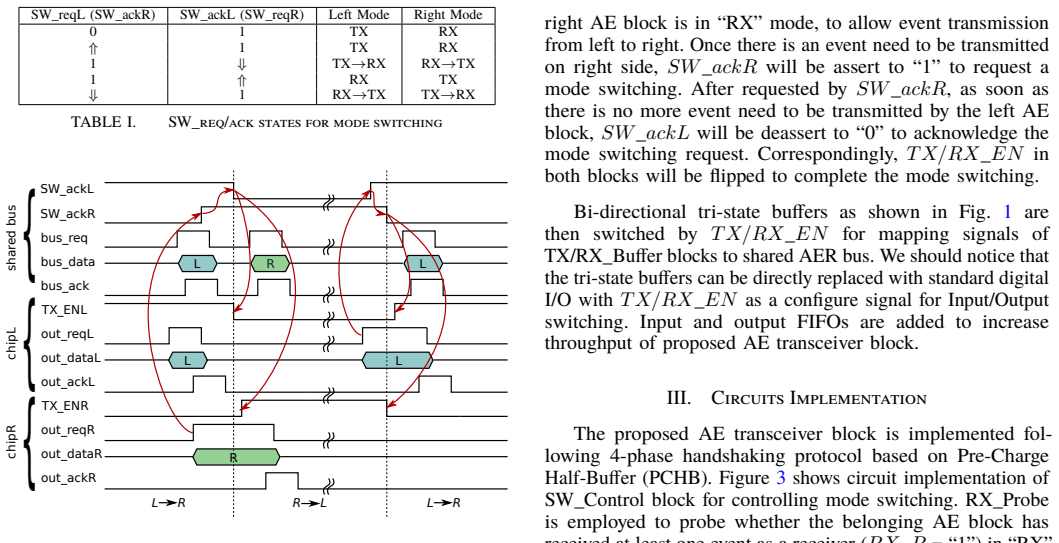
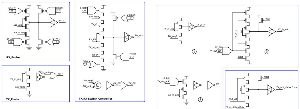
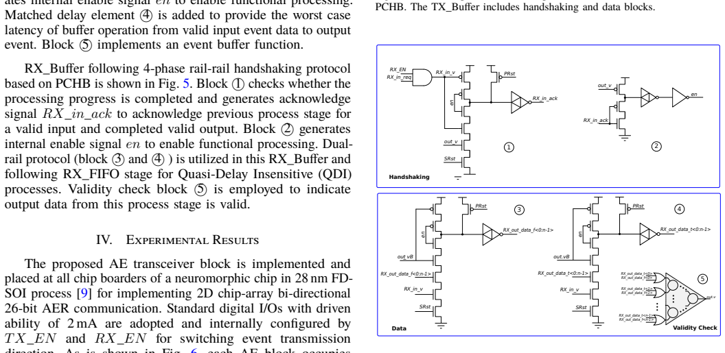
The load-bearing mechanism is the SW_Control arbitration block on each chip, together with the swapped SW_req and SW_ack wires that connect the two blocks. A block raises SW_ack when it wants to transmit and watches SW_req to see whether its partner is asking for the bus; the resulting TX_EN and RX_EN signals switch tri-state buffers, or standard digital I/Os configured as inputs or outputs, so that only one transmitter drives the shared bus at a time. RX_Probe and TX_Probe circuits guard the mode changes: a block only requests a switch from receiver to transmitter after it has actually received at least one event, and only grants a switch from transmitter to receiver when it has no event left to send. The transmit and receive buffers are implemented with pre-charge half-buffer (PCHB) four-phase handshaking, with a bundled-data path for the transmitter and a dual-rail quasi-delay-insensitive path for the receiver.
What would settle it
Take two of the fabricated transceiver chips, send back-to-back events from both sides while sweeping supply voltage and temperature, and monitor the shared data lines for contention glitches or corrupted 26-bit events; any cycle in which both transmit-enable signals are high or a bus value matches neither sender would falsify the arbitration guarantee. A formal reachability analysis of the SW_Control state machine that finds a state with transmit enabled on both blocks would do the same.
Extended reading notes
Core claim
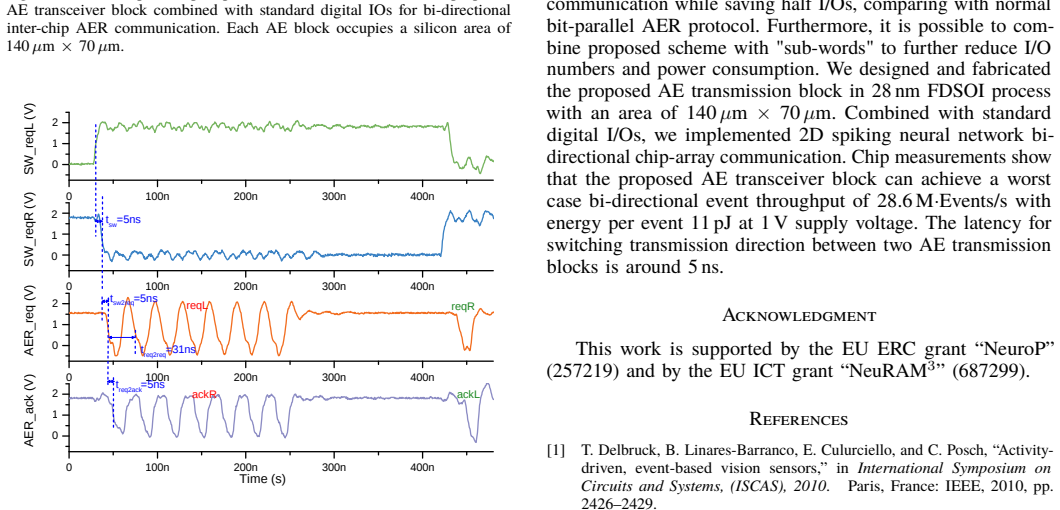
The central claim is that a fully asynchronous transceiver block makes a single shared parallel AER bus bidirectional, switching transmission direction on a single-event basis from either side. Two blocks, one on each chip, exchange swapped SW_req and SW_ack wires; each block's SW_Control uses these states to assert TX_EN or RX_EN, mapping either the transmit buffer or the receive buffer onto the shared bus. The paper reports that the scheme works in a fabricated 28 nm FDSOI neuromorphic chip: direction switching takes about 5 ns, one-direction traffic sustains 32.3M events/s, worst-case bidirectional traffic sustains 28.6M events/s, each 26-bit event costs 11 pJ at 1 V, and each block occupies 140 µm × 70 µm and saves 100 of the prototype's 180 I/O pins.
Load-bearing premise
The whole design rests on the assumption that the two sides' direction-switching negotiation can never let both transmitters drive the shared bus at the same time; the paper states the switching rules but gives no formal proof, no timing analysis, and no test of how the arbitration behaves under voltage, temperature, or manufacturing variation.
Editorial extensions
If this is right
- A two-chip link needs one parallel bus instead of two, so a tiled neuromorphic system can roughly halve its inter-chip AER pin count; the prototype is reported to save 100 of 180 I/O pins.
- Because direction can be switched per event, mixed traffic from both sides can alternate on the same wires without waiting for a long bus-turnaround phase, keeping spike latency near the single-direction value.
- The fully asynchronous design needs no clock generation or synchronization circuitry, unlike bit-serial LVDS AER links, so it fits naturally into asynchronous neuromorphic processors.
- The measured 28.6M events/s worst-case bidirectional throughput and 11 pJ per event at 1 V give a concrete budget for building 2D chip arrays with north/south/east/west links.
- The paper states the scheme can be combined with sub-word transmission to reduce I/O pins and power further, beyond the demonstrated halving.
Reading between the lines
- A likely consequence not tested in the paper is that the per-event arbitration makes effective throughput nearly independent of traffic direction until the bus approaches saturation; a simple experiment with Poisson arrivals from both sides would show whether the worst-case 28.6M events/s figure is approached gracefully.
- The same SW_Control arbitration is not specific to AER: any asynchronous packetized bus with a request/acknowledge protocol could use this style of per-transaction direction switching, so the block is a candidate building block for asynchronous network-on-chip links.
- Because the TX buffer relies on a matched-delay element for bundled-data timing, the design's margins may shrink at low supply voltages or extreme temperatures; stress-testing the 5 ns switch latency across voltage and temperature corners would reveal how far the claim generalizes.
- The paper excludes digital I/O power from the 11 pJ per-event figure, so a full system-level energy comparison against two unidirectional buses would need to include pad driver and pin capacitance costs.
Signed reviews
Editorial analysis
A structured set of objections, weighed in public.
Referee Report
Summary. The manuscript describes a fully asynchronous bidirectional Address-Event (AE) transceiver block for inter-chip neuromorphic communication. The block uses a SW_Control handshake between two linked chips to arbitrate the direction of a single shared parallel AER bus, with TX_EN/RX_EN signals configuring standard tristate digital I/Os. The authors report a 28 nm FDSOI implementation occupying 140 µm × 70 µm that achieves a measured direction-switch latency of 5 ns, a single-direction throughput of 32.3M events/s, a bidirectional worst-case throughput of 28.6M events/s, and 11 pJ per 26-bit event at 1 V, with the caveat that the energy figure excludes digital I/O power. The central claims are that the block halves I/O pin count relative to two unidirectional buses while preserving low-latency event-driven operation.
Significance. The contribution is potentially useful: it provides a concrete, silicon-validated building block for low-latency bidirectional AER links, and the measured waveforms and key figures support the feasibility of the approach. The 5 ns direction-switch latency and 28.6M events/s bidirectional throughput are competitive with existing asynchronous AER links, and the compatibility with standard digital I/Os is a practical advantage. The paper's strengths include a fabricated 28 nm FDSOI test chip, explicit measurement of the switching transient, and a compact layout. However, the load-bearing mutual-exclusion property of the bus-direction handshake is not established by timing analysis, formal reasoning, or contention measurement, so the reliability claim rests on an unverified assumption. If that gap is closed, the design would be a solid contribution to practical neuromorphic inter-chip communication.
major comments (3)
- [Section III, Fig. 3 and Table I] The SW_Control handshake guarantees only logical mode agreement (one side in TX, the other in RX); it does not guarantee that the two tristate driver banks are never simultaneously enabled during the direction transition. The text gives no disable-before-enable timing constraint, no min/max delay for TX_EN falling versus TX_EN rising, and no process-corner, Monte Carlo, or stress-test analysis. If the delay from SW_ackL falling to TX_ENL falling plus the I/O disable time is shorter than the corresponding path through SW_reqR to TX_ENR rising plus the I/O enable time, both drivers are active for the skew window. This would cause bus contention, corrupt events, and potentially damage the I/O pads. The measured 5 ns switching latency in Section IV does not bound the worst-case overlap because it is a single nominal measurement. The authors should add a timing analysis of the turnaround path, or a direct contention/current measurement, or an explicit completion-detection mechanism on the tristate-disable path.
- [Section IV, energy measurement] The paper reports 11 pJ per 26-bit event at 1 V, but explicitly states that this excludes power consumption from the digital I/Os, even though the block is combined with standard digital I/Os and the I/O buffers are part of the measured link. Since the tristate I/O drivers often dominate bus power, this figure is not the full per-event delivery energy of the link. The authors should report the complete link energy including the digital I/Os, or state clearly that 11 pJ covers only the transceiver core and provide the I/O energy separately.
- [Section IV, Figs. 7 and 8] The experimental section reports single-point numbers without error bars, sample size, supply-voltage/temperature conditions, or a description of how many chips and links were measured. The throughput values labeled 'worst-case' also need the exact traffic pattern and FIFO depth to be specified; the waveforms in Figs. 7 and 8 appear to come from a single run. This matters because the 5 ns direction-switch latency and the 28.6M events/s bidirectional throughput are the paper's headline claims, and the current presentation does not allow the reader to assess their variability or the conditions under which they hold.
minor comments (6)
- [Section I] The Introduction contains unresolved placeholder references '[?]' in two places, as well as '[?], [7]'; these citations should be filled in before submission.
- [Section II] The text says 'its lined AE block' where it should say 'its linked AE block'.
- [Section IV] The phrase 'continuously events communing from left' should be corrected to 'continuously coming from left'.
- [Figure 2] The labels 'L R L RR L' at the bottom of Figure 2 are cryptic and should be expanded in the caption or replaced with a clearer timing diagram explaining the bus-ownership sequence.
- [Figure 8] The waveform labels in Figure 8 are duplicated (e.g., 'ackL' appears multiple times), making it difficult to identify which node each trace corresponds to; the traces should be re-labeled clearly.
- [Section IV] The paper should define exactly how the 'worst-case bidirectional throughput' was measured, including whether events are alternated on a single-event basis or sent in bursts, since this determines whether the 28.6M events/s figure is truly a worst-case value.
Circularity Check
No significant circularity: the paper reports direct chip measurements of a hardware transceiver, with no fitted parameters or self-cited result serving as the basis for its central claims.
full rationale
The paper's central claims are experimental results: 5 ns direction-switch latency, 32.3M events/s one-direction throughput, 28.6M events/s bidirectional throughput, and 11 pJ/event energy at 1 V, all measured on a fabricated 28 nm FDSOI chip (Section IV, Figs. 6-8, Table II). These are direct measurements, not derivations, so there is no fitted-input-called-prediction pattern and no equation-level reduction of outputs to inputs. The SW_Control mode-switching protocol in Sections II-III is a circuit design description and a proposed handshake condition; it is not presented as a theorem derived from a fitted model, and the paper does not claim to predict the measured numbers from the protocol. Self-citations by the authors (e.g., refs. [3], [4], [9]) are used for background on neuromorphic systems and the 28 nm FDSOI test chip, but they are not load-bearing for the reported throughput, latency, or energy figures. A possible concern is the lack of a formal timing bound proving that the tristate drivers are never simultaneously enabled during direction switching; however, that is a correctness/reliability risk about arbitration, not circularity. No circular step meeting the quoted-evidence standard was found.
Assumptions & free parameters
assumptions (2)
- domain assumption The 4-phase PCHB handshaking and the SW_Control state machine correctly arbitrate bus direction without contention or deadlock.
- domain assumption Standard digital I/O buffers configured as tri-state drivers behave as assumed and switch direction within the timing constraints set by TX_EN and RX_EN.
Cite this review
Pith. "Pith review of A bi-directional Address-Event transceiver block for low-latency inter-chip communication in neuromorphic systems." pith.science (2026). https://pith.science/paper/QIUPQR2O
@misc{pith2026190807413,
  author       = {Pith},
  title        = {Pith review of: A bi-directional Address-Event transceiver block for low-latency inter-chip communication in neuromorphic systems},
  year         = {2026},
  howpublished = {\url{https://pith.science/paper/QIUPQR2O}},
  note         = {Machine review of arXiv:1908.07413}
}
read the original abstract
Neuromorphic systems typically use the Address-Event Representation (AER) to transmit signals among nodes, cores, and chips. Communication of Address-Events (AEs) between neuromorphic cores/chips typically requires two parallel digital signal buses for Input/Output (I/O) operations. This requirement can become very expensive for large-scale systems in terms of both dedicated I/O pins and power consumption. In this paper we present a compact fully asynchronous event-driven transmitter/receiver block that is both power efficient and I/O efficient. This block implements high-throughput low-latency bi-directional communication through a parallel AER bus. We show that by placing the proposed AE transceiver block in two separate chips and linking them by a single AER bus, we can drive the communication and switch the transmission direction of the shared bus on a single event basis, from either side with low-latency. We present experimental results that validate the circuits proposed and demonstrate reliable bi-directional event transmission with high-throughput. The proposed AE block, integrated in a neuromorphic chip fabricated using a 28 nm FDSOI process, occupies a silicon die area of 140 {\mu}m x 70 {\mu}m. The experimental measurements show that the event-driven AE block combined with standard digital I/Os has a direction switch latency of 5 ns and can achieve a worst-case bi-directional event transmission throughput of 28.6M Events/second while consuming 11 pJ per event (26-bit) delivery.
Figures

Figures from the paper (4 more)


Reference graph
Works this paper leans on
-
[1]
T. Delbruck, B. Linares-Barranco, E. Culurciello, and C. Posch, ``Activity-driven, event-based vision sensors,'' in International Symposium on Circuits and Systems, ( ISCAS ), 2010 . 1em plus 0.5em minus 0.4em Paris, France: IEEE, 2010, pp. 2426--2429
work page 2010
-
[2]
S.-C. Liu, A. van Schaik, B. Minch, T. Delbruck et al., ``Asynchronous binaural spatial audition sensor with 2x64 4 channel output,'' Biomedical Circuits and Systems, IEEE Transactions on , vol. 8, no. 4, pp. 453--464, 2014
work page 2014
-
[3]
N. Qiao, H. Mostafa, F. Corradi, M. Osswald, F. Stefanini, D. Sumislawska, and G. Indiveri, ``A re-configurable on-line learning spiking neuromorphic processor comprising 256 neurons and 128k synapses,'' Frontiers in Neuroscience, vol. 9, no. 141, 2015. [Online]. Available: http://www.frontiersin.org/neuromorphic_engineering/10.3389/fnins.2015.00141/abstract
arXiv 2015
-
[4]
S. Moradi, N. Qiao, F. Stefanini, and G. Indiveri, ``A scalable multi-core architecture with heterogeneous memory structures for dynamic neuromorphic asynchronous processors (dynaps),'' arXiv preprint arXiv:1708.04198, 2017
work page Pith review arXiv 2017
-
[5]
G. Indiveri, F. Corradi, and N. Qiao, ``Neuromorphic architectures for spiking deep neural networks,'' in Electron Devices Meeting (IEDM) , 2015 IEEE International . 1em plus 0.5em minus 0.4em IEEE, Dec. 2015, pp. 4.2.1--4.2.14. [Online]. Available: http://ncs.ethz.ch/pubs/pdf/Indiveri_etal15.pdf
work page 2015
-
[6]
P. A. Merolla, J. V. Arthur, R. Alvarez-Icaza, A. S. Cassidy, J. Sawada, F. Akopyan, B. L. Jackson, N. Imam, C. Guo, Y. Nakamura, B. Brezzo, I. Vo, S. K. Esser, R. Appuswamy, B. Taba, A. Amir, M. D. Flickner, W. P. Risk, R. Manohar, and D. S. Modha, ``A million spiking-neuron integrated circuit with a scalable communication network and interface,'' Scienc...
work page 2014
-
[7]
C. Brandli, R. Berner, M. Yang, S.-C. Liu, and T. Delbruck, ``A 240 180 130 d B 3 s latency global shutter spatiotemporal vision sensor,'' IEEE Journal of Solid-State Circuits , vol. 49, no. 10, pp. 2333--2341, 2014
work page 2014
-
[8]
C. Zamarre \ n o-Ramos, R. Kulkarni, J. Silva-Mart \' nez, T. Serrano-Gotarredona, and B. Linares-Barranco, ``A 1.5 ns off/on switching-time voltage-mode lvds driver/receiver pair for asynchronous aer bit-serial chip grid links with up to 40 times event-rate dependent power savings,'' IEEE transactions on biomedical circuits and systems, vol. 7, no. 5, pp...
work page 2013
Show all 10 references
-
[9]
Qiao and G
N. Qiao and G. Indiveri, ``Scaling mixed-signal neuromorphic processors to 28 nm fd-soi technologies,'' in Biomedical Circuits and Systems Conference (BioCAS), 2016 IEEE. 1em plus 0.5em minus 0.4em IEEE, 2016, pp. 552--555
2016
-
[10]
C Î) :@@wm; c[&>Sc1h df e;r 9LF=̎ 6] 'i@6l6! Sǘ!tNۺ b4KT ǵXK lT/ ^ShЕ? ¡)ղlf* ? f bU' djا5he] lM柮ٳe h& B s ƛZ!A]th !8 u B440 B i !s8CTan/I BAM[B bc^gX ,XFS4
11em plus .33em minus .07em 4000 4000 100 4000 4000 500 `\.=1000 = #1 \@IEEEnotcompsoconly \@IEEEcompsoconly #1 * [1] 0pt [0pt][0pt] #1 * \| ** #1 \@IEEEauthorblockNstyle \@IEEEcompsocnotconfonly \@IEEEcompsocconfonly \@IEEEauthorblockAstyle \@IEEEcompsocnotconfonly \@IEEEcomp...
1956
Reviewed August 14, 2026 · model on record in the stance chip above.
Discussion (0). Continue with ORCID to comment.