Atomic-Scale Characterization of Oxide Interfaces and Superlattices Using Scanning Transmission Electron Microscopy
Pith reviewed 2026-07-01 01:27 UTC · model grok-4.3
The pith
Scanning transmission electron microscopy provides unmatched atomic-scale insight into oxide interfaces and superlattices.
A machine-rendered reading of the paper's core claim, the machinery that carries it, and where it could break.
Core claim
STEM is a cornerstone of our understanding of oxide interfaces and superlattices. No other technique provides the same level of insight into structure, chemistry, composition, and dynamics across as wide a variety of material systems. STEM imaging and diffraction, coupled with electron energy loss (EELS) and energy-dispersive X-ray (EDS) spectroscopies, offer unparalleled, high-resolution analysis of structure-property relationships.
What carries the argument
Scanning transmission electron microscopy (STEM) imaging, diffraction, EELS, and EDS for atomic-scale analysis of structure, chemistry, composition, and dynamics.
Load-bearing premise
The selected investigations into interfacial conductivity, charge screening, and iron oxides accurately represent the most important phenomena without selection bias.
What would settle it
Demonstration of another technique achieving comparable atomic-scale resolution, chemical mapping, and dynamic insight across oxide superlattices would challenge the uniqueness of STEM.
Figures
read the original abstract
Scanning transmission electron microscopy (STEM) is a cornerstone of our understanding of oxide interfaces and superlattices. No other technique provides the same level of insight into structure, chemistry, composition, and dynamics across as wide a variety of material systems. STEM imaging and diffraction, coupled with electron energy loss (EELS) and energy-dispersive X-ray (EDS) spectroscopies, offer unparalleled, high-resolution analysis of structure--property relationships. In this chapter we highlight investigations into key phenomena, including interfacial conductivity in oxide superlattices, charge screening effects in magnetoelectric heterostructures, interface engineering in iron oxides, and the complex physics governing atomic-scale chemical mapping. We also discuss emerging plasma preparation techniques and artificial intelligence-guided approaches to both ex situ and in situ microscopy. These studies illustrate how unique insights from STEM characterization can be integrated with other techniques and theory calculations to develop more predictive models for the behavior of functional oxides.
Editorial analysis
A structured set of objections, weighed in public.
Referee Report
Summary. This review chapter positions scanning transmission electron microscopy (STEM), combined with EELS and EDS spectroscopies, as a cornerstone technique for atomic-scale characterization of oxide interfaces and superlattices. It claims that no other method matches STEM's insight into structure, chemistry, composition, and dynamics across material systems. The chapter summarizes prior investigations into interfacial conductivity in oxide superlattices, charge screening in magnetoelectric heterostructures, interface engineering in iron oxides, and atomic-scale chemical mapping, while also covering emerging plasma preparation methods and AI-guided ex situ/in situ approaches. Emphasis is placed on integrating STEM results with other techniques and theory to build predictive models for functional oxides.
Significance. As a review without new derivations or experimental claims, the manuscript's significance rests on the balance and utility of its synthesis of established STEM capabilities. The positioning statement regarding STEM's unique level of insight is a standard framing in the field and is illustrated via the selected example studies. Credit is due for explicitly noting integration with theory calculations and other experimental methods. The selection of phenomena (conductivity, charge screening, iron oxides) appears representative of active research areas rather than introducing evident selection bias, consistent with the stress-test concern not landing as a load-bearing issue.
minor comments (1)
- The abstract states the central positioning claim without qualification; if the full chapter includes a dedicated limitations or comparison section, cross-referencing it would strengthen the claim.
Simulated Author's Rebuttal
We thank the referee for their constructive review and for recommending acceptance of the manuscript. The report contains no major comments requiring a point-by-point response.
Circularity Check
No significant circularity; review chapter with no derivations
full rationale
The paper is a review summarizing established STEM techniques and citing example studies on oxide interfaces. It contains no equations, predictions, fitted parameters, or derivation chains. The central claim about STEM's unique insight level is a positioning statement supported by external citations rather than an internal reduction to self-defined inputs. No load-bearing steps reduce to self-citation chains or ansatzes. This matches the default expectation for non-derivational review content.
Axiom & Free-Parameter Ledger
Reference graph
Works this paper leans on
-
[1]
The correction of electron lens aberrations.Ultramicroscopy156,A1–A64
Hawkes, P. The correction of electron lens aberrations.Ultramicroscopy156,A1–A64. doi:10. 1016/j.ultramic.2015.03.007(2015)
2015
-
[2]
L.et al.An electron microscope for the aberration-corrected era.Ultramicroscopy 108,179–95
Krivanek, O. L.et al.An electron microscope for the aberration-corrected era.Ultramicroscopy 108,179–95. doi:10.1016/j.ultramic.2007.07.010(Feb. 2008)
-
[3]
Muller, D. A.et al.Atomic-scale chemical imaging of composition and bonding by aberration- corrected microscopy.Science319,1073–6. doi:10.1126/science.1148820(Feb. 2008)
-
[4]
Bosman, M.et al.Two-Dimensional Mapping of Chemical Information at Atomic Resolution.Phys. Rev. Lett.99,086102. doi:10.1103/PhysRevLett.99.086102(Aug. 2007)
-
[5]
Kimoto, K.et al.Element-selective imaging of atomic columns in a crystal using STEM and EELS. Nature450,702–704. doi:10.1038/nature06352(2007)
-
[6]
Varela, M.et al.Spectroscopic Imaging of Single Atoms Within a Bulk Solid.Phys. Rev. Lett.92, 095502. doi:10.1103/PhysRevLett.92.095502(Mar. 2004)
-
[7]
Batson, P. E., Dellby, N. & Krivanek, O. L. Sub-ångstrom resolution using aberration corrected electron optics.Nature418,617–20. doi:10.1038/nature00972(Aug. 2002)
-
[8]
Batson, P. E. Simultaneous STEM imaging and electron energy-loss spectroscopy with atomic- column sensitivity.Nature366,727–728. doi:10.1038/366727a0(Dec. 1993)
-
[9]
Duscher, G., Browning, N. D. & Pennycook, S. J. Atomic Column Resolved Electron Energy-Loss Spectroscopy.Phys. status solidi166,327–342. doi: 10.1002/(SICI)1521- 396X(199803)166: 1<327::AID-PSSA327>3.0.CO;2-R(Mar. 1998)
-
[10]
Browning, N. D., Chisholm, M. F. & Pennycook, S. J. Atomic-resolution chemical analysis using a scanning transmission electron microscope.Nature366,143–146. doi:10.1038/366143a0 (Nov. 1993)
-
[11]
Muller, D. A., Tzou, Y., Raj, R. & Silcox, J. Mapping sp2 and sp3 states of carbon at sub-nanometre spatial resolution.Nature366,725–727. doi:10.1038/366725a0(Dec. 1993)
-
[12]
Y.et al.Emergent phenomena at oxide interfaces.Nat
Hwang, H. Y.et al.Emergent phenomena at oxide interfaces.Nat. Mater.11,103–113. doi: 10. 1038/nmat3223(Jan. 2012)
2012
-
[13]
& Ramesh, R
Martin, L., Chu, Y.-H. & Ramesh, R. Advances in the growth and characterization of magnetic, ferroelectric, and multiferroic oxide thin films.Mater. Sci. Eng. R Reports68,89–133. doi: 10. 1016/j.mser.2010.03.001(May 2010)
2010
-
[14]
Ramesh, R. & Spaldin, N. a. Multiferroics: progress and prospects in thin films.Nat. Mater.6, 21–9. doi:10.1038/nmat1805(Jan. 2007)
-
[15]
Chambers, S. A. Epitaxial growth and properties of doped transition metal and complex oxide films.Adv. Mater.22,219–48. doi:10.1002/adma.200901867(Jan. 2010)
-
[16]
Chambers, S. A. Epitaxial growth and properties of thin film oxides.Surf. Sci. Rep.39,105–180. doi:10.1016/S0167-5729(00)00005-4(Aug. 2000)
-
[17]
Egerton, R., Li, P. & Malac, M. Radiation damage in the TEM and SEM.Micron35,399–409. doi:10.1016/j.micron.2004.02.003(Aug. 2004). 26
-
[18]
& Kotani, A.Core Level Spectroscopy of Solids(CRC Press, 2008)
De Groot, F. & Kotani, A.Core Level Spectroscopy of Solids(CRC Press, 2008)
2008
-
[19]
doi:10.1093/jmicro/dfu011 (June 2014)
Ootsuki, S.et al.Impact of Local Strain on Ti L2,3 Electron Energy-Loss Near-Edge Structures of BaTiO3: A First-Principles Multiplet Study.Microscopy63,249–254. doi:10.1093/jmicro/dfu011 (June 2014)
-
[20]
Lopata, K. & Govind, N. Near and above ionization electronic excitations with non-hermitian real-time time-dependent density functional theory.J. Chem. Theory Comput.9,4939–4946. doi:10.1021/ct400569s(2013)
-
[21]
Ootsuki, S.et al.Ab-Initio Multiplet Calculation of Oxygen Vacancy Effect on TiL2,3 Electron EnergyLossNearEdgeStructuresofBaTiO 3.Appl. Phys. Lett.99,233109.doi: 10.1063/1.3663543 (Dec. 2011)
-
[22]
Simulation in Elemental Mapping Using Aberration-Corrected Electron Microscopy
Allen, L. Simulation in Elemental Mapping Using Aberration-Corrected Electron Microscopy. Ultramicroscopy178,110–120. doi:10.1016/j.ultramic.2017.03.001(July 2017)
-
[23]
Allen, L., D’Alfonso, A. & Findlay, S. Modelling the inelastic scattering of fast electrons. Ultramicroscopy151,11–22. doi:10.1016/j.ultramic.2014.10.011(Apr. 2015)
-
[24]
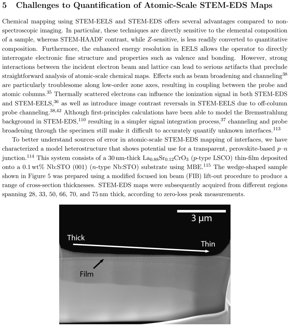
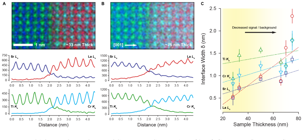
Kirkland, E. J.Advanced Computing in Electron Microscopydoi: 10.1007/978-1-4419-6533-2 (Springer US, Boston, MA, 2010)
-
[25]
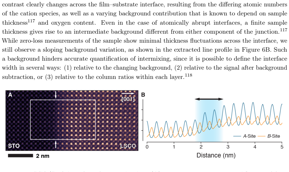
Cowley, J. M. & Moodie, A. F. The scattering of electrons by atoms and crystals. I. A new theoretical approach.Acta Crystallogr.10,609–619. doi:10.1107/S0365110X57002194(Oct. 1957)
-
[26]
Gázquez, J.et al.Applications of STEM-EELS to Complex Oxides.Mater. Sci. Semicond. Process. 65,49–63. doi:10.1016/j.mssp.2016.06.005(2017)
-
[27]
& Ramasse, Q
MacLaren, I. & Ramasse, Q. M. Aberration-corrected scanning transmission electron microscopy for atomic-resolution studies of functional oxides.Int. Mater. Rev.59,115–131. doi: 10.1179/ 1743280413Y.0000000026(Apr. 2014)
2014
-
[28]
Varela, M.et al.Materials characterization in the aberration-corrected scanning transmission electron microscope.Annu. Rev. Mater. Res.35,539–569. doi: 10.1146/annurev.matsci.35. 102103.090513(Aug. 2005)
-
[29]
Chambers, S.et al.Instability, intermixing and electronic structure at the epitaxial LaAlO3/SrTiO3(001) heterojunction.Surf. Sci. Rep.65,317–352. doi:10.1016/j.surfrep.2010.09.001(Oct. 2010)
-
[30]
Nakagawa, N., Hwang, H. Y. & Muller, D. A. Why some interfaces cannot be sharp.Nat. Mater. 5,204–209. doi:10.1038/nmat1569(Mar. 2006)
-
[31]
Cantoni, C.et al.Electron Transfer and Ionic Displacements at the Origin of the 2D Electron Gas at the LAO/STO Interface: Direct Measurements with Atomic-Column Spatial Resolution.Adv. Mater.24,3952–3957. doi:10.1002/adma.201200667(Aug. 2012)
-
[32]
Shah, A. B.et al.Probing Interfacial Electronic Structures in Atomic Layer LaMnO3 and SrTiO3 Superlattices.Adv. Mater.22,1156–1160. doi:10.1002/adma.200904198(Feb. 2010)
-
[33]
Shah, A. B.et al.Presence and spatial distribution of interfacial electronic states in LaMnO3 - SrMnO3 superlattices.Phys. Rev. B82,115112. doi: 10.1103/PhysRevB.82.115112 (Sept. 2010). 27
-
[34]
Kothleitner, G.et al.Quantitative Elemental Mapping at Atomic Resolution Using X-Ray Spectroscopy.Phys. Rev. Lett.112,085501. doi:10.1103/PhysRevLett.112.085501(2014)
-
[35]
Lugg, N., Kothleitner, G., Shibata, N. & Ikuhara, Y. On the quantitativeness of EDS STEM. Ultramicroscopy151,150–159. doi:10.1016/j.ultramic.2014.11.029(2014)
-
[36]
D.et al.Contribution of thermally scattered electrons to atomic resolution elemental maps.Phys
Forbes, B. D.et al.Contribution of thermally scattered electrons to atomic resolution elemental maps.Phys. Rev. B86,024108. doi:10.1103/PhysRevB.86.024108(2012)
-
[37]
D’Alfonso, A. J., Freitag, B., Klenov, D. & Allen, L. J. Atomic-resolution chemical mapping using energy-dispersive x-ray spectroscopy.Phys. Rev. B81,100101. doi: 10.1103/PhysRevB.81.100101 (Mar. 2010)
-
[38]
P.et al.Interpreting atomic-resolution spectroscopic images.Phys
Oxley, M. P.et al.Interpreting atomic-resolution spectroscopic images.Phys. Rev. B76,064303. doi:10.1103/PhysRevB.76.064303(Aug. 2007)
-
[40]
Gulec, A., Phillips, P. J. & Klie, R. F. Position-sensitive change in the transition metal L-edge fine structures.Appl. Phys. Lett.107,143111. doi:10.1063/1.4932637(2015)
-
[41]
Xin, H. L., Dwyer, C. & Muller, D. A. Is there a Stobbs factor in atomic-resolution STEM-EELS mapping?Ultramicroscopy139,38–46. doi:10.1016/j.ultramic.2014.01.006(Apr. 2014)
-
[43]
Dwyer, C., Findlay, S. D. & Allen, L. J. Multiple elastic scattering of core-loss electrons in atomic resolution imaging.Phys. Rev. B77,184107. doi:10.1103/PhysRevB.77.184107(May 2008)
-
[44]
R.et al.Towards Data-Driven Next-Generation Transmission Electron Microscopy
Spurgeon, S. R.et al.Towards Data-Driven Next-Generation Transmission Electron Microscopy. Nat. Mater.20,274–279. doi:10.1038/s41563-020-00833-z(2021)
-
[45]
Learn.doi:10.1063/5.0267699(2025)
Guinan, G.et al.Mind the Gap: Bridging the Divide Between AI Aspirations and the Reality of Autonomous Microscopy.APL Mach. Learn.doi:10.1063/5.0267699(2025)
-
[46]
Akers, S.et al.Rapid and Flexible Segmentation of Electron Microscopy Data Using Few-Shot Machine Learning.npj Comput. Mater.7,187. doi:10.1038/s41524-021-00652-z(2021)
-
[47]
V.et al.Machine Learning in Scanning Transmission Electron Microscopy.Nat
Kalinin, S. V.et al.Machine Learning in Scanning Transmission Electron Microscopy.Nat. Rev. Methods Primers2,11. doi:10.1038/s43586-022-00095-w(2022)
-
[48]
Ede, J. M. Deep Learning in Electron Microscopy.Mach. Learn.: Sci. Technol.2,011004. doi:10. 1088/2632-2153/abd614(2021)
2021
-
[49]
Nelson, C. T.et al.Deep Learning Ferroelectric Polarization Distributions from STEM Data via With and Without Atom Finding.npj Comput. Mater.7,149. doi: 10.1038/s41524-021-00613-6 (2021)
-
[50]
Kalinin, S. V., Ghosh, A., Vasudevan, R. K. & Ziatdinov, M. From Atomically Resolved Imaging to Generative and Causal Models.Nat. Phys.18,1152–1160. doi:10.1038/s41567-022-01666-0 (2022). 28
-
[51]
Mater.6,
Ziatdinov, M.et al.Causal Analysis of Competing Atomistic Mechanisms in Ferroelectric Materials from High-Resolution Scanning Transmission Electron Microscopy Data.npj Comput. Mater.6,
-
[52]
doi:10.1038/s41524-020-00396-2(2020)
-
[53]
Ter-Petrosyan, A.et al.Revealing the Evolution of Order in Materials Microstructures Using Multi-Modal Computer Vision.npj Comput. Mater.11,1. doi: 10.1038/s41524-025-01831-y (2025)
-
[54]
R.et al.Forecasting of In Situ Electron Energy Loss Spectroscopy.npj Comput
Lewis, N. R.et al.Forecasting of In Situ Electron Energy Loss Spectroscopy.npj Comput. Mater. 8,252. doi:10.1038/s41524-022-00940-2(2022)
-
[55]
Olszta, M.et al.An Automated Scanning Transmission Electron Microscope Guided by Sparse Data Analytics.Microsc. Microanal.28,1611–1621. doi:10.1017/S1431927622012065(2022)
-
[56]
Kalinin, S. V.et al.Automated and Autonomous Experiments in Electron and Scanning Probe Microscopy.ACS Nano15,12604–12627. doi:10.1021/acsnano.1c02104(2021)
-
[57]
Kalinin, S. V.et al.Machine Learning for Automated Experimentation in Scanning Transmission Electron Microscopy.npj Comput. Mater.9,227. doi:10.1038/s41524-023-01142-0(2023)
-
[58]
Guinan, G.et al.Revealing the Hidden Third Dimension of Point Defects in Two-Dimensional MXenes.Nat. Commun.17,3473. doi:10.1038/s41467-026-71670-y(2026)
-
[59]
M., Torsi, R., Robinson, J., Kalinin, S
Roccapriore, K. M., Torsi, R., Robinson, J., Kalinin, S. & Ziatdinov, M. Dynamic STEM-EELS for Single-Atom and Defect Measurement During Electron Beam Transformations.Sci. Adv.10, eadn5899. doi:10.1126/sciadv.adn5899(2024)
-
[60]
Mannhart, J. & Schlom, D. G. Oxide Interfaces–An Opportunity for Electronics.Science327, 1607–1611. doi:10.1126/science.1181862(Mar. 2010)
-
[61]
G.et al.Strain Tuning of Ferroelectric Thin Films.Annu
Schlom, D. G.et al.Strain Tuning of Ferroelectric Thin Films.Annu. Rev. Mater. Res.37,589–626. doi:10.1146/annurev.matsci.37.061206.113016(Aug. 2007)
work page doi:10.1146/annurev.matsci.37.061206.113016(aug 2007
-
[62]
Chen, S.et al.LaAlO 3/SrTiO3 Heterointerface: 20 Years and Beyond.Adv. Electron. Mater.10, 2300730. doi:10.1002/aelm.202300730(2024)
-
[63]
Ohtomo, A. & Hwang, H. Y. A high-mobility electron gas at the LaAlO3/SrTiO3 heterointerface. Nature427,423–426. doi:10.1038/nature02308(Jan. 2004)
-
[64]
Qiao, L.et al.Epitaxial Growth, Structure, and Intermixing at the LaAlO3/SrTiO3 Interface as the Film Stoichiometry is Varied.Phys. Rev. B83,085408. doi: 10.1103/PhysRevB.83.085408 (Feb. 2011)
-
[65]
Willmott, P.et al.Structural Basis for the Conducting Interface between LaAlO3 and SrTiO3. Phys. Rev. Lett.99,155502. doi:10.1103/PhysRevLett.99.155502(Oct. 2007)
-
[66]
B.et al.Interface-Induced Polarization in SrTiO3–LaCrO3 Superlattices.Adv
Comes, R. B.et al.Interface-Induced Polarization in SrTiO3–LaCrO3 Superlattices.Adv. Mater. Interfaces3,1500779. doi:10.1002/admi.201500779(May 2016)
-
[67]
Chambers, S. A.et al.Band Alignment, Built-In Potential, and the Absence of Conductivity at the LaCrO3 / SrTiO3 (001) Heterojunction.Phys. Rev. Lett.107,206802. doi: 10.1103/PhysRevLett. 107.206802(Nov. 2011)
-
[68]
B.et al.Probing the Origin of Interfacial Carriers in SrTiO3–LaCrO3 Superlattices
Comes, R. B.et al.Probing the Origin of Interfacial Carriers in SrTiO3–LaCrO3 Superlattices. Chem. Mater.29,1147–1155. doi:10.1021/acs.chemmater.6b04329(Feb. 2017). 29
-
[69]
Varela, M.et al.Atomic-resolution imaging of oxidation states in manganites.Phys. Rev. B79, 085117. doi:10.1103/PhysRevB.79.085117(Feb. 2009)
-
[70]
Colby, R.et al.Cation intermixing and electronic deviations at the insulating LaCrO3/SrTiO3(001) interface.Phys. Rev. B88,155325. doi:10.1103/PhysRevB.88.155325(Oct. 2013)
-
[71]
Kaspar, T. C.et al.Built-In Potential in Fe2O3–Cr2O3 Superlattices for Improved Photoexcited Carrier Separation.Adv. Mater.28,1616–1622. doi:10.1002/adma.201504545(Feb. 2016)
-
[72]
Arévalo-López, Á. M. & Alario-Franco, M. Á. Reliable Method for Determining the Oxidation State in Chromium Oxides.Inorg. Chem.48,11843–11846. doi:10.1021/ic901887y(Dec. 2009)
-
[73]
Vaz, C. A. F., Walker, F. J., Ahn, C. H. & Ismail-Beigi, S. Intrinsic interfacial phenomena in manganite heterostructures.J. Phys. Condens. Matter27,123001. doi: 10.1088/0953-8984/27/ 12/123001(2015)
-
[74]
Wang, Y., Hu, J., Lin, Y. & Nan, C.-W. Multiferroic magnetoelectric composite nanostructures. NPG Asia Mater.2,61–68. doi:10.1038/asiamat.2010.32(2010)
-
[75]
Wu, T.et al.Observation of magnetoelectric effect in epitaxial ferroelectric film/manganite crystal heterostructures.Phys. Rev. B73,1–6. doi:10.1103/PhysRevB.73.134416(Apr. 2006)
-
[76]
Dörr, K. & Thiele, C. Multiferroic bilayers of manganites and titanates.Phys. Status Solidi243, 21–28. doi:10.1002/pssb.200562441(Jan. 2006)
-
[77]
Dagotto, E., Hotta, T. & Moreo, A. Colossal magnetoresistant materials: the key role of phase separation.Phys. Rep.344,1–153. doi:10.1016/S0370-1573(00)00121-6(Apr. 2001)
-
[78]
Coey, J. M. D., Viret, M. & von Molnár, S. Mixed-valence manganites.Adv. Phys.48,167–293. doi:10.1080/000187399243455(Mar. 1999)
-
[79]
Astrov, D. N. The magnetoelectric effect in antiferromagnetic materials.Zhurnal Eksp. i Teor. Fiz. 38,984–985 (1960)
1960
-
[80]
Revival of the magnetoelectric effect.J
Fiebig, M. Revival of the magnetoelectric effect.J. Phys. D. Appl. Phys.38,R123–R152. doi:10. 1088/0022-3727/38/8/R01(Apr. 2005)
2005
-
[81]
Catalan, G. & Scott, J. F. Physics and Applications of Bismuth Ferrite.Adv. Mater.21,2463–2485. doi:10.1002/adma.200802849(June 2009)
-
[82]
Magnetoelectric Composites.Annu
Srinivasan, G. Magnetoelectric Composites.Annu. Rev. Mater. Res.40,153–178. doi:10.1146/ annurev-matsci-070909-104459(June 2010)
2010
discussion (0)
Sign in with ORCID, Apple, or X to comment. Anyone can read and Pith papers without signing in.