REVIEW 3 major objections 5 minor 2 cited by
Low loss monolithic barium titanate on insulator integrated photonics with intrinsic quality factor >1 million
T0 review · 3 major / 5 minor · reviewed 2026-08-06 · deepseek-v4-flash
Pith's one-line read A redeposition-free dry etch for barium titanate-on-insulator photonics is claimed to produce microresonators with intrinsic quality factor above one million and propagation loss as low as 0.32 dB/cm, the lowest reported in any BTO-based…
desk verdict Record BTO resonator results that are probably right but need fuller reporting of the Q-extraction inputs before the headline numbers are fully load-bearing. read the letter →
The pith
A machine-rendered reading of the paper's core claim, the machinery that carries it, and where it could break.
The reading
What carries the argument
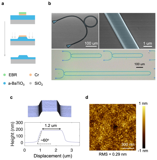
The central object is the etch process itself: Ar+ ion milling with a small Cl2 fraction, run in an inductively coupled plasma reactive ion etching tool with a chromium hard mask on a 340 nm a-oriented BTO film on SiO2. The Ar+ ions provide physical etching, and the Cl2 reacts with sputtered barium and titanium to form volatile byproducts that are pumped away instead of redepositing on the sidewalls. That mechanism directly carries the argument: it converts the usual source of scattering loss, namely sidewall redeposition and roughness, into a residue-free surface, which is what the high $Q_i$ and low propagation loss are attributed to. The quality-factor analysis across racetrack resonators with varying straight fraction, using $\alpha = 2\pi n_g/(Q_i \lambda) \cdot 10\log_{10} e$, then separates straight-waveguide loss from bending loss.
What would settle it
Remeasure the linewidth of the same 200 micrometre racetrack and convert to propagation loss using a group index independently determined from the resonator free spectral range; if the resulting $\alpha$ is not within the reported statistical spread around 0.32 dB/cm, the headline loss is an artifact of the assumed $n_g$. Alternatively, fabricate identical waveguides with the Cl2 flow turned off: if the intrinsic Q does not drop when sidewall redeposition returns, the etch is not the cause of the low loss.
Extended reading notes
Core claim
The paper's central claim is that adding a small fraction of Cl2 gas to Ar+ ion milling makes monolithic BTO etching redeposition-free, producing sidewalls that are smooth (0.29 nm rms) and sufficiently vertical (about 60 degrees), and that this fabrication advance is what allows BTO microresonators to reach intrinsic quality factors above 1 million for the first time. The authors report $Q_i = 1.35 \times 10^6$ for a 200 micrometre-turn-radius microracetrack, $Q_i = 0.84 \times 10^6$ for a 50 micrometre-radius ring, and a straight-waveguide propagation loss extrapolated to about 0.3 dB/cm, with 0.32 dB/cm as the best individual measurement. They also report that common wet-cleaning chemistries (RCA-1, hot piranha, KOH, buffered oxide etch) either damage BTO or fail to remove redeposited material, which is why the redeposition-free etch matters. The electro-optic demonstration supports the platform's purpose: a single-arm Mach-Zehnder interferometer with $V_\pi = 1.44$ V and $V_\pi L = 0.54$ V$\cdot$cm, corresponding to $r_{\mathrm{eff}} \approx 162$ pm/V.
Load-bearing premise
The entire loss and quality-factor report rests on the conversion from measured resonance linewidths to intrinsic Q and propagation loss using a coupling model and a group index $n_g$ that the paper does not state, so any error in those inputs scales the headline numbers proportionally.
Editorial extensions
If this is right
- BTO microresonators can hold photons for roughly a nanosecond at telecom wavelengths, which makes resonant nonlinear optics and electro-optic modulation practical in a monolithic platform.
- The same etch produces a single-arm Mach-Zehnder modulator with $V_\pi L = 0.54$ V$\cdot$cm, so low switching voltage and low propagation loss no longer require a hybrid silicon or silicon-nitride host.
- The loss values place BTO within reach of applications the paper enumerates: electro-optic and Kerr frequency combs, higher harmonic generation, narrow-linewidth lasers, and squeezed light sources.
- Because the process avoids damaging wet cleans, it sidesteps the Curie-temperature constraint that made high-temperature residue removal impractical for BTO.
Reading between the lines
- A direct dispersion measurement, for example from the resonator free spectral range, would supply $n_g$ explicitly; without it, the 0.32 dB/cm figure inherits any error in the assumed group index, since the quoted loss scales linearly with $n_g$.
- If the same Ar+Cl2 chemistry works for other perovskite oxides whose etch products are involatile, it could generalize the redeposition-free sidewall result beyond BTO.
- A test that separates sidewall scattering from material absorption, for example by varying waveguide width or measuring quality factor versus temperature, would show whether further loss reduction should come from etch refinement or from film quality.
- Switching from planar poling at 120 V to sidewall electrodes could raise the effective electro-optic coefficient closer to bulk BTO values, making the modulator figure of merit even stronger.
Editorial analysis
A structured set of objections, weighed in public.
Referee Report
Summary. The manuscript reports a redeposition-free Ar+Cl2 dry etching process for monolithic barium titanate (BTO)-on-insulator waveguides, and uses it to fabricate microracetrack and microring resonators. The central claims are an intrinsic quality factor Qi = 1.35×10^6 (the first >1 million in BTO), a propagation loss as low as 0.32 dB/cm, and Mach–Zehnder modulators with VπL = 0.54 V·cm and an effective Pockels coefficient r_eff = 162 pm/V. The paper motivates the etch chemistry by showing that conventional wet cleans (RCA-1, piranha, KOH, BOE) are ineffective or damaging for BTO, whereas the Ar+Cl2 process yields smooth, vertical sidewalls with ~0.29 nm rms roughness. Loss values are extracted from resonance linewidths across many devices and resonances, and the straight-waveguide loss is extrapolated to ≈0.3 dB/cm from a series of racetracks with varying straight fraction.
Significance. If the reported results hold, this is a significant advance for BTO integrated photonics: it would remove a key fabrication bottleneck (sidewall roughness and residue) and demonstrate that long photon lifetimes are achievable in a strong electro-optic material. The statistical analysis over many resonances and the benchmarking against prior BTO platforms are strengths, as is the practical etch improvement that may transfer to other ferroelectric oxides. However, the headline claims depend on two unstated inputs—the coupling model used to separate Qi from QL and the group index ng used to convert Qi to loss—and on an unreported overlap integral for the r_eff extraction. These gaps must be closed for the record claims to be fully verifiable.
major comments (3)
- [Optical characterization, Fig. 2a] The reported Qi = 1.35×10^6 and QL = 0.8×10^6 are extracted from a single transmission resonance, but the manuscript does not state the coupling model used to separate intrinsic from loaded quality factor. It only says the device is 'near-critical coupling.' Please provide the resonance fitting function, the coupling Qc (or the resonance extinction ratio), and the uncertainty on Qi. This is load-bearing because a mis-assigned coupling state could shift Qi by tens of percent and would directly affect the '>1 million' headline claim.
- [Optical characterization, Fig. 2d] The conversion from Qi to loss uses α = 2πng/(Qiλ)·10log10 e, where the group index ng is never stated or measured. Since the loss scales linearly with ng, a 10% error in ng changes 0.32 dB/cm to about 0.35 dB/cm, so the quoted loss carries a proportional systematic uncertainty that is not quantified. Please report the value of ng used (with its source, e.g., a mode simulation or an independent measurement) and its uncertainty. In addition, the text and Fig. 2d treat the racetrack loss as uniform; the quoted 0.32 dB/cm is therefore a length-weighted average over straight and bent sections, not the straight-waveguide loss, which is separately extrapolated to ≈0.3 dB/cm. This distinction should be stated explicitly wherever the 0.32 dB/cm figure appears.
- [Electro-optic modulation analysis, r_eff extraction] The effective Pockels coefficient r_eff = 162 pm/V is obtained from r_eff = λg/(n^3 Γ VπL), but the overlap integral Γ is not reported, and the assumed refractive index n = 2.26 is given without uncertainty. Please provide the simulated Γ value (with simulation details) and the uncertainty in the Vπ measurement. Without Γ, the reader cannot independently verify the r_eff claim, which is one of the paper's three headline results.
minor comments (5)
- [Fig. 1 caption] The caption says 'Electro-beam lithography'; this should be 'Electron-beam lithography.'
- [Supplementary S1] The phrase 'whose the etch recipe is similar' contains a grammatical error; it should read 'whose etch recipe is similar.'
- [Fig. 2c,d] The error bars are described as statistical variation over resonances, but the number of devices measured per data point is not stated; please specify how many devices and how many resonances contribute to each point.
- [Fig. 2e and Table S1] The benchmarking spans a wide range of wavelengths (632–1577 nm); since propagation loss is wavelength-dependent, a brief note on this caveat would make the comparison fairer and more informative.
- [Abstract and main text] The phrase 'waveguide propagation loss as small as 0.32 dB/cm' could be misread by nonspecialists as the straight-waveguide loss. Consider rewording to 'racetrack effective propagation loss' or 'best measured propagation loss (including bend sections)' to avoid ambiguity.
Circularity Check
No significant circularity: the intrinsic Q, loss, and reff values are measured or extracted by standard, independently stated formulas rather than being reintroduced as predictions.
full rationale
The paper's central claims are experimental measurements. The intrinsic Qi = 1.35e6 and loaded QL = 0.80e6 for the racetrack are obtained from measured transmission resonances (Fig. 2a), and the 0.32 dB/cm loss is converted from the same individual Qi via the standard relation alpha = 2*pi*ng/(Qi*lambda)*10*log10(e), where ng and lambda are the only inputs; this is an extraction, not a fit. The separate straight-waveguide loss estimate of about 0.3 dB/cm is a linear extrapolation of the measured Qi versus straight-fraction series (Fig. 2d) and is explicitly labeled as an extrapolation, so it is not presented as an independent prediction. The effective electro-optic coefficient reff = 162 pm/V is computed from a measured Vpi*L = 0.54 V*cm through the standard formula reff = lambda*g/(n^3*Gamma*Vpi*L), with the simulation-based overlap Gamma and assumed n = 2.26; the formula is not inverted to manufacture Vpi*L. The only self-citations ([S1], [S2] for a LiNbO3 etch recipe used as a comparison in Supplementary S1) are not load-bearing for the BTO process or the Q/loss claims. Unreported details such as ng and the coupling-state model are reproducibility gaps, not circularity.
Assumptions & free parameters
free parameters (3)
- group index ng =
not stated in text
- overlap integral Γ =
not stated, from FEA simulation
- straight and bend loss fit parameters =
straight 0.3 dB/cm, bend 0.48 to 0.53 dB/cm
assumptions (4)
- domain assumption Resonance dip analysis assumes a Lorentzian lineshape with a known coupling state (near-critical), allowing separation of intrinsic and loaded Q.
- domain assumption The Ar+Cl2 etch leaves no optically absorbing residue or subsurface damage; only SEM and AFM imaging are used to support this claim.
- domain assumption The BTO refractive index n=2.26 at 1550 nm and the Pockels tensor components from prior literature are valid for the fabricated film.
- domain assumption Poling at 120 V for 30 minutes produces a single-domain [011] orientation in the measured device.
Cite this review
Pith. "Pith review of Low loss monolithic barium titanate on insulator integrated photonics with intrinsic quality factor >1 million." pith.science (2026). https://pith.science/paper/S2OTDY5H
@misc{pith2026250717150,
  author       = {Pith},
  title        = {Pith review of: Low loss monolithic barium titanate on insulator integrated photonics with intrinsic quality factor >1 million},
  year         = {2026},
  howpublished = {\url{https://pith.science/paper/S2OTDY5H}},
  note         = {Machine review of arXiv:2507.17150}
}
abstract
Barium titanate (BTO) has been experiencing a surge of interest for integrated photonics technologies because of its large nonlinear optical coefficients, especially the Pockels coefficient, and in part due to newly available thin-film substrates. In this work, we report on the development of a redeposition-free dry etching technique for monolithic BTO-on-insulator photonics, that produces very low-roughness and high-verticality waveguides. Using this, we experimentally demonstrate the first BTO microresonators with intrinsic Q-factor $> 1$ million, and waveguide propagation loss as small as 0.32 dB/cm, representing the lowest losses reported in any BTO-based integrated platform to date. We additionally demonstrate Mach-Zehnder amplitude modulators with $V_{\pi}L = 0.54$ V$\cdot$cm and effective electro-optic coefficient $r_\text{eff} = 162$ pm/V.
Figures


Forward citations
Cited by 2 Pith papers
-
Monolithic Barium Titanate Nanophotonics and Electro-optics
Monolithic BTOI photonic crystals and Fabry–Pérot cavities reach ~0.5 dB/cm loss, Q up to 230k, reff ≈ 154 pm/V, and ~11 GHz material-limited EO bandwidth at the PhC band edge.
-
Electro-Optic Active Metasurfaces for High-Speed Photonic Applications
A field review of electro-optic metasurfaces that organizes the literature into four material platforms and six resonance-enhancement mechanisms, with comparative performance tables and an application survey.
Reference graph
Works this paper leans on
-
[1]
Johnston, A. & Weingart, J. Determination of the Low-Frequency Linear Electro-Optic Effect in Tetragonal BaTiO3. Journal of the Optical Society of America 55, 828–834 (1965)
work page 1965
-
[2]
Abel, S. et al. A Hybrid Barium Titanate–Silicon Photonics Platform for Ultraefficient Electro-Optic Tuning. Journal of Lightwave Technology34, 1688–1693 (2016)
work page 2016
-
[3]
Eltes, F. et al. Low-Loss BaTiO3 –Si Waveguides for Nonlinear Integrated Photonics. ACS Photonics 3, 1698–1703 (2016). 7
work page 2016
-
[4]
Abel, S. et al. Large Pockels effect in micro- and nanostructured barium titanate integrated on silicon. Nature Materials 18, 42–47 (2019)
work page 2019
-
[5]
Eltes, F. et al. A BaTiO3-Based Electro-Optic Pockels Modulator Mono- lithically Integrated on an Advanced Silicon Photonics Platform. Journal of Lightwave Technology37, 1456–1462 (2019)
work page 2019
-
[6]
Posadas, A. B., Stenger, V. E., DeFouw, J. D., Warner, J. H. & Demkov, A. A. RF-sputtered Z-cut electro-optic barium titanate modulator on sili- con photonic platform. Journal of Applied Physics134, 073101 (2023)
work page 2023
-
[7]
Tao, M. et al.Towards high quality transferred barium titanate ferroelectric hybrid integrated modulator on silicon. Light: Advanced Manufacturing5, 1 (2024)
work page 2024
-
[8]
Ortmann, J. E. et al. Ultra-Low-Power Tuning in Hybrid Barium Ti- tanate–Silicon Nitride Electro-optic Devices on Silicon. ACS Photonics 6, 2677–2684 (2019)
work page 2019
Show all 36 references
-
[9]
Eltes, F. et al. An integrated optical modulator operating at cryogenic temperatures. Nature Materials 19, 1164–1168 (2020)
2020
-
[10]
Posadas, A. B. et al. Thick BaTiO 3 Epitaxial Films Integrated on Si by RF Sputtering for Electro-Optic Modulators in Si Photonics. ACS Applied Materials & Interfaces13, 51230–51244 (2021)
2021
-
[11]
Kohli, M. et al. Plasmonic Ferroelectric Modulator Monolithically Inte- grated on SiN for 216 GBd Data Transmission. Journal of Lightwave Tech- nology 41, 3825–3831 (2023)
2023
-
[12]
Reynaud, M. et al. Microstructural analysis and electro-optic properties of thick epitaxial BaTiO 3 films integrated on silicon (001). Physical Review Materials 6, 095201 (2022)
2022
-
[13]
Guo, W., Posadas, A. B. & Demkov, A. A. Epitaxial integration of Ba- TiO3 on Si for electro-optic applications. Journal of Vacuum Science & Technology A: Vacuum, Surfaces, and Films39, 030804 (2021)
2021
-
[14]
& Buchal, C
Petraru, A., Schubert, J., Schmid, M. & Buchal, C. Ferroelectric BaTiO3 thin-film optical waveguide modulators. Applied Physics Letters81, 1375– 1377 (2002)
2002
-
[15]
Dong, Z. et al. Monolithic Barium Titanate Modulators on Silicon-on- Insulator Substrates. ACS Photonics 10, 4367–4376 (2023)
2023
-
[16]
Raju, A. et al. High-Q Monolithic Ring Resonators in Low-Loss Barium Titanate on Silicon. Laser & Photonics Reviews2402086 (2025)
2025
-
[17]
et al.Barium titanate and lithium niobate permittivity and Pockels coefficients from megahertz to sub-terahertz frequencies
Chelladurai, D. et al.Barium titanate and lithium niobate permittivity and Pockels coefficients from megahertz to sub-terahertz frequencies. Nature Materials 24, 868–875 (2025). 8
2025
-
[18]
Riedhauser, A. et al. Absorption loss and Kerr nonlinearity in barium titanate waveguides. APL Photonics 10, 016121 (2025)
2025
-
[20]
Isti, M. I. A. et al. Fabrication and Optical Characterization of Low- Loss Barium Titanate Waveguides. IEEE Photonics Technology Letters 37, 1101–1104 (2025)
2025
-
[21]
& Kim, N.-Y
Li, Y., Wang, C., Yao, Z., Kim, H.-K. & Kim, N.-Y. Comparative analysis of barium titanate thin films dry etching using inductively coupled plasmas by different fluorine-based mixture gas. Nanoscale Research Letters9, 530 (2014)
2014
-
[22]
Cheng, J. et al. Nanoscale etching of perovskite oxides for field effect transistor applications. Journal of Vacuum Science & Technology B, Nan- otechnology and Microelectronics: Materials, Processing, Measurement, and Phenomena 38, 012201 (2020)
2020
-
[23]
& Bernal, M.-P
Ulliac, G., Calero, V., Ndao, A., Baida, F. & Bernal, M.-P. Argon plasma inductively coupled plasma reactive ion etching study for smooth sidewall thin film lithium niobate waveguide application. Optical Materials 53, 1–5 (2016)
2016
-
[24]
Wang, C. et al. Lithium tantalate photonic integrated circuits for volume manufacturing. Nature 629, 784–790 (2024)
2024
-
[25]
Younesi, M. et al. Fabrication of low-loss lithium niobate on insulator waveguides on the wafer scale. Optical Materials Express15, 299 (2025)
2025
-
[26]
Demkov, A. A. & Posadas, A. B. Ferroelectric BaTiO 3 for Electro-Optic Modulators in Si Photonics. IEEE Journal of Selected Topics in Quantum Electronics 30, 1–13 (2024)
2024
-
[27]
B., Wilson, A
Posadas, A. B., Wilson, A. B. & Demkov, A. A. Effect of poling voltage on electro-optic response of epitaxial BaTiO 3 on Si grown by sputtering. In 2024 IEEE Silicon Photonics Conference (SiPhotonics), 1–2 (IEEE, Tokyo Bay, Japan, 2024)
2024
-
[28]
Franken, C. A. A. et al. Milliwatt-level UV generation using sidewall poled lithium niobate (2025). ArXiv:2503.16785 [physics]
2025 arXiv
-
[29]
Zhang, M. et al. Broadband electro-optic frequency comb generation in a lithium niobate microring resonator. Nature 568, 373–377 (2019)
2019
-
[30]
Del’Haye, P. et al. Optical frequency comb generation from a monolithic microresonator. Nature 450, 1214–1217 (2007). 9
2007
-
[31]
& Jarrahi, M
Moore, J., Tomes, M., Carmon, T. & Jarrahi, M. Continuous-wave cascaded-harmonic generation and multi-photon Raman lasing in lithium niobate whispering-gallery resonators. Applied Physics Letters99, 221111 (2011)
2011
-
[32]
Jin, W. et al. Hertz-linewidth semiconductor lasers using CMOS-ready ultra-high-Q microresonators. Nature Photonics 15, 346–353 (2021)
2021
-
[33]
Safavi-Naeini, A. H. et al. Squeezed light from a silicon micromechanical resonator. Nature 500, 185–189 (2013)
2013
-
[34]
Ahmed, S. R. et al. Universal photonic artificial intelligence acceleration. Nature 640, 368–374 (2025)
2025
-
[35]
Ou, S. et al. Hypermultiplexed integrated photonics–based optical tensor processor. Science Advances11, 11 (2025)
2025
-
[36]
Liu, W. et al. A fully reconfigurable photonic integrated signal processor. Nature Photonics 10, 190–195 (2016)
2016
-
[37]
Prabhathan, P. et al. Roadmap for phase change materials in photonics and beyond. iScience 26, 107946 (2023). Acknowledgments The authors would like to acknowledge invaluable support from Dr. Edmond Chow and Dr. Soo Ho Choi at the Holonyak Micro & Nanotechnology Lab at the Uni...
2023 arXiv
Reviewed August 6, 2026 · model on record in the stance chip above.
Discussion (0). Continue with ORCID to comment.