REVIEW 3 major objections 5 minor
Electron transport in a 1.6~nm-thick double-gated (100) silicon nanosheet: A theoretical study accounting for phonon confinement and remote-phonon scattering
T0 review · 3 major / 5 minor · reviewed 2026-08-16 · deepseek-v4-flash
Pith's one-line read For a 1.6 nm double-gated (100) silicon nanosheet, phonon confinement and interface plasmon-phonon scattering set the room-temperature mobility near 200–360 cm²/Vs and can lower the saturation velocity below bulk silicon.
desk verdict A careful full-band Monte Carlo study whose main qualitative result—low saturation velocity from transfer into flat primed subbands—is likely right, while the quantitative mobility numbers depend on an approximate phonon boundary-condition model that needs independent validation. read the letter →
The pith
A machine-rendered reading of the paper's core claim, the machinery that carries it, and where it could break.
The reading
What carries the argument
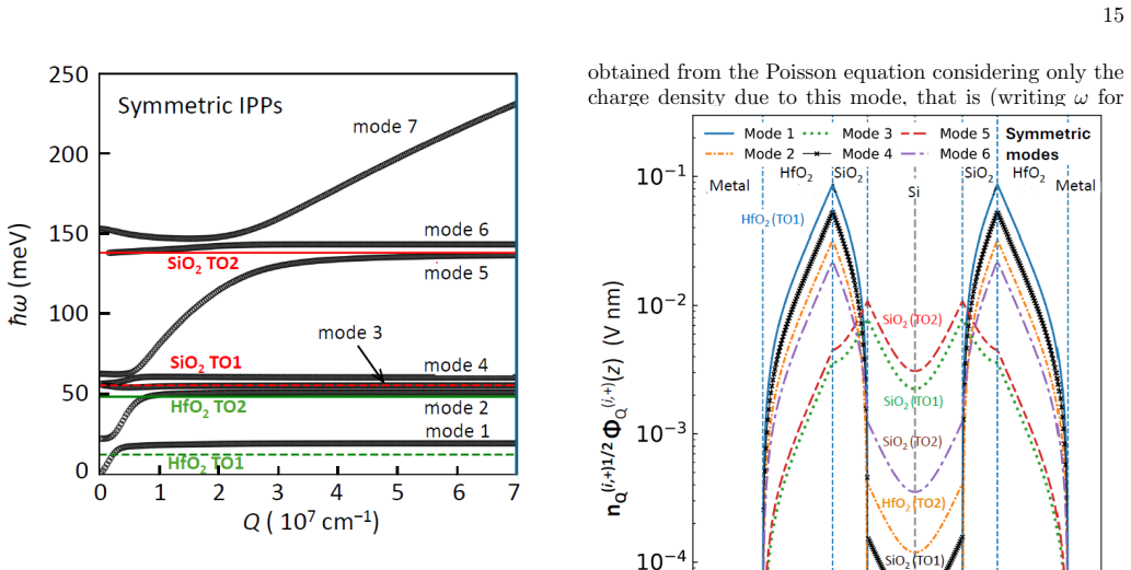
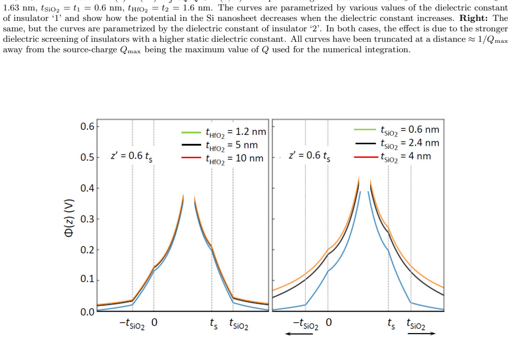
The load-bearing object is the elastic-continuum model of confined acoustic phonons, with branch-specific quantized transverse wave vectors $q_{z,m}=m\pi/(t_s+2z_0)$, where $t_s$ is the sheet thickness and $z_0$ is an effective penetration depth of the vibration into the SiO₂ layers, fixed by stress continuity at the interfaces. The electron-phonon coupling is carried by shape functions $G_m(z)$ derived from the divergence of the ionic displacement field; different boundary conditions — free-standing, clamped at Si/SiO₂, clamped at SiO₂/HfO₂ — change these shape functions and the number and zero-point energy of the acoustic branches. The second mechanism is the dielectric-continuum treatment of interface plasmon-phonon modes, where a secular equation yields symmetric and antisymmetric hybrid-mode dispersions and the scattering potential is quantized by equating the time-averaged field energy to the oscillator ground-state energy. A full-band empirical-pseudopotential band structure and a Monte Carlo transport solver complete the machinery, so the flat primed-subband dispersion that controls the saturation velocity is resolved directly rather than through an effective-mass approximation.
What would settle it
Measure the low-field electron mobility of a 1.6 nm double-gated (100) Si nanosheet with the exact 0.6 nm SiO₂/1.2 nm HfO₂ stack; a value well above $360\ \mathrm{cm^2/Vs}$ would show that the clamped outer-interface model over-suppresses phonon scattering. A complementary atomistic calculation of the phonon dispersions and electron-phonon couplings for the same stack would settle whether the elastic-continuum clamping picture is quantitatively correct.
Extended reading notes
Core claim
The central claim is that phonon confinement, not just electron confinement, controls transport in a 1.6 nm silicon nanosheet. Depending on how the confined acoustic phonons are pinned, the room-temperature mobility ranges from about $160\ \mathrm{cm^2/Vs}$ (free-standing boundary conditions at the Si/SiO₂ interfaces) to about $1060\ \mathrm{cm^2/Vs}$ (clamped at the Si/SiO₂ interfaces). The physically motivated choice — acoustic phonons clamped at the stiff outer SiO₂/HfO₂ interfaces, optical phonons clamped at the Si/SiO₂ interfaces — gives $260\ \mathrm{cm^2/Vs}$ unscreened and $360\ \mathrm{cm^2/Vs}$ with dielectric screening, instead of the $700\ \mathrm{cm^2/Vs}$ of the bulk-phonon elastic approximation. Scattering with interface hybrid plasmon-phonon modes reduces the low-field mobility to about $200\ \mathrm{cm^2/Vs}$ at $1.15\times10^{13}\ \mathrm{cm^{-2}}$ sheet density, yet because these inelastic small-angle collisions keep electrons cool, the saturated drift velocity reaches above $2\times10^7\ \mathrm{cm/s}$. Without those modes, the saturation velocity is $5.5\times10^6\ \mathrm{cm/s}$ ($8.9\times10^6\ \mathrm{cm/s}$ screened), below the bulk value, because electrons transfer at high field into the flat fourfold-degenerate primed subband ladder — an explanation the authors present for previously measured but unexplained low inversion-layer saturation velocities.
Load-bearing premise
The quantitative headline rests on the assumption that acoustic vibrations are pinned at the outer SiO₂/HfO₂ interfaces and can be described by a single approximate penetration depth for every branch; if the true interface condition is different, the computed mobility shifts between about $160\ \mathrm{cm^2/Vs}$ and $1060\ \mathrm{cm^2/Vs}$.
Editorial extensions
If this is right
- For the 1.6 nm double-gated stack, the phonon-limited room-temperature mobility is predicted to be about $260\ \mathrm{cm^2/Vs}$ unscreened and $360\ \mathrm{cm^2/Vs}$ with dielectric screening, not the $\sim 700\ \mathrm{cm^2/Vs}$ bulk-phonon value.
- The high-field saturation velocity is below the bulk value ($\sim 5.5\times10^6\ \mathrm{cm/s}$ unscreened, $\sim 8.9\times10^6\ \mathrm{cm/s}$ screened) because electrons transfer into the flat primed subbands; this supplies a theoretical explanation for old inversion-layer measurements.
- Interface plasmon-phonon scattering lowers the low-field mobility to about $200\ \mathrm{cm^2/Vs}$ but raises the saturated velocity above $2\times10^7\ \mathrm{cm/s}$, so high-κ gate stacks need not degrade nanosheet transistors.
- The mobility depends only weakly on electron density and gate bias in these ultra-thin sheets, because the external potential barely perturbs the band structure even at $10^{13}\ \mathrm{cm^{-2}}$ sheet density.
Reading between the lines
- Relaxing the mode-independent penetration-depth approximation — letting $z_0$ vary per branch or per polarization — could shift the relative weights of dilatational versus flexural scattering and is a testable refinement of the model.
- An atomistic phonon calculation for the same SiO₂/HfO₂ stack would test the clamping assumption; if interfacial stiffness is softer than assumed, the mobility could move toward the upper part of the 160–1060 cm²/Vs bracket.
- The predicted high-field benefit of IPP scattering suggests short-channel transistors, where transport is more streaming-like, could show a larger relative velocity boost than the long-channel mobility alone indicates.
- Since the model predicts weak mobility dependence on electron density, a density sweep in a 1.6 nm double-gate device could separate intrinsic phonon-limited behavior from extrinsic interface-roughness and charge-defect scattering.
Signed reviews
Editorial analysis
A structured set of objections, weighed in public.
Referee Report
Summary. The paper reports a full-band Monte Carlo study of low-field mobility and high-field drift velocity in a 1.6 nm-thick double-gated (100) Si nanosheet with SiO2/HfO2 gate stacks. The electron band structure is obtained from local empirical pseudopotentials, confined acoustic phonons are described by an elastic continuum model under three boundary-condition choices, and interface plasmon-phonon (IPP) scattering is treated in the dielectric continuum limit. The central quantitative claims are that the realistic assumption of acoustic phonons clamped at the SiO2/HfO2 interfaces yields a room-temperature phonon-limited mobility of about 260 cm2/Vs (360 cm2/Vs with static dielectric screening and about 200 cm2/Vs with IPP scattering), much lower than the 700 cm2/Vs obtained with bulk phonons in the elastic high-temperature approximation; that the saturation velocity is reduced below the bulk value because electrons transfer into the flat primed subbands; and that IPP scattering, while lowering the low-field mobility, increases the saturation velocity.
Significance. If the quantitative results are robust, the paper provides a plausible explanation for the long-standing observation of reduced saturation velocity in Si inversion layers and a careful account of remote-phonon effects in extremely scaled nanosheet transistors. The strengths include the use of full-band pseudo-potential electronic structure, explicit treatment of the hybridization of 2DEG plasmons with insulator optical phonons, selection rules for IPP scattering, and a comparison with available experimental data for ultra-thin Si films. However, the headline mobility and velocity numbers rest on an approximate elastic-continuum phonon-confinement model whose key parameter, the penetration depth z0, is replaced by a single m-independent value while the manuscript itself states that the exact roots of Eq. (20) vary between 49% and 91% of that value. Since Table III shows that the mobility changes by a factor of about 6.6 across boundary-condition choices, the central numerical claims are not yet anchored without a sensitivity analysis. No code or tabulated data are provided to make the numerical results independently checkable.
major comments (3)
- [Sec. III.B, Eq. (20)] The m-independent replacement z0 ≈ t1(c_Si/c_SiO2)^2 is load-bearing for the headline mobility values. The text states that the smallest roots of Eq. (20) for m = 1..16 lie between 49% and 91% of this adopted value, and Eqs. (21)-(23) as well as the number of acoustic branches (~16) depend directly on z0. Because Table III shows that the mobility varies from 160 to 1060 cm2/Vs depending on the boundary-condition choice, a factor-of-two uncertainty in z0 can plausibly shift the central 260/360/200 cm2/Vs numbers by tens of percent. Please recompute the low-field mobility and saturation velocity using the exact branch-dependent roots of Eq. (20), or at least provide a sensitivity study over the stated 0.49-0.91 range, and report how the conclusions change.
- [Sec. VI, Table III] The comparison between the 'realistic' CBC@SiO2/HfO2 results and the bulk-phonon value of 700 cm2/Vs conflates two separate approximations: the choice of phonon boundary conditions and the static-screening approximation. The manuscript acknowledges in Sec. IV that static screening is expected to give an upper bound for the mobility, but no uncertainty estimate is attached to the quoted 260/360/200 cm2/Vs values. Because the physical choice of clamped boundary conditions at SiO2/HfO2 is argued from elasticity tables rather than validated against experiment or atomistic simulation for this specific 1.6 nm geometry, the quantitative strength of the claim that the realistic mobility is 'much smaller' than the bulk value needs to be demonstrated by showing the range of mobility obtained when the elastic parameters in Table I and the screening model are varied within their accepted uncertainties.
- [Sec. III.B, Eqs. (21)-(23)] The normalization constant Nm in Eqs. (21) and (22) is approximated by the m-independent form in Eq. (23) in the same spirit as the z0 approximation. This approximation enters directly into the deformation-potential matrix element of Eq. (25), and its accuracy is not separately checked. Since the claimed reduction of the electron-phonon coupling relies on the increased effective mass density of the Si/SiO2 sandwich, a quantitative check of Eq. (23) against the full expression in Eq. (22) for the relevant m values should be reported.
minor comments (5)
- [Throughout] There are numerous typographical errors that should be corrected, e.g., 'fogr' after Eq. (23), 'SO2' instead of 'SiO2' in Sec. III.B and in the Fig. 10 caption, 'cmn/s' in Sec. VII, and 'A pgpl' in Ref. [63].
- [Sec. VI] The phrase 'a high-kappainsulator' in the discussion of Table III is missing a space and should read 'a high-kappa insulator'.
- [Sec. VI, Fig. 11 and Table III] The saturated-velocity values are given as '≳5.6' and '≳8.9' in Table III, but the text quotes specific values (5.5×10^6 and 8.9×10^6 cm/s). Please make the reporting consistent and clarify whether the tabulated entries are lower bounds or converged Monte Carlo estimates.
- [Sec. IV, Eq. (32)] The static-screening correction in Eq. (33) is acknowledged to be an approximation, but the direction of the error is stated only qualitatively as 'presumably obtaining a lower bound for the scattering rates.' It would be helpful to state explicitly whether the screened form factor is always ≤1 for the matrix elements used, because the Monte Carlo implementation relies on this inequality.
- [Conclusions] The statement that the results for the saturated velocity are 'the first to predict' the lower experimental values would be easier to evaluate if the paper briefly explained why the earlier effective-mass-based Monte Carlo studies cited in Refs. [84]-[88] failed to capture the primed-subband effect, given that the primed-subband dispersion was already known in that literature.
Circularity Check
No significant circularity: the phonon-confinement and IPP models are independently parameterized inputs; the mobility and velocity results are computed outputs.
full rationale
The paper's central numerical claims are not equivalent to any fitted input. The electron dispersion is computed from empirical pseudopotentials, the acoustic-phonon confinement parameters come from an elastic-continuum model whose material constants are taken from the bulk literature (Table I and Table II), and the IPP scattering rates are computed from a standard dielectric-continuum quantization with independently specified dielectric functions. No free parameter is fitted to reproduce the nanosheet mobility or saturated velocity. The z0 approximation in Sec. III.B is an acknowledged modeling approximation: the paper explicitly states that the exact roots of Eq. (20) vary between 49% and 91% of the adopted asymptotic value, and Table III exposes a roughly 6.6x sensitivity to boundary-condition choice. This is an uncertainty and sensitivity statement, not a disguised fit: the headline 260/360/200 cm2/Vs values are outputs of the model, not targets used to select z0. Self-citations to Refs. [30], [31], and [88] provide framework, dimensionality arguments, and historical context, but the load-bearing deformation potentials, phonon energies, sound velocities, and experimental comparisons are drawn from external sources or are clearly stated as model assumptions. No uniqueness theorem is imported to forbid alternatives, and the paper candidly notes that experimental data are scant and that 'we cannot draw any exact quantitative conclusion.' Thus the derivation chain is self-contained relative to its inputs; the main risks are modeling accuracy of the confinement boundary conditions, which is a scientific uncertainty rather than circularity.
Assumptions & free parameters
free parameters (6)
- Acoustic deformation potentials (Delta_dil=10 eV, Delta_flex=2 eV) =
10 eV and 2 eV
- Optical deformation potential (DK)_op =
1.75e8 eV/cm
- Phonon zone-edge energies =
Dilatational 49.5 meV, flexural 33 meV, LO 66/49.5 meV, TO 66/64 meV
- Confined-phonon penetration depth z0 =
Roughly 2.5t1 (dilatational) and 3.1t1 (flexural), with t1=0.6 nm
- Number of confined acoustic modes =
16 dilatational, 16 flexural, 48 total acoustic
- Electron sheet density for the IPP case =
1.15e13 cm-2
assumptions (6)
- domain assumption Elastic continuum approximation for confined acoustic phonons
- domain assumption Clamped boundary conditions at SiO2/HfO2 interfaces are physically realistic
- domain assumption Local empirical pseudopotentials give accurate band structure for H-terminated Si nanosheets
- domain assumption Scalar 2DEG dielectric response and approximate Landau damping
- ad hoc to paper Static screening of electron-phonon interactions is a valid lower-bound approximation
- domain assumption Ideal metal gates and symmetric gate stacks
Cite this review
Pith. "Pith review of Electron transport in a 1.6~nm-thick double-gated (100) silicon nanosheet: A theoretical study accounting for phonon confinement and remote-phonon scattering." pith.science (2026). https://pith.science/paper/SEKOT54E
@misc{pith2026260812214,
  author       = {Pith},
  title        = {Pith review of: Electron transport in a 1.6~nm-thick double-gated (100) silicon nanosheet: A theoretical study accounting for phonon confinement and remote-phonon scattering},
  year         = {2026},
  howpublished = {\url{https://pith.science/paper/SEKOT54E}},
  note         = {Machine review of arXiv:2608.12214}
}
read the original abstract
We study theoretically electron transport in an top-and bottom-gated (100) 1.6 nm-thin silicon nanosheet with SiO2/HfO2 gate stacks, focusing on the intrinsic physical processes that affect transport: the confinement of phonons and the presence of interface hybrid plasmon-phonon excitations (IPPs or `remote phonons'). The band structure is calculated using local empirical pseudopotentials; an approximated elastic continuum model is used to consider the confinement of acoustic phonons; the dielectric continuum limit is used to deal with the IPPs. We find that the electron mobility is affected significantly by the boundary conditions chosen to deal with phonon confinement. The more realistic assumption of phonons clamped at the SiO2/HfO2 interfaces and optical phonons at the Si/SiO2 interfaces results in a room temperature mobility much smaller than what is obtained using the common assumption of bulk phonons in the elastic, high-temperature approximation. We also find that, as a result of the complicated structure of the primed subbands, the high-field saturated velocity is significantly lower than its bulk value, as it had been measured in the past in the case of Si inversion layers but never explained theoretically. Finally, we find that IPP scattering does depress the low-field mobility but to a small extent, thanks to the presence of the interfacial SiO2 layers and to the proximity of the metal gates. Moreover, by keeping electrons `cooler', IPP scattering results in a higher saturated velocity. Therefore, the presence of high-kappa materials in the gate-insulator stacks should not affect negatively the performance of field effect transistors based on Si nanosheets.
Figures


Figures from the paper (11 more)





Reviewed August 16, 2026 · model on record in the stance chip above.
Discussion (0). Continue with ORCID to comment.