REVIEW 4 major objections 4 minor 4 references
The role of graphitic filaments in resistive switching behaviour of amorphous silicon carbide thin films
T0 review · 4 major / 4 minor · reviewed 2026-08-14 · deepseek-v4-flash
Pith's one-line read This paper claims that resistive switching in amorphous silicon carbide memories is carried, in part, by nanocrystalline graphitic filaments that form when the SiC dissociates during switching cycles.
desk verdict A novel but overclaimed observation of graphitic filaments in Pt/Ag a-SiC RRAMs; the formation evidence is solid, the causal contribution to switching is not proven. read the letter →
The pith
A machine-rendered reading of the paper's core claim, the machinery that carries it, and where it could break.
The reading
What carries the argument
The central mechanism is the formation of nanocrystalline graphitic filaments by field-assisted dissociation of amorphous SiC. Local Joule heating melts and dissociates the SiC; metals such as Pt and Cu react with Si to form silicides but not carbides, so carbon segregates and graphitizes into conduction paths aligned with the applied field. Raman D, G, and 2D peaks identify the filaments, and the top-electrode redox potential selects whether metallic or graphitic filaments dominate the switching.
What would settle it
Cycle a Au/SiC/Pt device while measuring Raman or XPS in situ: if graphitic D and G bands appear only after the device permanently fails, or if a device that switches reversibly shows no carbon filament signature in its ON state, the central claim fails. A control experiment with a carbon-free capping layer could also show whether the observed graphite comes from SiC dissociation or from electrode or ambient carbon contamination.
Extended reading notes
Core claim
The paper's central claim is that resistive switching in amorphous SiC is not explained by metallic filaments alone: switching cycles dissociate the SiC itself, and the carbon left behind forms nanocrystalline graphitic filaments that conduct in the ON state. The claim rests on post-cycling characterization: Raman spectra show broad D, G, and 2D bands of nanocrystalline graphite, XPS C1s spectra show sp2 and sp3 carbon components, and cross-sectional SEM shows field-aligned filaments and interdiffused layers that indicate localized melting. The authors state this unambiguously for electrochemically inert top electrodes (Pt and Ag), where they observe 'unambiguous presence of nanocrystalline graphitic filaments,' and argue that for Cu electrodes, where little graphite is found, metallic Cu filaments dominate because Cu's low redox potential makes it dissolve readily. The balance between the two competing mechanisms is set by the electrode's redox potential.
Load-bearing premise
The graphitic carbon seen in Raman and XPS after cycling is the cause of reversible switching, not a byproduct of device breakdown; the paper does not correlate the amount of graphite with a specific memory state.
Editorial extensions
If this is right
- Devices with inert electrodes (Pt and Ag) can still switch, so electrochemical metallization is not a necessary condition for SiC resistive memory.
- The a-SiC switching layer is consumed and reorganized during operation, which sets a finite endurance; devices in this study fail near 50 cycles.
- A 100 nm SiC layer gives the best endurance and high Roff/Ron ratios up to 10^8, with retention above 10^4 s; thinner and thicker layers degrade faster.
- Electrode choice becomes a design lever: low-redox metals favor metallic filaments, while inert metals favor graphitic filaments.
Reading between the lines
- A direct test would be to fabricate a-SiC from 13C-enriched carbon in the sputter target; if the Raman G peak shifts in cycled devices, the filament carbon provably comes from the switching layer rather than from contamination.
- If graphitic filaments store the low-resistance state, seeding the film with a small fraction of graphitic carbon or a carbon-rich interface might lower forming voltage and extend endurance by giving the dissociation a preferential path.
- The dissociation mechanism suggests a bridge to amorphous-carbon and carbon-electrode RRAMs: the switching layer supplies its own filament material, so no external carbon source or electrochemically active electrode is required.
Signed reviews
Editorial analysis
A structured set of objections, weighed in public.
Referee Report
Summary. The manuscript reports resistive switching in amorphous SiC films deposited by single-composite-target RF magnetron sputtering, using an Au bottom electrode and Ag, Cu, or Pt top electrodes with SiC thicknesses of 50, 100, and 300 nm. The authors characterize forming voltages, set/reset voltages and currents, endurance, retention, and ROFF/RON ratios (up to 10^8), and use XRD, cross-sectional SEM, Raman spectroscopy, and XPS to examine structural changes after switching. The central claim, stated in the abstract and summary, is that switching involves dissociation of SiC and the formation of nanocrystalline graphitic filaments for electrochemically inert top electrodes (Pt, Ag), with metallic Cu filaments dominating in Cu devices.
Significance. If the causal interpretation were established, this work would be significant because it proposes a carbon-filament switching mechanism in SiC RRAMs that coexists with electrochemical metallization, with implications for electrode selection and device reliability. The paper has useful strengths: a parametric device matrix across three thicknesses and three top electrodes, identification of 100 nm as optimal thickness, and internally consistent post-mortem evidence (Raman D/G/2D peaks, XPS C=C components, SEM-visible filaments, disappearance of electrode XRD peaks) for graphitic carbon formation in Pt and Ag devices. However, the evidence is ex-situ and not state-resolved, so the current results demonstrate formation of graphitic carbon during or after switching, not its causal role in reversible switching.
major comments (4)
- [Abstract; Results and Discussion (Figs. 9, 10; Fig. S2)] The central claim that graphitic filaments 'contribute to switching' is not supported by the data because all Raman and XPS measurements were made after switching (a few cycles or after endurance testing) and no measurement correlates the amount of graphitic carbon with the instantaneous HRS or LRS state. Fig. S2 shows that endurance testing ends in device failure around 50 cycles, and Figs. 7 and 8 show disappearance of electrode XRD peaks and severe interdiffusion with filament-like protrusions after cycling, so the observed graphite could be a byproduct of terminal device degradation rather than the switching filament. The abstract's statement 'clearly establishes ... These contribute to switching' should be tempered to 'consistent with the formation of graphitic carbon' unless new state-resolved or in-situ evidence is added.
- [Summary; text before Fig. 9] The paper classifies Ag as electrochemically inert and uses the Pt/Ag pair to claim unambiguous graphitic-filament switching for inert electrodes. Ag is a common active electrode in electrochemical metallization cells and can form Ag filaments under bias; this is not addressed. Consequently, the Pt device is the only clean inert-electrode case in the study, and the inference that graphite formation accompanies switching in the absence of electrochemical activity is weakened. The authors should either justify the inertness of Ag in this specific stack or restrict the claim to Pt.
- [Results and Discussion after Fig. 10] For Cu devices, the text states that 'a very small amount of graphite is present' and that conduction is likely due to metallic Cu filaments, but no Raman spectrum for any Cu device is shown and no quantitative comparison of Raman or XPS carbon signals between Cu and Pt/Ag devices is provided. Without this comparative evidence, the claimed difference in switching mechanism between Cu and Pt/Ag is not established.
- [Results and Discussion (Fig. 8)] The SEM images in Fig. 8 show filament-like protrusions and interdiffusion after cycling, but no compositional analysis (e.g., EDS mapping) or spatially resolved Raman/XPS is provided, so the identity of the SEM-visible filaments as graphitic carbon is not demonstrated. The morphological evidence alone cannot distinguish carbon filaments from metallic (e.g., Ag or Cu) filaments or from electrode material that has migrated into the SiC layer.
minor comments (4)
- [Abstract; throughout] Numerical values such as 10^8, 10^4, and 10^6 appear without superscript formatting in several places; the typeset version should ensure these are readable as powers of ten.
- [Raman discussion (Fig. 9)] The sentence 'The presence of large defect activated D peaks in all the decives suggest that a large fraction of the carbon might be sp3 bonded carbon' contains a typo ('decives') and the inference from the D peak to sp3 fraction is not straightforward; Raman D intensity in nanocrystalline graphite is primarily a defect-mode signature and should be discussed with the appropriate references.
- [Table 2 caption] 'Rman peaks' should read 'Raman peaks'.
- [XPS discussion (Fig. 10)] The phrase 'most of the most of the carbon is bonded' contains a duplicated phrase; also, the large C-OH/C-O components are not discussed in relation to the graphitic-filament claim, and the possibility of surface contamination should be addressed.
Circularity Check
No significant circularity: the graphitic-filament claim rests on independent ex-situ Raman and XPS measurements, not on fitted parameters or self-citation.
full rationale
The paper's central claim is that amorphous SiC dissociates during switching and forms nanocrystalline graphitic filaments, detected by Raman and XPS after cycling. This claim is supported by direct ex-situ characterization (Fig. 9 Raman D/G/2D peaks; Fig. 10 C1s XPS components), not by a derivation from the input assumptions. The only self-citation is Ref. 15, which describes the deposition method and is not used as evidence for the filament mechanism, so it is not load-bearing. The conduction-mechanism fits (Schottky, SCLC, Ohmic) are routine curve fitting and do not by construction produce the graphitic-filament conclusion. No fitted parameter is renamed as a prediction; no uniqueness theorem or ansatz is imported from the authors' prior work; no known result is merely renamed. The observation that graphitic carbon is detected only after testing, and the possibility that it is a breakdown byproduct rather than the reversible switching filament, is an evidential weakness about causal interpretation, not a circularity of definition or fitting. The derivation chain therefore remains self-contained with respect to the circularity criteria, and the appropriate score is 0.
Assumptions & free parameters
assumptions (4)
- domain assumption Raman D, G, and 2D peak positions and widths identify nanocrystalline graphite
- domain assumption Joule heating during switching is intense enough to locally melt and dissociate SiC
- domain assumption Post-cycling ex-situ observations reflect the conductive filament structure during switching
- ad hoc to paper Ag is electrochemically inert in this device stack
Cite this review
Pith. "Pith review of The role of graphitic filaments in resistive switching behaviour of amorphous silicon carbide thin films." pith.science (2026). https://pith.science/paper/UU3IG2AV
@misc{pith2026190804079,
  author       = {Pith},
  title        = {Pith review of: The role of graphitic filaments in resistive switching behaviour of amorphous silicon carbide thin films},
  year         = {2026},
  howpublished = {\url{https://pith.science/paper/UU3IG2AV}},
  note         = {Machine review of arXiv:1908.04079}
}
read the original abstract
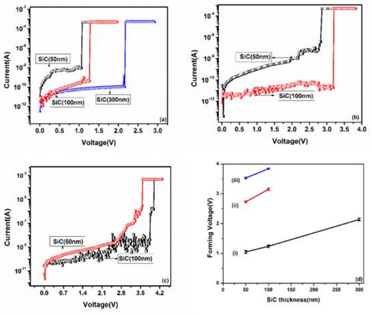
Resistive switching in amorphous silicon carbide (a-SiC) films deposited by a single composite target magnetron sputtering process is reported. Switching performance as a function of thickness of the films (50, 100 and 300 nm) as well as different top metal electrodes (Cu, Pt and Ag) with the bottom electrode fixed as Au, is investigated. The switching parameters (Forming Voltage, Set and Reset voltages and corresponding currents) are found to be dependent on thickness of SiC films and it is observed that 100 nm is the optimal thickness for best endurance. The interface between metal electrode and a-SiC films plays a more significant role in achieving switching performance. Resistance Off/On ratios of 108, retention times >104 s and endurance of 50 cycles are achieved in the best devices. Cross-sectional scanning electron microscopy provides evidence that the mechanism of switching involves the formation of carbonaceous filaments and Raman spectroscopy indicates that these filaments are nanocrystalline graphite in nature. The current work clearly establishes that there is dissociation of SiC during the switching cycles leading to formation of nanocrystalline graphitic filaments. These contribute to switching, in addition to the metallic filaments, in the a-SiC based resistive memory device.
Figures
Reference graph
Works this paper leans on
-
[2]
(28) Merlen, A.; Buijnsters, J.; Pardanaud, C.; Merlen, A.; Buijnsters, J
Nano Lett.2008, 8 (12), 4320–4325. (28) Merlen, A.; Buijnsters, J.; Pardanaud, C.; Merlen, A.; Buijnsters, J. G.; Pardanaud, C. A Guide to and Review of the Use of Multiwavelength Raman Spectroscopy for Characterizing Defective Aromatic Carbon Solids: From Graphene to Amorphous Carbons. Coatings2017, 7 (10),
work page 2008
-
[10]
C1s core level high resolution XPS spectra.The C1s peak has been deconvoluted into seven components corresponding to different functional groups 18 The eventual failure of the devices can either be due to the formation of metallic conducting filaments or formation of nanocrystalline graphitic channels. One of the two competing mechanisms will dominate dep...
work page 2008
-
[153]
A Raman Spectroscopic Investigation of Graphite Oxide Derived Graphene
(29) Kaniyoor, A.; Ramaprabhu, S. A Raman Spectroscopic Investigation of Graphite Oxide Derived Graphene. AIP Adv.2012, 2 (3), 032183. 23 SUPPORTING INFORMATION Resistive switching behaviour of amorphous silicon carbide thin films fabricated by a single composite target magnetron sputter deposition method P.Chaitanya Akshara1, Nilanjan Basu 2, Jayeeta Lah...
work page 2012
-
[4941]
(25) Ferrari, A. C.; Meyer, J. C.; Scardaci, V.; Casiraghi, C.; Lazzeri, M.; Mauri, F.; Piscanec, S.; Jiang, D.; Novoselov, K. S.; Roth, S.; et al. Raman Spectrum of Graphene and Graphene Layers. Phys. Rev. Lett.2006, 97 (18), 187401. (26) Ni, Z. H.; Chen, W.; Fan, X. F.; Kuo, J. L.; Yu, T.; Wee, A. T. S.; Shen, Z. X. Raman Spectroscopy of Epitaxial Gr ap...
work page 2006
Reviewed August 14, 2026 · model on record in the stance chip above.
Discussion (0). Continue with ORCID to comment.