Exciton localization in two-dimensional semiconductors through modification of the dielectric environment
Pith reviewed 2026-05-23 18:23 UTC · model grok-4.3
The pith
Modifying the dielectric environment around monolayer semiconductors creates confining potentials that localize excitons and discretize their energies by tens of meV.
A machine-rendered reading of the paper's core claim, the machinery that carries it, and where it could break.
Core claim
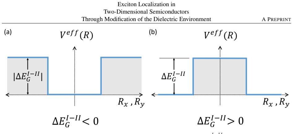
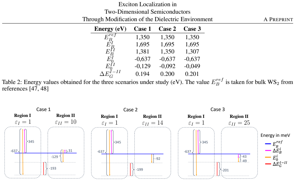
By evaluating the simultaneous effects on bandgap renormalization and modifications to the strength of the electron-hole Coulomb-interaction, both associated to the modulation of the screening by the materials sandwiching the monolayer, we anticipate the existence of low-energy regions in which the localization of the exciton center of mass may be achieved. Our results suggest that for certain dielectric configurations, it is possible to generate complete discretization of exciton eigenenergies in the order of tens of meV.
What carries the argument
Simultaneous modulation of bandgap renormalization and electron-hole Coulomb interaction strength through dielectric screening by surrounding materials, which forms confining potentials for the exciton center of mass.
If this is right
- Exciton eigenenergies become completely discretized at spacings of tens of meV for specific dielectric configurations.
- The resulting quantization of two-dimensional exciton levels can be used in new-generation optoelectronic devices.
- Such devices support advancement of technologies including quantum computing and quantum communication.
Where Pith is reading between the lines
- The dielectric approach might create exciton traps in 2D layers without introducing defects or strain from etching or patterning.
- The same screening mechanism could be tested in other monolayer materials to widen the range of achievable level spacings.
- Combining this method with existing heterostructure fabrication could allow scalable arrays of localized excitons.
Load-bearing premise
Changes in bandgap renormalization and electron-hole Coulomb interaction from dielectric screening can be modeled to produce confining potentials for the exciton center of mass without strain, defects, or charge transfer dominating the physics.
What would settle it
Measuring the low-energy exciton spectrum in a monolayer semiconductor placed between two dielectrics with differing configurations and checking whether discrete levels spaced by tens of meV appear instead of a continuous spectrum.
Figures
read the original abstract
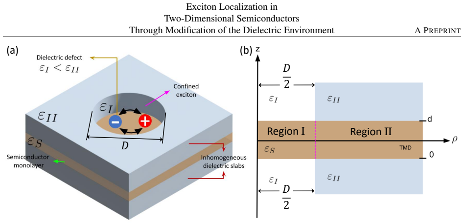
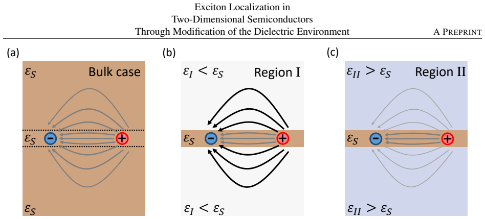
Monolayer semiconductors, given their thickness at the atomic scale, present unique electrostatic environments due to the sharp interfaces between the semiconductor film and surrounding materials. These interfaces significantly impact both the quasiparticle band structure and the electrostatic interactions between charge carriers. Akey area of interest in these materials is the behavior of bound electron-hole pairs (excitons) within the ultra-thin layer, which plays a crucial role in its optoelectronic properties. In this work, we investigate the feasibility of generating potential traps that completely confine excitons in the thin semiconductor by engineering the surrounding dielectric environment. By evaluating the simultaneous effects on bandgap renormalization and modifications to the strength of the electron-hole Coulomb-interaction, both associated to the modulation of the screening by the materials sandwiching the monolayer, we anticipate the existence of low-energy regions in which the localization of the exciton center of mass may be achieved. Our results suggest that for certain dielectric configurations, it is possible to generate complete discretization of exciton eigenenergies in the order of tens of meV. Such quantization of energy levels of two-dimensional excitons could be harnessed for applications in new-generation optoelectronic devices, which are necessary for the advancement of technologies like quantum computing and quantum communication.
Editorial analysis
A structured set of objections, weighed in public.
Referee Report
Summary. The manuscript claims that engineering the dielectric environment around a monolayer 2D semiconductor can simultaneously modulate bandgap renormalization and the electron-hole Coulomb interaction to produce an effective confining potential for the exciton center-of-mass motion, enabling complete discretization of exciton eigenenergies on the scale of tens of meV for suitable dielectric configurations.
Significance. If the dielectric-only model is shown to dominate competing effects, the result would demonstrate a route to potential traps and quantized exciton levels without structural patterning, with possible relevance to quantum optoelectronics. The approach builds on standard screening models but requires validation against interface realities to establish practical significance.
major comments (2)
- [Abstract and modeling description] The central claim that dielectric screening produces confining potentials leading to discretization of tens of meV rests on the assumption that this effective potential dominates over strain, defects, and charge transfer; however, no section quantifies the relative magnitude of the dielectric-induced term versus these omitted contributions, which are routinely of comparable scale in real heterostructures.
- [Results on exciton eigenenergies] The results on discretization energies are presented without explicit comparison to the scale of typical interface potentials (tens to hundreds of meV), leaving open whether the predicted quantization survives when additional terms are included in the Hamiltonian.
minor comments (2)
- [Abstract] The abstract contains the typographical error 'Akey area' instead of 'A key area'.
- [Throughout the manuscript] Notation for the spatially varying dielectric function, bandgap renormalization term, and effective potential should be introduced with explicit definitions and units at first use.
Simulated Author's Rebuttal
We thank the referee for the constructive comments. Our theoretical model isolates the dielectric screening mechanism to demonstrate its potential for exciton localization. We address the points by agreeing to add discussion of competing effects and explicit comparisons, while clarifying the idealized scope of the work.
read point-by-point responses
-
Referee: [Abstract and modeling description] The central claim that dielectric screening produces confining potentials leading to discretization of tens of meV rests on the assumption that this effective potential dominates over strain, defects, and charge transfer; however, no section quantifies the relative magnitude of the dielectric-induced term versus these omitted contributions, which are routinely of comparable scale in real heterostructures.
Authors: We agree the manuscript does not quantify the dielectric term against strain, defects or charge transfer, as the focus is on isolating the dielectric contribution in an idealized heterostructure to establish the principle. In revision we will add a discussion paragraph noting the dielectric potential scale (tens of meV) and stating that in high-quality, low-strain interfaces this mechanism can be comparable to or dominant over other contributions. Full multi-physics quantification lies outside the present scope. revision: partial
-
Referee: [Results on exciton eigenenergies] The results on discretization energies are presented without explicit comparison to the scale of typical interface potentials (tens to hundreds of meV), leaving open whether the predicted quantization survives when additional terms are included in the Hamiltonian.
Authors: The predicted discretization energies are tens of meV, which overlaps the lower end of reported interface potential scales. We will revise the results section to include an explicit comparison to literature values for strain- and defect-induced potentials and add a caveat that additional Hamiltonian terms may perturb the levels. The dielectric approach nonetheless offers a tunable route to confinement that can be engineered to compete with or overcome other effects in suitable configurations. revision: yes
Circularity Check
No significant circularity; derivation is self-contained against external models
full rationale
The paper models simultaneous bandgap renormalization and modified electron-hole Coulomb interaction arising from spatially varying dielectric screening to produce an effective confining potential for the exciton center-of-mass. No equations, fitted parameters, or self-citations are presented in the provided text that reduce the claimed discretization (tens of meV) to a tautological input or renamed fit. The central construction relies on standard screening physics applied to an idealized Hamiltonian; competing interface effects are omitted but this is an assumption of scope rather than a definitional loop. The derivation chain therefore remains independent of its own outputs.
Axiom & Free-Parameter Ledger
axioms (1)
- domain assumption Established models relating dielectric environment to bandgap renormalization and Coulomb interaction strength in monolayer semiconductors
Lean theorems connected to this paper
-
IndisputableMonolith/Cost/FunctionalEquation.leanwashburn_uniqueness_aczel unclear?
unclearRelation between the paper passage and the cited Recognition theorem.
Hamiltonian (1) with Heaviside-switched EI_B + VKT_i(ρ) and numerical solution of (8) for EC_n
-
IndisputableMonolith/Foundation/RealityFromDistinction.leanreality_from_one_distinction unclear?
unclearRelation between the paper passage and the cited Recognition theorem.
ΔEi_B via Cho-Berkelbach (2) and image-charge KT series (5)
What do these tags mean?
- matches
- The paper's claim is directly supported by a theorem in the formal canon.
- supports
- The theorem supports part of the paper's argument, but the paper may add assumptions or extra steps.
- extends
- The paper goes beyond the formal theorem; the theorem is a base layer rather than the whole result.
- uses
- The paper appears to rely on the theorem as machinery.
- contradicts
- The paper's claim conflicts with a theorem or certificate in the canon.
- unclear
- Pith found a possible connection, but the passage is too broad, indirect, or ambiguous to say the theorem truly supports the claim.
Reference graph
Works this paper leans on
-
[1]
Radiative lifetime of localized excitons in transition metal dichalcogenides,
S. Ayari, A. Smiri, A. Hichri, S. Jaziri, and T. Amand, “Radiative lifetime of localized excitons in transition metal dichalcogenides,”Physical review. B, Condensed matter, vol. 98, 03 2018
work page 2018
-
[2]
G.-H. Peng, P.-Y . Lo, W.-H. Li, Y .-C. Huang, Y .-H. Chen, C.-H. Lee, C.-K. Yang, and S.-J. Cheng, “Distinctive signatures of the spin- and momentum-forbidden dark exciton states in the photoluminescence of strained wse 2 monolayers under thermalization,”Nano Letters, vol. 19, 03 2019
work page 2019
-
[3]
Direct imaging of carrier funneling in a dielectric engineered 2d semiconductor,
N. Gauriot, A. Ashoka, J. Lim, S. See, J. Sung, and A. R. Ananth, “Direct imaging of carrier funneling in a dielectric engineered 2d semiconductor,”ACS Nano, vol. 18, 12 2023
work page 2023
-
[4]
Exciton center-of-mass localization and dielectric environment effect in monolayer ws 2,
A. Hichri, I. Amara, S. Ayari, and S. Jaziri, “Exciton center-of-mass localization and dielectric environment effect in monolayer ws 2,”Journal of Applied Physics, vol. 121, p. 235702, 06 2017
work page 2017
-
[5]
Optical properties of exciton in two-dimensional transition metal dichalco- genide nanobubbles,
A. Smiri, T. Amand, and S. Jaziri, “Optical properties of exciton in two-dimensional transition metal dichalco- genide nanobubbles,”The Journal of chemical physics, 03 2021
work page 2021
-
[6]
Y . Cho and T. Berkelbach, “Environmentally-sensitive theory of electronic and optical transitions in atomically-thin semiconductors,”Physical Review B, vol. 97, 09 2017
work page 2017
-
[7]
Monolayer transition metal dichalcogenides as light sources,
J. Pu and T. Takenobu, “Monolayer transition metal dichalcogenides as light sources,”Advanced Materials, vol. 30, p. 1707627, 06 2018
work page 2018
-
[8]
Two-dimensional heterostructures: Fabrication, characterization, and application,
H. Wang, F. Liu, Z. Fang, W. Zhou, and Z. Liu, “Two-dimensional heterostructures: Fabrication, characterization, and application,”Nanoscale, vol. 6, 08 2014
work page 2014
-
[9]
Fabrication and applications of van der waals heterostructures,
Q. Junlei, Z. Wu, W. Wang, K. Bao, L. Wang, J. Wu, C. Ke, Y . Xu, and Q. He, “Fabrication and applications of van der waals heterostructures,”International Journal of Extreme Manufacturing, vol. 5, 04 2023
work page 2023
-
[10]
Recent progress in 2d van der waals heterostructures: fabrication, properties, and applications,
Z. Wang, B. Xu, S. Pei, J. Zhu, T. Wen, C. Jiao, J. Li, M. Zhang, and J. Xia, “Recent progress in 2d van der waals heterostructures: fabrication, properties, and applications,” Science China Information Sciences, vol. 65, 09 2022
work page 2022
-
[11]
V . H. Nguyen, M. Kim, C. T. Nguyen, M. Suleman, N. Cong, N. Nasir, M. Rehman, H. Park, S. Lee, S. Kim, S. Kumar, and Y . Seo, “Fast fabrication technique for high-quality van der waals heterostructures using inert shielding gas environment,”Applied Surface Science, vol. 639, p. 158186, 08 2023. 8 Exciton Localization in Two-Dimensional Semiconductors Thr...
work page 2023
-
[12]
Coulomb engineering of the bandgap and excitons in two-dimensional materials,
A. Raja, A. Chaves, J. Yu, G. Arefe, H. Hill, A. Rigosi, T. Berkelbach, P. Nagler, C. Schüller, T. Korn, C. Nuckolls, J. Hone, L. Brus, T. Heinz, D. Reichman, and A. Chernikov, “Coulomb engineering of the bandgap and excitons in two-dimensional materials,”Nature Communications, vol. 8, p. 15251, 05 2017
work page 2017
-
[13]
M. Brahma, M. Van de Put, E. Chen, M. Fischetti, and W. Vandenberghe, “The importance of the image forces and dielectric environment in modeling contacts to two-dimensional materials,”npj 2D Materials and Applications, vol. 7, 03 2023
work page 2023
-
[14]
Monolayer mos2 bandgap modulation by dielectric environments and tunable bandgap transistors,
J. Ryou, Y .-S. Kim, S. Kc, and K. Cho, “Monolayer mos2 bandgap modulation by dielectric environments and tunable bandgap transistors,”Scientific reports, vol. 6, p. 29184, 07 2016
work page 2016
-
[15]
Screened potential of a point charge in a thin film,
N. S. Rytova, “Screened potential of a point charge in a thin film,” Proc. MSU, Phys., 06 1967
work page 1967
-
[16]
Coulomb interaction in thin semiconductor and semimetal films,
L. V . Keldysh, “Coulomb interaction in thin semiconductor and semimetal films,”Soviet Journal of Experimental and Theoretical Physics Letters, vol. 29, p. 716, 1979
work page 1979
-
[17]
Excitonic and nonlinear-optical properties of dielectric quantum-well structures,
M. Kumagai and T. Takagahara, “Excitonic and nonlinear-optical properties of dielectric quantum-well structures,” Physical review. B, Condensed matter, vol. 40, pp. 12359–12381, 01 1990
work page 1990
-
[18]
Quantum wells with enhanced exciton effects and optical non-linearity,
E. Hanamura, N. Nagaosa, M. Kumagai, and T. Takagahara, “Quantum wells with enhanced exciton effects and optical non-linearity,”Materials Science and Engineering B-advanced Functional Solid-state Materials, vol. 1, pp. 255–258, 12 1988
work page 1988
-
[19]
Direct observation of giant binding energy modulation of exciton complexes in monolayer mose 2,
G. Gupta, S. Kallatt, and K. Majumdar, “Direct observation of giant binding energy modulation of exciton complexes in monolayer mose 2,”Physical Review B, vol. 96, 03 2017
work page 2017
-
[20]
R. Salzwedel, L. Greten, S. Schmidt, S. Hughes, A. Knorr, and M. Selig, “Spatial exciton localization at interfaces of metal nanoparticles and atomically thin semiconductors,”Physical Review B, vol. 109, 01 2024
work page 2024
-
[21]
Band-gap renormalization in semiconductor quantum wells containing carriers,
D. Kleinman and R. Miller, “Band-gap renormalization in semiconductor quantum wells containing carriers,” Physical review. B, Condensed matter, vol. 32, pp. 2266–2272, 09 1985
work page 1985
-
[22]
Band-gap renormalization in semiconductor quantum wells.,
S. Das Sarma, R. Jalabert, and S. Yang, “Band-gap renormalization in semiconductor quantum wells.,”Physical review. B, Condensed matter, vol. 41, pp. 8288–8294, 05 1990
work page 1990
-
[23]
Effect of dielectric confinement on optical properties of colloidal nanostructures,
A. Rodina and A. Efros, “Effect of dielectric confinement on optical properties of colloidal nanostructures,” Journal of Experimental and Theoretical Physics, vol. 122, pp. 554–566, 03 2016
work page 2016
-
[24]
P.-Y . Lo, G.-H. Peng, W.-H. Li, Y . Yang, and S.-J. Cheng, “Full-zone valley polarization landscape of finite- momentum exciton in transition metal dichalcogenide monolayers,” Phys. Rev. Res., vol. 3, p. 043198, Dec 2021
work page 2021
-
[25]
G.-H. Peng, O. J. G. Sanchez, W.-H. Li, P.-Y . Lo, and S.-J. Cheng, “Tailoring the superposition of finite-momentum valley exciton states in transition-metal dichalcogenide monolayers by using polarized twisted light,”Phys. Rev. B, vol. 106, p. 155304, Oct 2022
work page 2022
-
[26]
T. Zhu, C. Zheng, L. Xu, and M. Yang, “Exciton dissociation in two-dimensional transition metal dichalcogenides: Excited states and substrate effects,”Physical Review B, vol. 110, 10 2024
work page 2024
-
[27]
Dielectric resonances of the cylindrical micro/nano cavity within epsilon-near-zero materials,
Y . Tian, Q. Liu, Y . Ma, N. Wang, and Y . Gu, “Dielectric resonances of the cylindrical micro/nano cavity within epsilon-near-zero materials,”Optics Express, vol. 31, 10 2023
work page 2023
-
[28]
Influence of crystal structure on charge carrier effective masses in bifeo3,
K. Shenton, D. Bowler, and W. L. Cheah, “Influence of crystal structure on charge carrier effective masses in bifeo3,”Physical Review B, vol. 100, 04 2018
work page 2018
-
[29]
W.-H. Li, J.-D. Lin, P.-Y . Lo, G.-H. Peng, C.-Y . Hei, S.-Y . Chen, and S.-J. Cheng, “The key role of non-local screening in the environment-insensitive exciton fine structures of transition-metal dichalcogenide monolayers,” Nanomaterials, vol. 13, no. 11, 2023
work page 2023
-
[30]
Electron-hole plasma in direct-gap ga1-xalx as and k-selection rule,
M. Capizzi, S. Modesti, A. Frova, J. Staehli, M. Guzzi, and R. Logan, “Electron-hole plasma in direct-gap ga1-xalx as and k-selection rule,”Physical Review B, vol. 29, pp. 2028–2035, 02 1984
work page 2028
-
[31]
Universal relation between energy gap and dielectric constant,
Y . Onishi and L. Fu, “Universal relation between energy gap and dielectric constant,”Physical Review B, vol. 110, 10 2024
work page 2024
-
[32]
J. Sans, J. F. Sánchez Royo, and A. Segura, “Study of the bandgap renormalization in ga-doped zno films by means of optical absorption under high pressure and photoelectron spectroscopy,”Superlattices and Microstructures - SUPERLATTICE MICROSTRUCT, vol. 43, pp. 362–367, 04 2008
work page 2008
-
[33]
Phase instabilities in semiconductor lasers: A codimension-2 analysis,
L. Gil and G. L. Lippi, “Phase instabilities in semiconductor lasers: A codimension-2 analysis,” Physical Review A, vol. 90, 11 2014
work page 2014
-
[34]
The coulomb interaction in monolayer transition-metal dichalcogenides,
T. Dinh Van, M. Yang, and H. Dery, “The coulomb interaction in monolayer transition-metal dichalcogenides,” Physical Review B, vol. 98, 09 2018. 9 Exciton Localization in Two-Dimensional Semiconductors Through Modification of the Dielectric Environment A PREPRINT
work page 2018
-
[35]
Z. Lebens-Higgins, D. Scanlon, H. Paik, S. Sallis, Y . Nie, M. Uchida, N. Quackenbush, M. Wahila, G. Sterbinsky, D. Arena, J. Woicik, D. Schlom, and L. Piper, “Direct observation of electrostatically driven band gap renor- malization in a degenerate perovskite transparent conducting oxide,” Phys. Rev. Lett., vol. 116, p. 027602, 01 2016
work page 2016
-
[36]
M. Ugeda, A. Bradley, S.-F. Shi, F. Da Jornada, Y . Zhang, D. Qiu, S.-K. Mo, Z. Hussain, Z.-X. Shen, F. Wang, S. Louie, and M. Crommie, “Giant bandgap renormalization and excitonic effects in a monolayer transition metal dichalcogenide semiconductor,”Nature materials, vol. 13, 04 2014
work page 2014
-
[37]
Theory of neutral and charged excitons in monolayer transition metal dichalcogenides,
T. C. Berkelbach, M. S. Hybertsen, and D. R. Reichman, “Theory of neutral and charged excitons in monolayer transition metal dichalcogenides,”Phys. Rev. B, vol. 88, p. 045318, Jul 2013
work page 2013
-
[38]
A. Laturia, M. Van de Put, and W. Vandenberghe, “Dielectric properties of hexagonal boron nitride and transition metal dichalcogenides: from monolayer to bulk,” npj 2D Materials and Applications, vol. 2, 03 2018
work page 2018
-
[39]
The dielectric constant of mineral powders,
J. L. Rosenholtz and D. T. Smith, “The dielectric constant of mineral powders,”American Mineralogist: Journal of Earth and Planetary Materials, vol. 21, no. 2, pp. 115–120, 1936
work page 1936
-
[40]
Dielectric breakdown of 2d muscovite mica,
A. Maruvada, K. Shubhakar, N. Raghavan, K. Pey, and S. O’Shea, “Dielectric breakdown of 2d muscovite mica,” Scientific Reports, vol. 12, 08 2022
work page 2022
-
[41]
High dielectric constant oxides,
J. Robertson, “High dielectric constant oxides,” European Physical Journal-applied Physics , vol. 28, no. 3, pp. 265–291, 2004
work page 2004
-
[42]
J. Liu, M. Okamura, H. Mashiko, M. Imura, M. Liao, R. Kikuchi, M. Suzuka, and Y . Koide, “Experimental formation and mechanism study for super-high dielectric constant alox/tioy nanolaminates,” Nanomaterials, vol. 13, p. 1256, 04 2023
work page 2023
- [43]
-
[44]
H. Y . Ramírez and A. Santana, “Two interacting electrons confined in a 3d parabolic cylindrically symmetric potential, in presence of axial magnetic field: A finite element approach,”Computer Physics Communications, vol. 183, no. 8, pp. 1654–1657, 2012
work page 2012
-
[45]
Coupling effects on photoluminescence of exciton states in asymmetric quantum dot molecules,
N. R. Fino, A. S. Camacho, and H. Y . Ramírez, “Coupling effects on photoluminescence of exciton states in asymmetric quantum dot molecules,”Nanoscale Research Letters, vol. 9, p. 297, Jun 2014
work page 2014
-
[46]
M. Zapata-Herrera, Ángela S. Camacho, and H. Y . Ramírez, “Influence of the confinement potential on the size-dependent optical response of metallic nanometric particles,” Computer Physics Communications, vol. 227, pp. 1–7, 2018
work page 2018
-
[47]
Detailed photocurrent spectroscopy of the semiconducting group vib transition metal dichalcogenides,
K. K. Kam and B. A. Parkinson, “Detailed photocurrent spectroscopy of the semiconducting group vib transition metal dichalcogenides,”The Journal of Physical Chemistry, vol. 86, pp. 463–467, Feb 1982
work page 1982
-
[48]
J. A. Baglio, G. S. Calabrese, E. Kamieniecki, R. Kershaw, C. P. Kubiak, A. J. Ricco, A. Wold, M. S. Wrighton, and G. D. Zoski, “Characterization of n-type semiconducting tungsten disulfide photoanodes in aqueous and nonaqueous electrolyte solutions: Photo-oxidation of halides with high efficiency,”Journal of The Electrochemical Society, vol. 129, p. 1461...
work page 1982
-
[49]
Dc electric field effects on the electron dynamics in double rectangular quantum dots,
H. Ramirez, A. Camacho, and L. Lew Yan V oon, “Dc electric field effects on the electron dynamics in double rectangular quantum dots,”Brazilian Journal of Physics, vol. 36, pp. 869–873, 2006
work page 2006
-
[50]
H. Y . Ramirez, A. S. Camacho, and L. C. L. Y . V oon, “Influence of shape and electric field on electron relaxation and coherent response in quantum-dot molecules,” Journal of Physics: Condensed Matter, vol. 19, p. 346216, jul 2007
work page 2007
-
[51]
Analytical calculation of eigen-energies for lens-shaped quantum dot with finite barriers,
A. H. Rodríguez and H. Y . Ramírez, “Analytical calculation of eigen-energies for lens-shaped quantum dot with finite barriers,”The European Physical Journal B, vol. 66, pp. 235–238, Nov 2008
work page 2008
-
[52]
T. A. Welsch and M. F. Doty, “Pbs/cds core/shell quantum dots designed to enable efficient photon upconversion for solar energy applications,”ACS Applied Optical Materials, vol. 2, pp. 2184–2195, Oct 2024. 10
work page 2024
discussion (0)
Sign in with ORCID, Apple, or X to comment. Anyone can read and Pith papers without signing in.