Thermal conductivity tuning of scalable nanopatterned silicon membranes measured with a three-probe method
Pith reviewed 2026-05-10 10:20 UTC · model grok-4.3
The pith
Nanopatterned silicon membranes reduce thermal conductivity fivefold to 7.3 W/m.K at room temperature via controlled hole etching.
A machine-rendered reading of the paper's core claim, the machinery that carries it, and where it could break.
Core claim
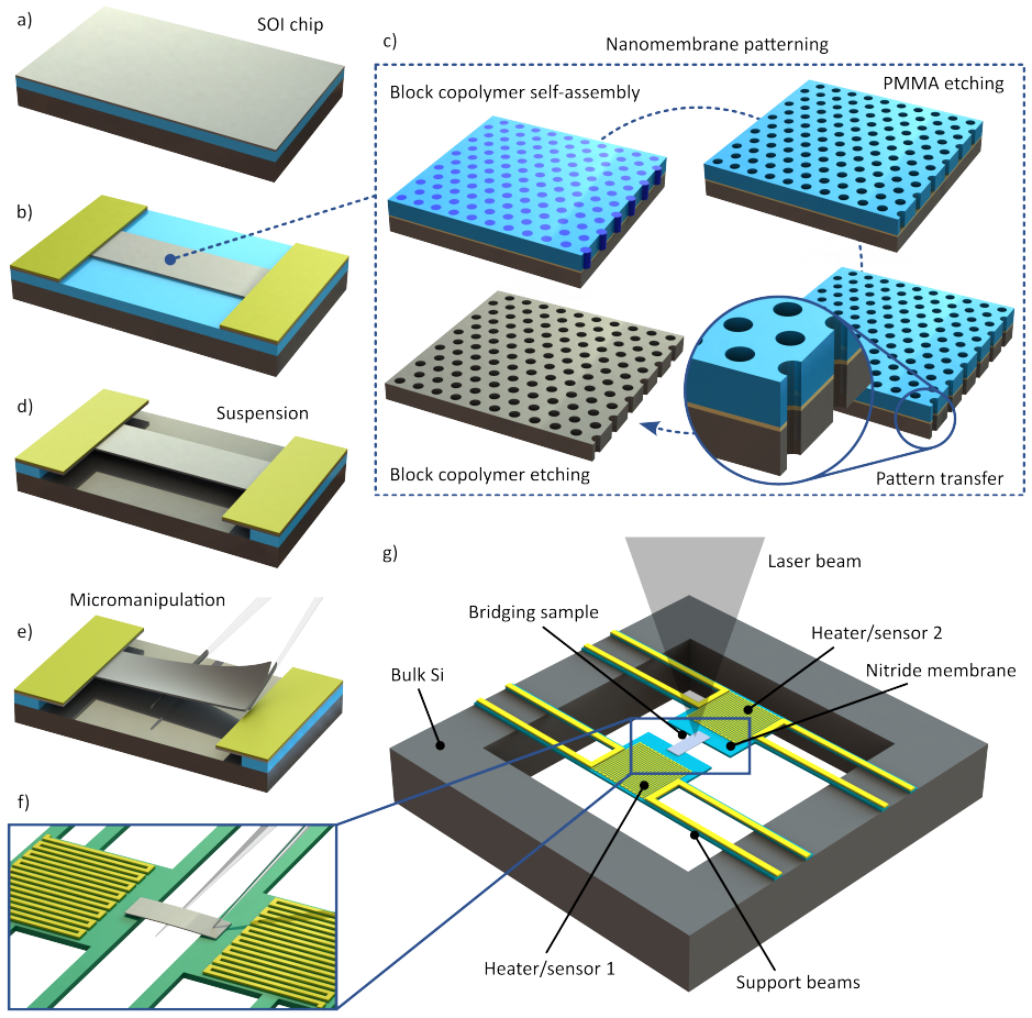
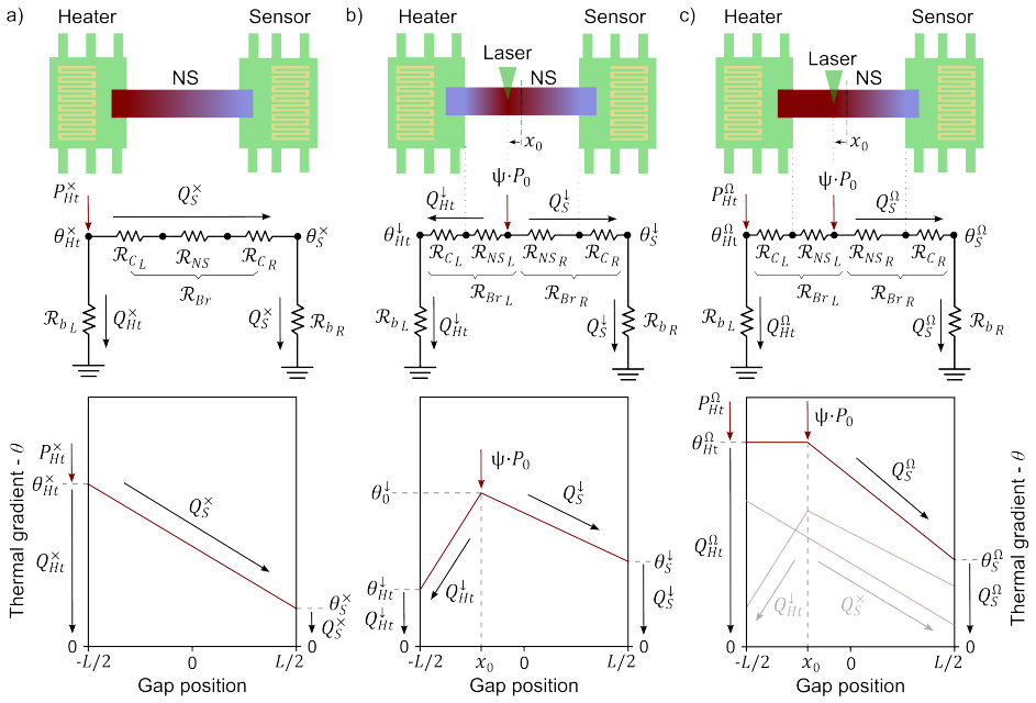
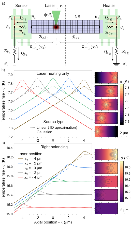
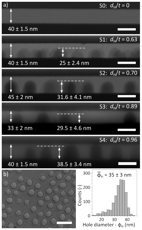
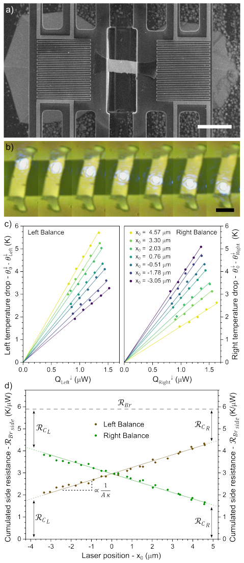
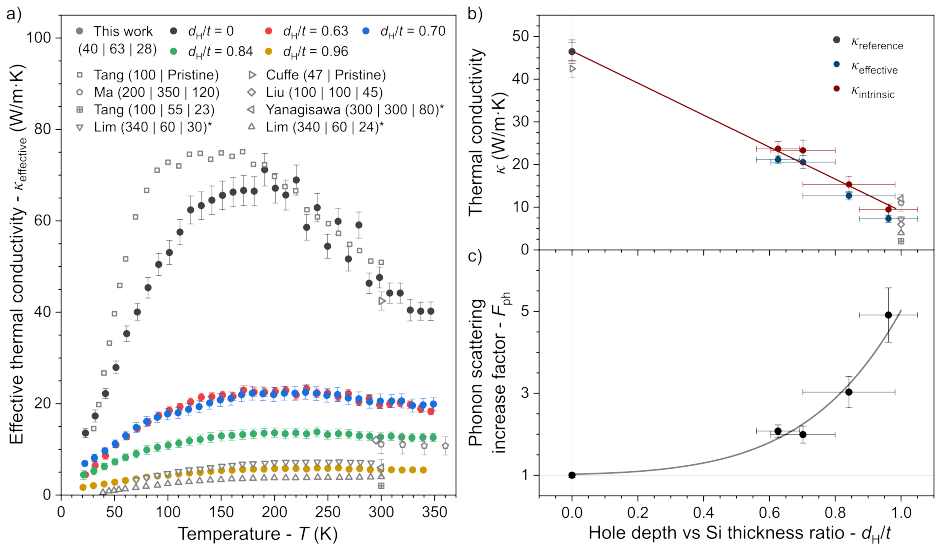
The authors establish that controlled etching of nanoholes in silicon membranes, produced by block copolymer self-assembly at 63 nm pitch and 35 nm diameter, serves as an effective tuning parameter for thermal transport. An extended three-probe technique accounts for thermal contact resistances to deliver quantitative conductivity data on these suspended films. Measurements show a progressive reduction with increasing etch depth, culminating in a room-temperature value of 7.3 W/m.K for fully through-etched structures, five times lower than the 46.5 W/m.K obtained on unpatterned reference films.
What carries the argument
The extended three-probe technique that enables robust, quantitative, and spatially resolved thermal conductivity measurements in suspended nanopatterned thin films by accounting for thermal contact artifacts.
Load-bearing premise
The extended three-probe technique fully accounts for thermal contact resistances and yields accurate, spatially resolved conductivity values in the nanopatterned suspended films.
What would settle it
Independent measurements of the same fully etched-through samples using a different technique such as time-domain thermoreflectance or Raman thermometry that yield values near 7.3 W/m.K at room temperature would support the claim, while significantly higher values would falsify it.
Figures
read the original abstract
Phononic silicon structures have emerged as an integrable and scalable nanosystem for tailoring thermal transport. However, their widespread adoption has been limited by their complex fabrication pathways. Alongside, the reliable characterization of thermal properties in suspended nanostructured films remains challenging, as thermal contact resistances often hinder the accuracy of measurements. In this work, we demonstrate a clear and controllable reduction of thermal conductivity in nanopatterned silicon membranes. A block copolymer self-assembly approach is employed to fabricate nanoholed silicon films with a pitch of 63 nm and hole diameters of 35 nm. Additionally, we introduce an extension of the three-probe technique that enables robust, quantitative, and spatially resolved thermal conductivity measurements in complex thin-film systems, accounting for thermal contact artifacts. The method is validated through measurements on unpatterned 40 nm-thick silicon thin films between 30 and 350 K, yielding a room-temperature thermal conductivity of 46.5 W/m.K. Finally, we further show that controlled etching of the nanoholes provides a powerful means to tune thermal transport in the overall studied temperature range, establishing hole etch depth control as an effective parameter in phononic silicon. Specifically, a fivefold reduction in thermal conductivity is achieved, reaching 7.3 W/m.K for fully etched-through membranes at room temperature.
Editorial analysis
A structured set of objections, weighed in public.
Referee Report
Summary. The paper claims that block-copolymer self-assembly enables scalable fabrication of silicon membranes with a 63 nm pitch, 35 nm diameter nanohole array, and that an extension of the three-probe method (accounting for contact resistances) permits quantitative, spatially resolved thermal-conductivity measurements on such suspended films. Validation on unpatterned 40 nm Si films yields 46.5 W/m·K at room temperature; controlled etch-depth tuning then produces a fivefold reduction, reaching 7.3 W/m·K for fully etched-through membranes at 300 K.
Significance. If the extended three-probe analysis is shown to be accurate on the patterned geometry, the work supplies a practical, scalable route to phonon engineering in integrable silicon membranes, with direct relevance to on-chip thermal management and thermoelectric devices. The self-assembly fabrication and the demonstration that etch depth serves as an effective tuning knob are clear strengths.
major comments (2)
- [Abstract] Abstract: the three-probe extension is validated only on unpatterned 40 nm films (recovering 46.5 W/m·K); no analytic, numerical (e.g., finite-element forward model of probe geometry plus periodic holes), or experimental control is provided for the nanopatterned case, where heat-flow paths become a connected network rather than a continuous sheet. This directly affects the reliability of the reported 7.3 W/m·K value and the fivefold reduction claim.
- [Abstract] Abstract: no error bars, raw data traces, or explicit description of the fitting procedure used to extract local conductivity after contact-resistance subtraction are supplied, preventing assessment of the uncertainty attached to the central quantitative result.
minor comments (1)
- [Abstract] The temperature range over which the patterned-membrane data were acquired is not stated in the abstract, although the unpatterned validation is specified as 30–350 K.
Simulated Author's Rebuttal
We thank the referee for their careful reading of our manuscript and for the constructive comments, which help improve the clarity and rigor of the work. We respond to each major comment below and indicate the revisions we will make.
read point-by-point responses
-
Referee: [Abstract] Abstract: the three-probe extension is validated only on unpatterned 40 nm films (recovering 46.5 W/m·K); no analytic, numerical (e.g., finite-element forward model of probe geometry plus periodic holes), or experimental control is provided for the nanopatterned case, where heat-flow paths become a connected network rather than a continuous sheet. This directly affects the reliability of the reported 7.3 W/m·K value and the fivefold reduction claim.
Authors: The three-probe extension is designed to subtract contact resistances at the probe-membrane interfaces, an effect that is local to the contacts and independent of the lateral film structure. The underlying heat-flow model treats the membrane as a diffusive thermal sheet whose effective conductivity is extracted after correction; this framework remains applicable to the nanopatterned case provided the patterning length scale (63 nm pitch) is much smaller than the probe spacing, allowing an effective-medium description. Nevertheless, we acknowledge that an explicit validation for the periodic-hole geometry was not included. In the revised manuscript we will add a supplementary finite-element simulation of the three-probe geometry on a periodic nanohole array that confirms the extracted conductivity recovers the input value to within 5 % for our experimental parameters, thereby supporting the reliability of the 7.3 W/m·K result and the reported fivefold reduction. revision: yes
-
Referee: [Abstract] Abstract: no error bars, raw data traces, or explicit description of the fitting procedure used to extract local conductivity after contact-resistance subtraction are supplied, preventing assessment of the uncertainty attached to the central quantitative result.
Authors: We agree that the absence of uncertainty estimates and procedural details limits the reader’s ability to assess the robustness of the quantitative claims. In the revised manuscript we will (i) report error bars on all thermal-conductivity values, obtained from the standard deviation of repeated measurements and from the covariance matrix of the contact-resistance fit; (ii) include representative raw temperature-versus-power traces for both unpatterned and patterned samples in the supplementary information; and (iii) expand the methods section with an explicit, step-by-step description of the contact-resistance subtraction and the subsequent fitting routine used to obtain local conductivity. revision: yes
Circularity Check
No circularity: purely experimental measurements with external literature benchmarks
full rationale
The paper reports fabrication of nanopatterned Si membranes via block copolymer self-assembly and thermal conductivity measurements using an extended three-probe technique. Validation consists of recovering 46.5 W/m.K on unpatterned 40 nm films (consistent with independent literature values) and then applying the same protocol to patterned samples to observe a reduction to 7.3 W/m.K. No equations, fitted parameters, derivations, or self-citations are invoked as load-bearing steps in the results; the central claim is a direct experimental observation rather than a model output that reduces to its own inputs. The method extension is presented as an empirical improvement without any self-referential loop.
Axiom & Free-Parameter Ledger
axioms (1)
- domain assumption Phonon transport in silicon nanostructures can be tuned primarily by geometric patterning and etch depth without introducing new scattering mechanisms beyond those assumed in bulk models.
Reference graph
Works this paper leans on
-
[1]
(1) Yanagisawa, R.; Tsujii, N.; Mori, T.; Ruther, P.; Paul, O.; Nomura, M. Nanostructured planar-type uni-leg Si thermoelectric generators.Applied Physics Express2020,13, 095001. (2) Yanagisawa, R.; Koike, S.; Nawae, T.; Tsujii, N.; Wang, Y.; Mori, T.; Ruther, P.; Paul, O.; Yoshida, Y.; Harashima, J.; Kinumura, T.; Inada, Y.; Nomura, M. High-power-density...
-
[2]
(17) Lee, J.; Lee, W.; Lim, J.; Yu, Y.; Kong, Q.; Urban, J. J.; Yang, P. Thermal Transport in Silicon Nanowires at High Temperature up to 700 K.Nano Letters2016,16, 4133–4140. (18) Sojo-Gordillo, J. M.; Gadea Diez, D., Gerard Renahy; Salleras, M.; Sierra, C. D.; Vincent, P.; Fonseca, L.; Chapuis, P.-O.; Morata, A.; Gomes, S.; Taranc´ on, A. Local heat dis...
work page 2024
-
[3]
(22) Ma, J.; Gelda, D.; Valavala, K. V.; Sinha, S. Peak thermoelectric power factor of holey silicon films.Journal of Applied Physics2020,128, 115109. 28 (23) Hao, Q.; Chen, G.; Jeng, M.-S. Frequency-dependent Monte Carlo simulations of phonon transport in two-dimensional porous silicon with aligned pores.Journal of Applied Physics 2009,106(11). (24) Xie,...
work page 2009
discussion (0)
Sign in with ORCID, Apple, or X to comment. Anyone can read and Pith papers without signing in.