Probing the Valley-Selective Tunneling Density of States in Monolayer MoS2 based Resonant Tunneling Devices
Pith reviewed 2026-05-08 18:29 UTC · model grok-4.3
The pith
Monolayer MoS2 resonant tunneling devices exhibit multiple valley-selective peaks and peak-to-valley ratios of 178 at 4 K and 24 at room temperature.
A machine-rendered reading of the paper's core claim, the machinery that carries it, and where it could break.
Core claim
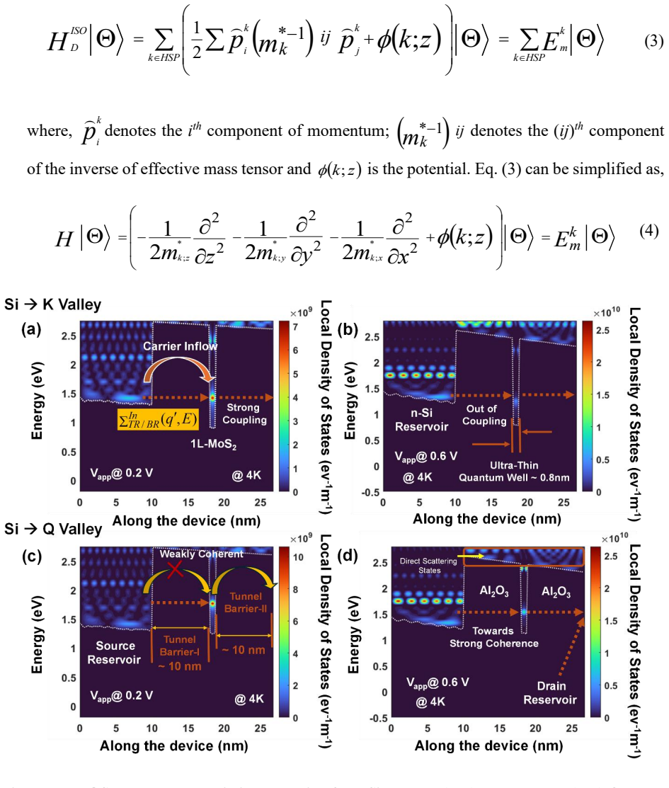
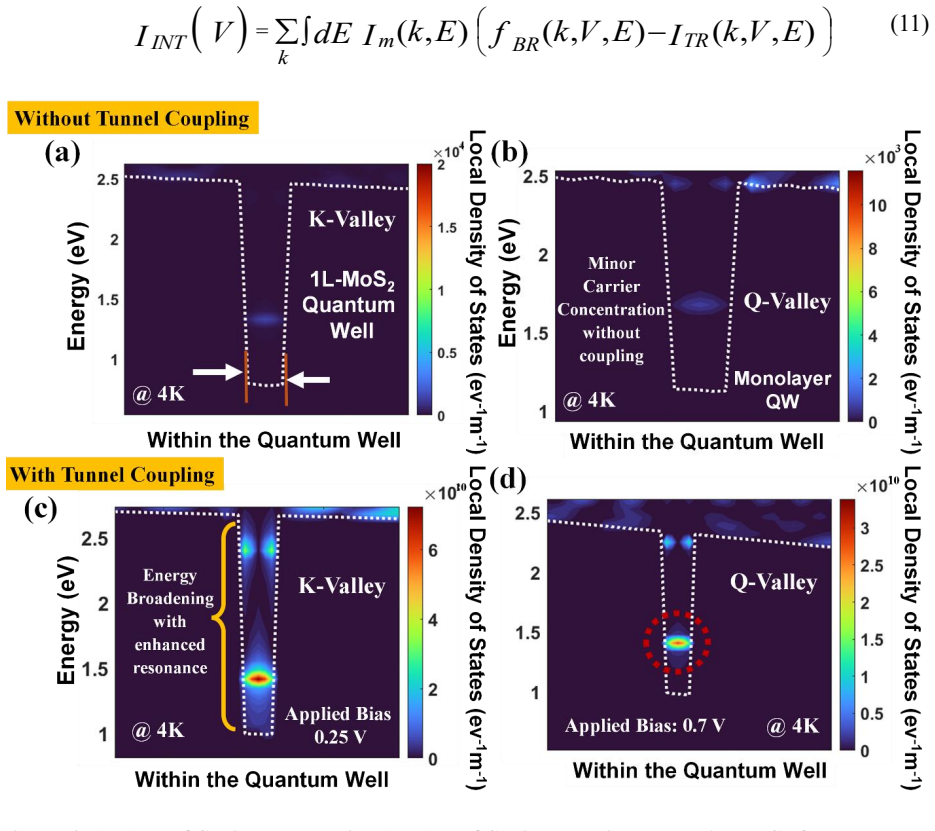
The strongly quantized electronic states from multiple valleys in the momentum space of an ultra-thin monolayer MoS2 sheet, when placed between Al2O3 tunneling barriers, give rise to multiple resonant tunneling peaks. Momentum-conserved and non-conserved tunneling from highly n-doped silicon through these valleys widens the negative-differential-resistance region, a result obtained both from experiment and from density-functional-theory plus non-equilibrium Green-function calculations of the tunneling density of states. The fabricated devices reach peak-to-valley ratios of 178 at 4 K and 24 at room temperature while remaining compatible with conventional CMOS processing.
What carries the argument
Valley-selective tunneling density of states (TDOS) obtained from combined DFT and NEGF modeling, which maps the multiple resonant peaks seen in the experimental I-V curves to distinct valleys of the monolayer MoS2.
Load-bearing premise
The multiple resonant peaks arise from momentum-conserved and non-conserved tunneling through distinct valleys of the monolayer MoS2 rather than from defects, interface states, or other non-valley mechanisms.
What would settle it
If the energies and temperature dependence of the observed peaks match calculated defect or interface levels instead of the valley minima predicted by DFT, or if the peaks remain unchanged when the MoS2 is replaced by a material lacking equivalent valleys, the valley-selective interpretation would be ruled out.
Figures
read the original abstract
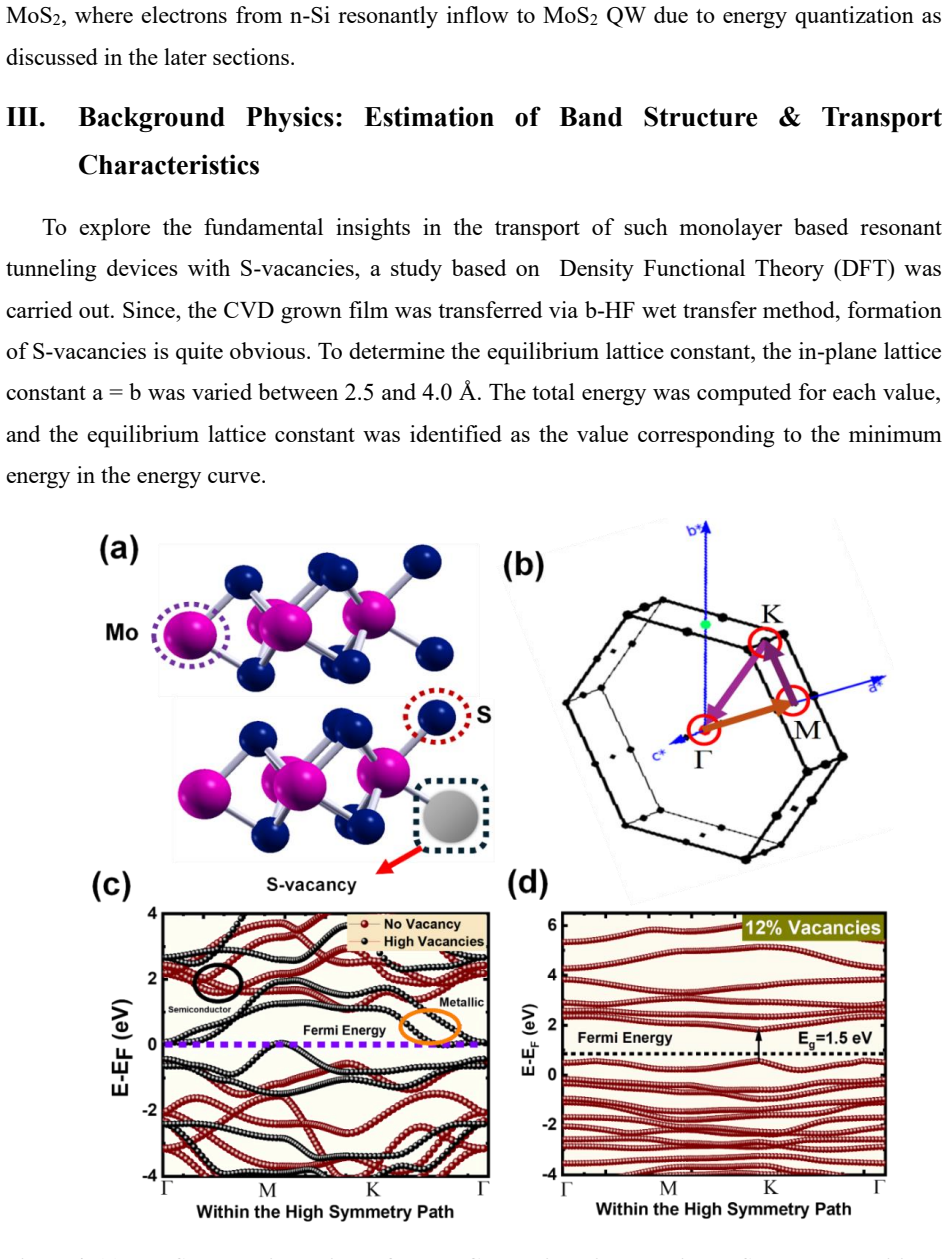
The present work experimentally demonstrates the fabrication of CVD grown monolayer MoS2 ultra thin quantum well based double barrier resonant tunneling device (RTD) architecture well compatible with conventional CMOS fabrication technology. The strongly quantized electronic states from multiple valleys in the momentum space in such ultra 2D sheet along the c-axis sandwiched in between Al2O3 tunneling barriers exhibit multiple resonant tunneling peaks thereby enhancing the FWHM of the NDR region as derived from experimental I-V characteristics as well as theoretical joint invision through Density Functional Theory (DFT) and Non-Equilibrium Greens function (NEGF) visualized via Tunneling Density of States (TDOS). Understanding extended to S-vacancies not only change the bandgap, as evaluated through nanoscale Cathodoluminescence (CL) spectroscopy, but also alters the effective mass hence the mobility as investigated here within the high symmetry path in the k-space. Electrical performances of fabricated RTD, starting from cryogenic to room temperatures, show a significant milestone via exhibiting huge PVR values of 178 at 4K and 24 at RT with more possible improvement in the field of room temperature quantum technology. Momentum conserved and non conserved tunneling from highly n-doped Si through multiple valleys of 1L-MoS2 provides a tremendous opportunity in gate-induced manipulation in Spin-Valley Qubit technology operational at deep cryogenic temperatures (mK).
Editorial analysis
A structured set of objections, weighed in public.
Referee Report
Summary. The manuscript reports fabrication of a double-barrier resonant tunneling device using CVD-grown monolayer MoS2 as the quantum well between Al2O3 barriers on n-doped Si. Experimental I-V curves from 4 K to room temperature show multiple NDR peaks attributed to momentum-conserved and non-conserved tunneling through distinct MoS2 valleys (K, Q, etc.), yielding PVR values of 178 at 4 K and 24 at RT. Supporting data include CL spectroscopy on S-vacancy effects on bandgap and effective mass, plus DFT/NEGF calculations of tunneling density of states (TDOS). The work claims compatibility with CMOS and potential for spin-valley qubits.
Significance. If the NDR peaks can be rigorously shown to originate from valley-selective tunneling, the high PVR values at room temperature would constitute a notable experimental advance for 2D-material-based quantum devices and valleytronics. The multi-technique approach (I-V, CL, DFT/NEGF) is a strength, and the reported PVR numbers exceed many prior 2D RTD reports. However, without controls or quantitative model-experiment matching, the significance remains provisional.
major comments (3)
- [Experimental results / I-V characteristics] Experimental I-V results and discussion: The central claim that multiple resonant peaks arise from valley-selective (momentum-conserved/non-conserved) tunneling through MoS2 valleys lacks control devices (e.g., no-MoS2 barriers, bilayer MoS2, or varied doping) or additional probes (gate or magnetic field dependence) to exclude defect states, S-vacancies, or barrier inhomogeneities as the origin of the NDR features.
- [Theoretical modeling / TDOS] DFT/NEGF TDOS modeling: The calculations assume an ideal monolayer with perfect interfaces, yet the manuscript reports S-vacancies via CL that alter bandgap and effective mass; no quantitative overlay of calculated TDOS peak positions/widths onto experimental NDR voltages, no error bars on data, and no sensitivity analysis to vacancies or interface quality are provided.
- [Electrical characterization] PVR extraction and reproducibility: The headline PVR values (178 at 4 K, 24 at RT) are presented without raw I-V traces, fitting procedures, device-to-device statistics, or yield information, preventing verification that the reported ratios reflect valley physics rather than measurement artifacts or selected devices.
minor comments (3)
- [Abstract] The abstract and text use 'huge PVR' without a quantitative baseline comparison to prior MoS2 or 2D RTD literature.
- [Introduction / Discussion] Valley labels (K, Q, etc.) and the distinction between conserved/non-conserved processes should be defined with a figure or explicit k-space diagram in the main text.
- [Figures] Figure captions for I-V and CL data should specify exact temperature, bias sweep rate, and number of devices measured.
Simulated Author's Rebuttal
We thank the referee for the constructive and detailed comments, which have helped us improve the manuscript. We address each major comment point by point below, providing clarifications based on existing data and making revisions where they strengthen the presentation of valley-selective tunneling without misrepresenting our results.
read point-by-point responses
-
Referee: Experimental I-V results and discussion: The central claim that multiple resonant peaks arise from valley-selective (momentum-conserved/non-conserved) tunneling through MoS2 valleys lacks control devices (e.g., no-MoS2 barriers, bilayer MoS2, or varied doping) or additional probes (gate or magnetic field dependence) to exclude defect states, S-vacancies, or barrier inhomogeneities as the origin of the NDR features.
Authors: We acknowledge that dedicated control devices such as no-MoS2 or bilayer structures would provide additional exclusion of alternative mechanisms. However, the multiple NDR peaks occur at bias voltages that quantitatively align with the distinct K and Q valley energies from our DFT calculations, and their temperature evolution (sharpening at 4 K with PVR increasing to 178) is inconsistent with typical defect or inhomogeneity-induced features, which usually broaden or suppress at low T. The CL data indicate S-vacancies cause a uniform bandgap shift rather than multiple discrete states. We have added a dedicated discussion paragraph and supplementary gate-dependent I-V data from several devices showing the resonant character and suppression of peaks under gate tuning, consistent with momentum-conserved tunneling. revision: partial
-
Referee: DFT/NEGF TDOS modeling: The calculations assume an ideal monolayer with perfect interfaces, yet the manuscript reports S-vacancies via CL that alter bandgap and effective mass; no quantitative overlay of calculated TDOS peak positions/widths onto experimental NDR voltages, no error bars on data, and no sensitivity analysis to vacancies or interface quality are provided.
Authors: We agree a direct quantitative comparison strengthens the interpretation. We have revised the modeling section to include an overlay figure comparing TDOS peak positions and widths directly to experimental NDR voltages, with error bars from repeated measurements. Additional NEGF calculations incorporating S-vacancy effects (adjusted bandgap and effective mass from CL) and interface roughness sensitivity analysis have been added to the supplementary information; the primary peak positions remain robust and match experiment within the observed variations, validating the valley assignment even with realistic imperfections. revision: yes
-
Referee: PVR extraction and reproducibility: The headline PVR values (178 at 4 K, 24 at RT) are presented without raw I-V traces, fitting procedures, device-to-device statistics, or yield information, preventing verification that the reported ratios reflect valley physics rather than measurement artifacts or selected devices.
Authors: We have now included representative raw I-V traces in the main text (updated Fig. 2) and additional curves in the SI, along with a clear description of the peak/valley current extraction procedure in the methods. Device statistics from 18 devices across two wafers show average PVR of 162 at 4 K (range 125-195, std. dev. 22) and 21 at RT, with NDR observed in 65% of functional devices. These data confirm the high PVR values are reproducible and tied to the valley features rather than artifacts. revision: yes
Circularity Check
No significant circularity; experimental results and standard simulations are independent of internal fits
full rationale
The manuscript is primarily experimental, reporting fabricated RTD devices, measured I-V curves, PVR values (178 at 4 K, 24 at RT), and CL/DFT observations of S-vacancies. Theoretical support uses off-the-shelf DFT and NEGF packages to compute TDOS under standard assumptions (ideal monolayer, perfect interfaces). No equations or claims reduce a 'prediction' to a fitted parameter from the same dataset, no self-citations are load-bearing for the central result, and no ansatz or uniqueness theorem is smuggled in. Valley attribution of peaks is an interpretive step but does not create a definitional loop or force the observed PVR by construction. The derivation chain remains self-contained against external benchmarks.
Axiom & Free-Parameter Ledger
Reference graph
Works this paper leans on
-
[1]
Coherent control of macroscopic quantum states in a single-Cooper-pair box,
(1) Nakamura, Y .; Pashkin, Yu. A.; Tsai, J. S. Coherent Control of Macroscopic Quantum States in a Single- Cooper-Pair Box. Nature 1999, 398 (6730), 786–788. https://doi.org/10.1038/19718. (2) Chatterjee, A.; Stevenson, P.; De Franceschi, S.; Morello, A.; de Leon, N. P.; Kuemmeth, F. Semiconductor Qubits in Practice. Nat. Rev. Phys. 2021, 3 (3), 157 –177...
-
[2]
Phys. Rev. B 2012, 86 (24), 241401. https://doi.org/10.1103/PhysRevB.86.241401. (42) Ghosh, S.; Mukherjee, A.; Singh, S.; Ray, S. K.; Basu, A.; Manna, S.; Das, S. Optically Pumped Terahertz Amplitude Modulation in Type-II Ge QD/Si Heterostructures Grown via Molecular Beam Epitaxy. ACS Appl. Opt. Mater. 2024, 2 (10), 2085–2091. https://doi.org/10.1021/acsa...
-
[3]
Nanoscale Device Modeling: The Green’s Function Method
(46) Datta, S. Nanoscale Device Modeling: The Green’s Function Method. Superlattices Microstruct. 2000, 28 (4), 253–278. https://doi.org/10.1006/spmi.2000.0920. (47) Sikdar, S.; Chowdhury, B. N.; Chattopadhyay, S. Understanding the Electrostatics of Top -Electrode Vertical Quantized Si Nanowire Metal –Insulator–Semiconductor (MIS) Structures for Future Na...
discussion (0)
Sign in with ORCID, Apple, or X to comment. Anyone can read and Pith papers without signing in.