Growth optimization of shallow Ge quantum wells grown by molecular beam epitaxy
Pith reviewed 2026-07-01 04:33 UTC · model grok-4.3
The pith
Optimized MBE growth temperature produces shallow Ge quantum wells with 105,000 cm²/Vs hole mobility at 2 K.
A machine-rendered reading of the paper's core claim, the machinery that carries it, and where it could break.
Core claim
Thick buffer layers combined with an optimal growth temperature in MBE yield shallow Ge quantum wells whose hole mobility reaches 105,000 cm²/Vs at 2 K, the highest reported for such shallow MBE samples, with the mobility increase traced to reduced interface roughness scattering.
What carries the argument
Growth-temperature optimization with thick buffers that reduces interface roughness scattering.
If this is right
- Higher hole mobility improves coherence and gate performance in hybrid superconductor-semiconductor qubits.
- The MBE process becomes compatible with in-situ epitaxial superconductor deposition.
- Interface roughness remains the dominant scattering mechanism after temperature optimization.
- Surface passivation improvements are expected to produce still higher mobilities.
Where Pith is reading between the lines
- Similar temperature tuning may raise mobilities in other shallow quantum-well materials grown by MBE.
- The emphasis on interface quality could guide comparisons between MBE and alternative growth techniques for the same wells.
- Scalable qubit fabrication becomes more feasible if the same buffers and temperature window work across wafer sizes.
Load-bearing premise
The reported mobility rise comes chiefly from lower interface roughness caused by the chosen growth temperature rather than from measurement differences or other uncontrolled variables.
What would settle it
Growth runs at the reported optimal temperature that fail to exceed previous MBE shallow-well mobilities, or direct interface-roughness measurements that show no correlation with the mobility values.
Figures


read the original abstract
Shallow strained Ge quantum wells have gained recent attention for realizing scalable, high-performance hybrid superconductor/semiconductor-based qubits. Epitaxial superconducting contacts can improve the quality and consistency of the superconductor/semiconductor interface. The growth of Ge quantum wells by molecular beam epitaxy is then motivating due to the relative ease of integration with epitaxial superconductor growth. However, the performance of Ge quantum wells grown by molecular beam epitaxy (MBE) has been limited. To improve the properties of MBE-grown Ge quantum wells, the growth conditions were systematically optimized. Thick buffer layers are utilized to eliminate certain defects, and an optimal growth temperature is found. A peak hole mobility of 105,000 cm\textsuperscript{2}/Vs at 2 K is obtained in a 22-nm deep Ge quantum well, demonstrating that the Ge quantum wells grown in this study represent the highest mobilities for shallow MBE-grown samples. Mobility modeling indicates that the increase in mobility due to growth temperature optimization are likely due to a reduction in interface roughness scattering, and further improvements in mobility are expected through improved surface passivation.
Editorial analysis
A structured set of objections, weighed in public.
Referee Report
Summary. The manuscript reports systematic optimization of MBE growth conditions (thick buffers, growth temperature) for shallow strained Ge quantum wells intended for hybrid superconductor-semiconductor qubits. A peak hole mobility of 105,000 cm²/Vs at 2 K is achieved in a 22-nm-deep well; the authors conclude this is the highest value reported for shallow MBE-grown samples and, via mobility modeling, attribute the gain from temperature optimization primarily to reduced interface roughness scattering, with further gains expected from improved surface passivation.
Significance. If the mobility value, its attribution, and the literature comparison hold under scrutiny, the result would be a useful incremental advance for MBE-grown shallow Ge wells, facilitating better integration with epitaxial superconductors. The systematic growth-parameter study is a methodological strength.
major comments (3)
- [Abstract / Results] Abstract and Results section: the headline claim that 105,000 cm²/Vs represents the highest mobility for shallow MBE-grown samples is unsupported because no table or explicit list of prior literature values (with matched well depth, carrier density, and measurement temperature) is provided; without this, the assertion that prior MBE samples were limited by suboptimal conditions cannot be evaluated.
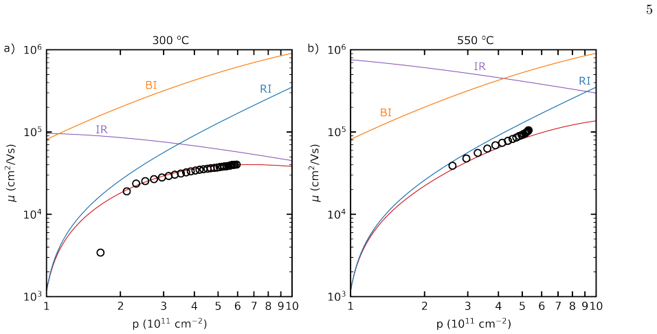
- [Modeling] Modeling subsection: the statement that mobility modeling 'indicates' the temperature-induced gain is due to reduced interface roughness scattering supplies no model equations, scattering-rate expressions, fitted parameters, or sensitivity analysis showing that other mechanisms (e.g., temperature-dependent impurity incorporation) were ruled out or held constant; this attribution is load-bearing for the optimization conclusion.
- [Results] Results section: the reported peak mobility is given as a single value without error bars, number of samples, or statistics on reproducibility, which is required to substantiate the central experimental claim when the abstract itself notes the absence of raw data and sample statistics.
minor comments (2)
- [Methods] Methods section: growth rates, buffer thicknesses, and exact temperature set-points should be tabulated for reproducibility.
- [Figures] Figure captions: mobility vs. density or temperature plots would benefit from explicit labeling of the optimized vs. non-optimized samples.
Simulated Author's Rebuttal
We thank the referee for the constructive feedback on our manuscript. We address each major comment below and indicate where revisions will be made to strengthen the presentation.
read point-by-point responses
-
Referee: [Abstract / Results] Abstract and Results section: the headline claim that 105,000 cm²/Vs represents the highest mobility for shallow MBE-grown samples is unsupported because no table or explicit list of prior literature values (with matched well depth, carrier density, and measurement temperature) is provided; without this, the assertion that prior MBE samples were limited by suboptimal conditions cannot be evaluated.
Authors: We agree that an explicit, matched comparison table is needed to support the claim. In the revised manuscript we will add a table (in the Results section or as supplementary material) listing prior MBE-grown shallow Ge quantum-well mobilities together with well depth, carrier density, and measurement temperature. This will allow direct evaluation of the literature comparison and the statement that our optimized growth yields the highest reported value for such samples. revision: yes
-
Referee: [Modeling] Modeling subsection: the statement that mobility modeling 'indicates' the temperature-induced gain is due to reduced interface roughness scattering supplies no model equations, scattering-rate expressions, fitted parameters, or sensitivity analysis showing that other mechanisms (e.g., temperature-dependent impurity incorporation) were ruled out or held constant; this attribution is load-bearing for the optimization conclusion.
Authors: The modeling relies on standard 2D scattering-rate expressions, but we acknowledge that the current text does not present the equations or parameter values. We will expand the Modeling subsection (or move the details to supplementary information) to include the relevant scattering-rate formulas, the fitted parameters, and a short discussion of why interface-roughness scattering is the dominant temperature-dependent term while other mechanisms remain comparatively constant under the growth conditions explored. revision: yes
-
Referee: [Results] Results section: the reported peak mobility is given as a single value without error bars, number of samples, or statistics on reproducibility, which is required to substantiate the central experimental claim when the abstract itself notes the absence of raw data and sample statistics.
Authors: The reported peak is the highest value obtained on an optimized wafer. We will revise the Results section to state the number of samples grown and measured under the final optimized conditions and to note the range of mobilities observed, thereby providing context on reproducibility. Because the abstract already flags the absence of full raw datasets, we will keep the presentation concise while adding this clarification; full device-level statistics remain outside the scope of the present optimization-focused study. revision: partial
Circularity Check
No circularity: experimental optimization with mobility reporting and qualitative modeling attribution
full rationale
The paper reports experimental growth optimization of Ge quantum wells via MBE, including buffer layer use and temperature tuning, culminating in a measured peak hole mobility of 105,000 cm²/Vs at 2 K. The abstract states that mobility modeling 'indicates' the gain is likely due to reduced interface roughness scattering, but this is a post-hoc attribution rather than a derivation or prediction that reduces to fitted inputs by construction. No equations, self-definitional parameters, fitted inputs renamed as predictions, or load-bearing self-citations appear in the provided text. The central claim is an empirical result with literature comparison; the modeling is described only as indicative and does not form a closed loop equivalent to the inputs. This is a standard experimental materials report with no circular structure.
Axiom & Free-Parameter Ledger
Reference graph
Works this paper leans on
-
[1]
N. W. Hendrickx, W. I. L. Lawrie, L. Petit, A. Sammak, G. Scappucci, and M. Veldhorst, A single-hole spin qubit, Nature Communications11, 3478 (2020)
work page 2020
-
[2]
N. W. Hendrickx, D. P. Franke, A. Sammak, G. Scap- pucci, and M. Veldhorst, Fast two-qubit logic with holes in germanium, Nature577, 487 (2020)
work page 2020
-
[3]
N. W. Hendrickx, L. Massai, M. Mergenthaler, F. J. Schupp, S.Paredes, S.W.Bedell, G.Salis,andA.Fuhrer, Sweet-spot operation of a germanium hole spin qubit with highly anisotropic noise sensitivity, Nature Mate- rials23, 920 (2024)
work page 2024
-
[4]
F. van Riggelen-Doelman, C.-A. Wang, S. L. de Snoo, W. I. L. Lawrie, N. W. Hendrickx, M. Rimbach-Russ, A. Sammak, G. Scappucci, C. Déprez, and M. Veldhorst, Coherent spin qubit shuttling through germanium quan- tum dots, Nature Communications15, 5716 (2024)
work page 2024
-
[5]
O. Sagi, A. Crippa, M. Valentini, M. Janik, L.Baghumyan, G.Fabris, L.Kapoor, F.Hassani, J.Fink, S. Calcaterra, D. Chrastina, G. Isella, and G. Katsaros, A gate tunable transmon qubit in planar Ge, Nature Com- munications15, 6400 (2024)
work page 2024
-
[6]
E. Kiyooka, C. Tangchingchai, L. Noirot, A. Leblanc, B. Brun, S. Zihlmann, R. Maurand, V. Schmitt, E. Du- mur, J.-M. Hartmann, F. Lefloch, and S. De Franceschi, Gatemon qubit on a germanium quantum-well het- erostructure, Nano Letters25, 562 (2025)
work page 2025
-
[7]
A. Sammak, D. Sabbagh, N. W. Hendrickx, M. Lodari, B. Paquelet Wuetz, A. Tosato, L. R. Yeoh, M. Bollani, M. Virgilio, M. A. Schubert, P. Zaumseil, G. Capellini, M. Veldhorst, and G. Scappucci, Shallow and Undoped Germanium Quantum Wells: A Playground for Spin and Hybrid Quantum Technology, Advanced Functional Ma- terials29, 1807613 (2019)
work page 2019
-
[8]
D. Zhang, J.Lu, Z. Liu, F. Wan, X. Liu, Y. Pang, Y. Zhu, B. Cheng, J. Zheng, Y. Zuo, and C. Xue, Sharp interface of undoped Ge/SiGe quantum well grown by ultrahigh vacuum chemical vapor deposition, Applied Physics Let- ters121, 022102 (2022)
work page 2022
-
[9]
Z. Kong, Z. Li, G. Cao, J. Su, Y. Zhang, J. Liu, J. Liu, Y. Ren, H. Li, L. Wei, G.-p. Guo, Y. Wu, H. H. Radam- son, J. Li, Z. Wu, H.-o. Li, J. Yang, C. Zhao, T. Ye, and G. Wang, Undoped Strained Ge Quantum Well with Ul- trahigh Mobility of Two Million, ACS Applied Electronic Materials15, 28799 (2023)
work page 2023
-
[10]
M. Myronov, J. Kycia, P. Waldron, W. Jiang, P. Bar- rios, A. Bogan, P. Coleridge, and S. Studenikin, Holes Outperform Electrons in Group IV Semiconductor Ma- terials, Small Science3, 2200094 (2023)
work page 2023
- [11]
-
[12]
F. Vigneau, R. Mizokuchi, D. C. Zanuz, X. Huang, S. Tan, R. Maurand, S. Frolov, A. Sammak, G. Scap- pucci, F. Lefloch, and S. De Franceschi, Germanium quantum-well josephson field-effect transistors and inter- ferometers, Nano Letters19, 1023 (2019)
work page 2019
- [13]
-
[14]
M. Valentini, O. Sagi, L. Baghumyan, T. de Gi- jsel, J. Jung, S. Calcaterra, A. Ballabio, J. Aguil- era Servin, K. Aggarwal, M. Janik, T. Adletzberger, R. Seoane Souto, M. Leijnse, J. Danon, C. Schrade, E. Bakkers, D. Chrastina, G. Isella, and G. Katsaros, Parity-conserving Cooper-pair transport and ideal super- conducting diode in planar germanium, Natur...
work page 2024
-
[15]
Y. H. Xie, D. Monroe, E. A. Fitzgerald, P. J. Silver- man, F. A. Thiel, and G. P. Watson, Very high mobility two-dimensional hole gas in Si/GexSi1-x/Ge structures 7 grown by molecular beam epitaxy, Applied Physics Let- ters2264, 2263 (1993)
work page 1993
-
[16]
E. Sigle, D. Weißhaupt, M. Oehme, H. S. Funk, D. Schwarz, F. Berkmann, and J. Schulze, Strained Ge Channels with High Hole Mobility Grown on Si Sub- strates by Molecular Beam Epitaxy, 2021 44th Interna- tional Convention on Information, Communication and Electronic Technology (MIPRO) , 40 (2021)
work page 2021
- [17]
-
[18]
V. Shah, A. Dobbie, M. Myronov, and D. Leadley, High quality relaxed Ge layers grown directly on a Si(001) sub- strate, Solid-State Electronics62, 189 (2011)
work page 2011
-
[19]
H. Shiraki, Elimination of Stacking Faults in Silicon Wafers by HCl Added Dry O2 Oxidation, Japanese Jour- nal of Applied Physics14, 747 (1975)
work page 1975
-
[20]
V. A. Shah, A. Dobbie, M. Myronov, and D. R. Leadley, Reverse graded SiGe/Ge/Si buffers for high-composition virtual substrates, Journal of Applied Physics107, 064304 (2010)
work page 2010
-
[21]
J. C. Bean, L. C. Feldman, A. T. Fiory, S. Nakahara, and I. K. Robinson, GexSi1-x/Si strained-layer superlat- tice grown by molecular beam epitaxy, Journal of Vac- uum Science & Technology A: Vacuum, Surfaces, and Films2, 436 (1984)
work page 1984
-
[22]
Y.-H. Su, Y. Chuang, C.-Y. Liu, J.-Y. Li, and T.-M. Lu, Effects of surface tunneling of two-dimensional hole gases in undoped Ge/GeSi heterostructures, Physical Review Materials1, 044601 (2017)
work page 2017
-
[23]
S. Das Sarma and E. H. Hwang, Universal density scaling of disorder-limited low-temperature conductivity in high- mobilitytwo-dimensionalsystems,PhysicalReviewB88, 035439 (2013)
work page 2013
-
[24]
Y. Shimura, C. Godfrin, A. Hikavyy, R. Li, J. Aguilera, G. Katsaros, P. Favia, H. Han, D. Wan, K. De Greve, and R. Loo, Compressively strained epitaxial Ge layers for quantum computing applications, Materials Science in Semiconductor Processing174, 108231 (2024)
work page 2024
-
[25]
F. Stern and W. E. Howard, Properties of Semiconductor Surface Inversion Layers in the Electric Quantum Limit, Physical Review163, 816 (1967)
work page 1967
-
[26]
J. Debdeep, A. C. Gossard, and U. K. Mishra, Disloca- tion scattering in a two-dimensional electron gas, Applied Physics Letters76, 1707 (2000)
work page 2000
-
[27]
I. Vurgaftman, M. P. Lumb, and J. R. Meyer,Bands and Photons in III-V Semiconductor Quantum Struc- tures(Oxford University Press, 2020)
work page 2020
-
[28]
J. T. Dong, Y. Gul, A. N. Engel, T. A. J. van Schijn- del, C. P. Dempsey, M. Pepper, and C. J. Palmstrøm, Enhanced mobility of ternary InGaAs quantum wells through digital alloying, Phys. Rev. Mater.8, 64601 (2024)
work page 2024
-
[29]
F. F. Fang and W. E. Howard, Negative Field-Effect Mo- bility on (100) Si Surfaces, Physical Review Letters16, 797 (1966)
work page 1966
-
[30]
A. Gold, Mobility of the two-dimensional electron gas in AlGaAs/GaAs heterostructures at low electron densities, Applied Physics Letters54, 2100 (1989)
work page 1989
-
[31]
A. Gold, Metal-insulator transition in AlxGa1-xAs/GaAs heterostructures with large spacer width, Physical Re- view B44, 8818 (1991)
work page 1991
-
[32]
A. Gold, Metal–insulator transition in Si/SiGe het- erostructures: mobility, spin polarization and Dingle temperature, Semiconductor Science and Technology26, 045017 (2011)
work page 2011
-
[33]
A. Gold, Alloy-disorder scattering of the interacting electron gas in quantum wells and heterostructures of AlxGa1-xAs, JETP Letters98, 416 (2013)
work page 2013
- [34]
discussion (0)
Sign in with ORCID, Apple, or X to comment. Anyone can read and Pith papers without signing in.