Charge transition levels of quantum emitters in hexagonal boron nitride
Pith reviewed 2026-05-25 12:14 UTC · model grok-4.3
The pith
Charge transfer to graphene measures the energy levels that set charge states of quantum emitters in hBN.
A machine-rendered reading of the paper's core claim, the machinery that carries it, and where it could break.
Core claim
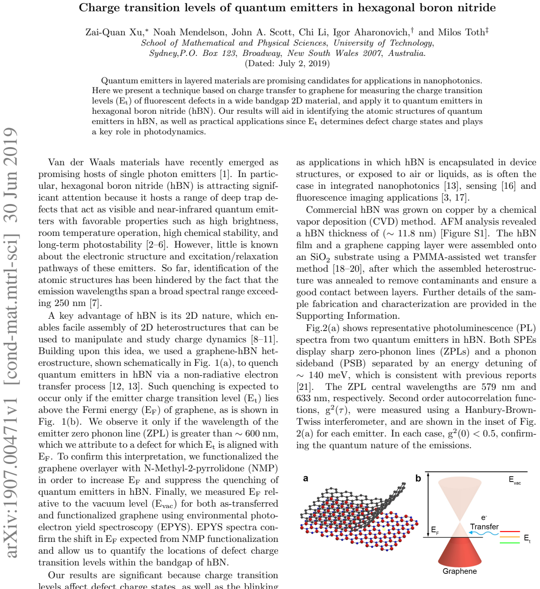
The authors establish that charge transfer to graphene supplies a direct measurement of the charge transition levels E_t of quantum emitters in hBN. These E_t values fix the defect charge state under given conditions and thereby control the photodynamics of the emitter.
What carries the argument
Charge transfer to graphene in fabricated heterostructures that reports the intrinsic E_t of the fluorescent defects.
If this is right
- The extracted E_t values narrow the possible atomic structures of the emitters.
- Device models can now predict which charge state an emitter occupies under typical operating voltages.
- Photodynamic simulations gain a concrete input for predicting blinking or ionization rates.
- The same heterostructure approach extends to other wide-bandgap 2D hosts that host fluorescent defects.
Where Pith is reading between the lines
- Graphene electrodes could be used to stabilize a chosen charge state and reduce blinking in working devices.
- The method might be combined with electrostatic force microscopy to separate interface effects from bulk defect levels.
- Similar charge-transfer readout could benchmark defect models across multiple 2D material platforms.
Load-bearing premise
The observed charge transfer between the emitters and graphene reports the intrinsic charge transition levels without significant interference from interface states, doping variations, or other electrostatic effects.
What would settle it
If the apparent transition levels shift systematically with graphene doping density or with different hBN-graphene interface preparations in ways inconsistent with a fixed intrinsic E_t, the claim would be refuted.
Figures


read the original abstract
Quantum emitters in layered materials are promising candidates for applications in nanophotonics. Here we present a technique based on charge transfer to graphene for measuring the charge transition levels ($\rm E_t$) of fluorescent defects in a wide bandgap 2D material, and apply it to quantum emitters in hexagonal boron nitride (hBN). Our results will aid in identifying the atomic structures of quantum emitters in hBN, as well as practical applications since $\rm E_t$ determines defect charge states and plays a key role in photodynamics.
Editorial analysis
A structured set of objections, weighed in public.
Referee Report
Summary. The manuscript presents a technique that uses electrostatic gating and charge transfer between hBN quantum emitters and an adjacent graphene layer to determine the charge transition levels E_t of the defects. The method is applied to fluorescent defects in hBN, with the stated goal of aiding atomic-structure identification and applications that depend on defect charge states and photodynamics.
Significance. If the mapping from gate-voltage thresholds to intrinsic E_t can be shown to be free of interface artifacts, the approach would supply a useful experimental handle on defect energetics in wide-gap 2D materials. The work does not report machine-checked derivations, reproducible code, or parameter-free predictions.
major comments (2)
- [Technique description / abstract] The central claim (abstract) that the gate-voltage position at which an emitter turns on/off directly reports the defect E_t via alignment with the graphene Fermi level rests on the untested assumption that interface states at the hBN-graphene boundary do not pin the Fermi level or open parallel charge-transfer channels. No control experiment (freestanding hBN, known bulk defects, or independent E_t measurement) is described that would falsify this interference.
- [Discussion of electrostatic environment] Local electrostatic effects (doping inhomogeneity, strain, dielectric screening) are acknowledged as possible shifts to the effective E_t, yet the manuscript provides no quantitative estimate or experimental bound on their magnitude relative to the reported E_t values.
minor comments (2)
- [Abstract / introduction] Notation for E_t is introduced without an explicit definition or diagram showing its position relative to the hBN band edges and the graphene Dirac point.
- [Abstract] The abstract states that the results 'will aid in identifying the atomic structures,' but no concrete link between measured E_t values and candidate defect models is supplied.
Simulated Author's Rebuttal
We thank the referee for the careful reading and constructive comments. We address the major comments point by point below.
read point-by-point responses
-
Referee: The central claim (abstract) that the gate-voltage position at which an emitter turns on/off directly reports the defect E_t via alignment with the graphene Fermi level rests on the untested assumption that interface states at the hBN-graphene boundary do not pin the Fermi level or open parallel charge-transfer channels. No control experiment (freestanding hBN, known bulk defects, or independent E_t measurement) is described that would falsify this interference.
Authors: We agree that the technique assumes the graphene Fermi level sets the charge-transfer threshold without dominant interference from interface states. Direct controls such as freestanding hBN are incompatible with the charge-transfer method itself. However, the observed sharp, reproducible on/off transitions across multiple emitters provide indirect support that pinning is not the dominant mechanism. We will revise the manuscript to expand the discussion section with literature references on hBN-graphene interfaces (where Fermi-level pinning is typically weak) and to state the assumption and its possible limitations more explicitly. revision: partial
-
Referee: Local electrostatic effects (doping inhomogeneity, strain, dielectric screening) are acknowledged as possible shifts to the effective E_t, yet the manuscript provides no quantitative estimate or experimental bound on their magnitude relative to the reported E_t values.
Authors: The referee correctly notes the absence of quantitative bounds. In the revised manuscript we will add order-of-magnitude estimates drawn from the literature for typical strain, doping inhomogeneity, and dielectric screening shifts in hBN-graphene heterostructures, and compare these to the spread of our measured E_t values. This will give readers a clearer sense of the uncertainty. revision: yes
Circularity Check
No circularity: experimental measurement technique with no self-referential derivations
full rationale
The paper describes an experimental method to measure charge transition levels Et of defects in hBN via charge transfer to graphene. No equations, fitted parameters renamed as predictions, self-citation load-bearing arguments, or ansatzes appear in the abstract or method description. The central claim is an empirical mapping from observed on/off voltages to Et, which does not reduce to its own inputs by construction. No derivation chain exists to inspect for circularity.
Axiom & Free-Parameter Ledger
Reference graph
Works this paper leans on
-
[1]
M. Toth and I. Aharonovich, Annual Review of Physical Chemistry 70, 123 (2019)
work page 2019
-
[2]
T. T. Tran, K. Bray, M. J. Ford, M. Toth, and I. Aharonovich, Nature nanotechnology 11, 37 (2016)
work page 2016
-
[3]
M. Kianinia, C. Bradac, B. Sontheimer, F. Wang, T. T. Tran, M. Nguyen, S. Kim, Z.-Q. Xu, D. Jin, A. W. Schell, et al. , Nature communications 9, 874 (2018)
work page 2018
-
[4]
A. L. Exarhos, D. A. Hopper, R. R. Grote, A. Alkauskas, and L. C. Bassett, ACS nano 11, 3328 (2017)
work page 2017
- [5]
-
[6]
L. Mart´ ınez, T. Pelini, V. Waselowski, J. Maze, B. Gil, G. Cassabois, and V. Jacques, Physical Review B 94, 121405 (2016)
work page 2016
-
[7]
N. R. Jungwirth, B. Calderon, Y. Ji, M. G. Spencer, M. E. Flatt´ e, and G. D. Fuchs, Nano letters 16, 6052 (2016)
work page 2016
-
[8]
Y. Liu, H. Fang, A. Rasmita, Y. Zhou, J. Li, T. Yu, Q. Xiong, N. Zheludev, J. Liu, and W. Gao, Science advances 5, eaav4506 (2019)
work page 2019
-
[9]
C. Jin, J. Kim, J. Suh, Z. Shi, B. Chen, X. Fan, M. Kam, K. Watanabe, T. Taniguchi, S. Tongay, et al. , Nature Physics 13, 127 (2017)
work page 2017
-
[10]
D. Wong, J. Velasco Jr, L. Ju, J. Lee, S. Kahn, H.-Z. Tsai, C. Germany, T. Taniguchi, K. Watanabe, A. Zettl, et al. , Nature nanotechnology 10, 949 (2015)
work page 2015
-
[11]
N. Mendelson, Z.-Q. Xu, T. T. Tran, M. Kianinia, J. Scott, C. Bradac, I. Aharonovich, and M. Toth, ACS nano 13, 3132 (2019)
work page 2019
-
[12]
K. Tielrooij, L. Orona, A. Ferrier, M. Badioli, G. Nav- ickaite, S. Coop, S. Nanot, B. Kalinic, T. Cesca, L. Gau- dreau, et al. , Nature Physics 11, 281 (2015)
work page 2015
-
[13]
K. G. Schdler, C. Ciancico, S. Pazzagli, P. Lombardi, A. Bachtold, C. Toninelli, A. Reserbat-Plantey, and F. H. Koppens, Nano letters (2019)
work page 2019
-
[14]
Z.-Q. Xu, C. Elbadawi, T. T. Tran, M. Kianinia, X. Li, D. Liu, T. B. Hoffman, M. Nguyen, S. Kim, J. H. Edgar, et al. , Nanoscale 10, 7957 (2018)
work page 2018
-
[15]
X. Li, G. D. Shepard, A. Cupo, N. Camporeale, K. Shayan, Y. Luo, V. Meunier, and S. Strauf, ACS nano 11, 6652 (2017)
work page 2017
-
[16]
T. T. Tran, B. Regan, E. A. Ekimov, Z. Mu, Y. Zhou, W.-b. Gao, P. Narang, A. S. Solntsev, M. Toth, I. Aharonovich, and C. Bradac, Science Advances 5 (2019), 10.1126/sciadv.aav9180
- [17]
-
[18]
T. T. Tran, D. Wang, Z.-Q. Xu, A. Yang, M. Toth, T. W. Odom, and I. Aharonovich, Nano letters 17, 2634 (2017)
work page 2017
-
[19]
R. Wang, D. G. Purdie, Y. Fan, F. C.-P. Mass- abuau, P. Braeuninger-Weimer, O. J. Burton, R. Blume, R. Schloegl, A. Lombardo, R. S. Weatherup, et al. , ACS nano 13, 2114 (2019)
work page 2019
-
[20]
J. Feng, H. Deschout, S. Caneva, S. Hofmann, I. Lon?ari?, P. Lazi?, and A. Radenovic, Nano letters 18, 1739 (2018)
work page 2018
-
[21]
T. T. Tran, C. Elbadawi, D. Totonjian, C. J. Lobo, G. Grosso, H. Moon, D. R. Englund, M. J. Ford, I. Aharonovich, and M. Toth, ACS nano 10, 7331 (2016)
work page 2016
-
[22]
L. Gaudreau, K. Tielrooij, G. Prawiroatmodjo, J. Os- mond, F. G. de Abajo, and F. Koppens, Nano letters 13, 2030 (2013)
work page 2030
-
[23]
A. Scavuzzo, S. Mangel, J.-H. Park, S. Lee, D. Loc Duong, C. Strelow, A. Mews, M. Burghard, and K. Kern, Applied Physics Letters 114, 062104 (2019)
work page 2019
-
[24]
T. W. Shanley, A. A. Martin, I. Aharonovich, and M. Toth, Applied Physics Letters 105, 063103 (2014)
work page 2014
-
[25]
K. Xu, C. Zeng, Q. Zhang, R. Yan, P. Ye, K. Wang, A. C. Seabaugh, H. G. Xing, J. S. Suehle, C. A. Richter, et al., Nano letters 13, 131 (2012)
work page 2012
-
[26]
A. Das, S. Pisana, B. Chakraborty, S. Piscanec, S. K. Saha, U. V. Waghmare, K. S. Novoselov, H. R. Krishna- murthy, A. K. Geim, A. C. Ferrari, et al. , Nature Nan- otechnology 3, 210 (2008)
work page 2008
- [27]
-
[28]
H. K. Choi, J. Park, N. Myoung, H.-J. Kim, J. S. Choi, Y. K. Choi, C.-Y. Hwang, J. T. Kim, S. Park, Y. Yi, et al. , Nanoscale 9, 18644 (2017)
work page 2017
-
[29]
H. L. Stern, R. Wang, Y. Fan, R. Mizuta, J. C. Stewart, L.-M. Needham, T. D. Roberts, R. Wai, N. S. Ginsberg, D. Klenerman, et al. , ACS nano (2019)
work page 2019
-
[30]
L. Ju, J. Velasco Jr, E. Huang, S. Kahn, C. Nosiglia, H.- Z. Tsai, W. Yang, T. Taniguchi, K. Watanabe, Y. Zhang, et al. , Nature nanotechnology 9, 348 (2014)
work page 2014
-
[31]
A. Brenneis, L. Gaudreau, M. Seifert, H. Karl, M. S. Brandt, H. Huebl, J. A. Garrido, F. H. Koppens, and A. W. Holleitner, Nature nanotechnology 10, 135 (2015)
work page 2015
discussion (0)
Sign in with ORCID, Apple, or X to comment. Anyone can read and Pith papers without signing in.