REVIEW 7 minor 40 references
Molecular Beam Epitaxy Growth of Scandium Nitride on Hexagonal SiC, GaN, and AlN
T0 review · 0 major / 7 minor · reviewed 2026-08-14 · deepseek-v4-flash
Pith's one-line read Plasma-assisted MBE of scandium nitride on hexagonal GaN, AlN, and 6H-SiC produces smooth, twinned cubic rocksalt films with (111) orientation and degenerate n-type conduction.
desk verdict Solid MBE growth study with first ScN-on-AlN and twinned-cubic (111) ScN evidence; publish after minor revision. read the letter →
The pith
A machine-rendered reading of the paper's core claim, the machinery that carries it, and where it could break.
The reading
What carries the argument
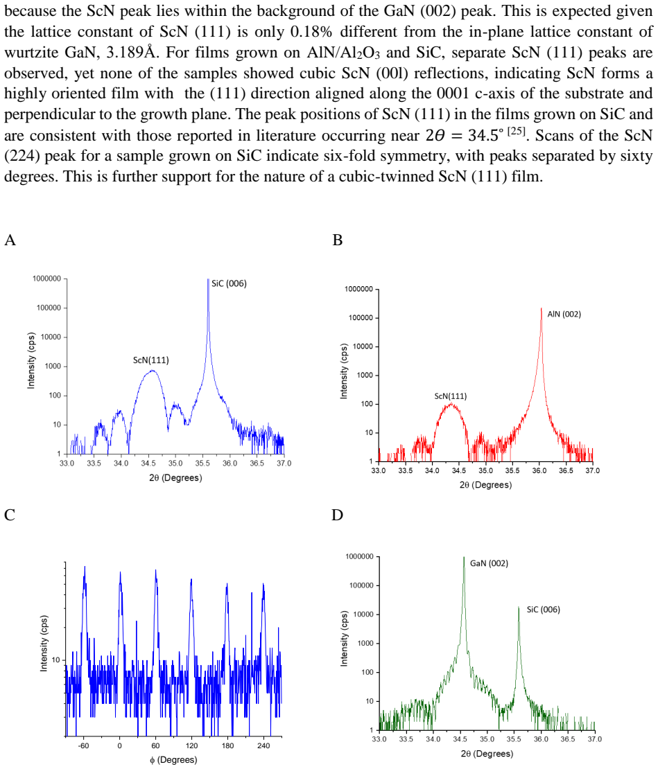
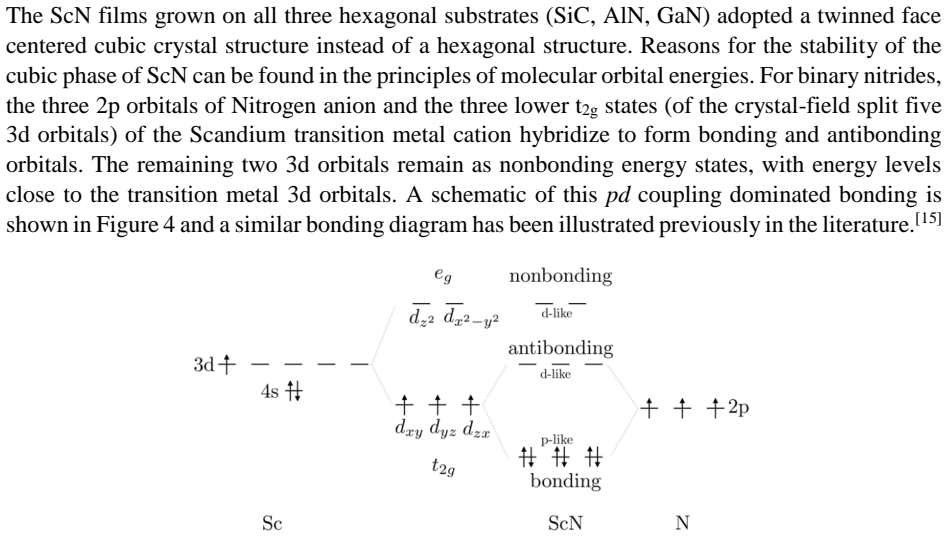
The load-bearing observation is the in-situ RHEED signature: during growth on the (110) azimuth, the hexagonal substrate's first-order streaks evolve into pairs of symmetric spots indexed as (111) and (002) reflections of a face-centered cubic lattice, giving four spots on each side of the zone center instead of two. This pattern, previously reported for twinned Cu(111) films on sapphire, is the signature of a (111)-oriented cubic crystal with twin domains. The twinned microstructure is corroborated by EBSD pole figures showing sixfold (111) symmetry and by ScN (224) $\varphi$ scans with six peaks separated by 60 degrees. The paper also uses a molecular-orbital bonding diagram in which the three outer electrons of Sc fill bonding states formed by N 2p and the crystal-field-split $t_{2g}$ orbitals, leaving the antibonding states empty, to explain why the cubic phase is stable even when grown on hexagonal substrates.
What would settle it
Cross-sectional transmission electron microscopy and reciprocal-space mapping of the ScN/GaN and ScN/AlN interfaces, combined with a high-resolution scan for non-(111) reflections such as ScN (200) or (220), would reveal whether minority orientations or secondary phases exist; a companion measurement of oxygen concentration versus carrier density would test the oxygen-donor explanation.
Extended reading notes
Core claim
The paper argues that scandium nitride grown by plasma-assisted MBE on c-plane GaN, AlN, and 6H-SiC does not adopt a hexagonal structure but instead forms a face-centered cubic rocksalt phase oriented with the (111) direction parallel to the substrate 0001 c-axis. The films are entirely (111) oriented with twinned in-plane domains, a conclusion supported by the appearance of paired (111) and (002) spots in RHEED, by two-color striped EBSD topography with sixfold {111} pole figures, and by sixfold symmetry in ScN (224) X-ray $\varphi$ scans. The films show sub-nanometer RMS roughness at the 750°C growth temperature, and Hall measurements give a temperature-independent n-type carrier concentration near $1\times10^{20}$ cm$^{-3}$ with mobilities around 20 cm$^2$/Vs, indicating degenerate doping. The paper interprets the stability of the rocksalt phase through a molecular-orbital picture in which N 2p and Sc $t_{2g}$ orbitals hybridize to fill bonding states, and it attributes the high carrier density primarily to oxygen impurities while noting that the polar/nonpolar interface may also contribute mobile charge.
Load-bearing premise
The conclusion that every ScN grain is single-phase cubic rocksalt with only (111) out-of-plane orientation and twin-related in-plane domains rests on surface and diffraction evidence rather than direct cross-sectional imaging; a hidden minority orientation, secondary phase, or interfacial layer would weaken the central claim.
Editorial extensions
If this is right
- Because ScN(111) is nearly lattice-matched to GaN(0001), the cubic (111) orientation is the expected epitaxial relationship even where the ScN(111) XRD peak is masked by the GaN(002) reflection.
- The temperature-independent carrier concentration near $10^{20}$ cm$^{-3}$ means the as-grown ScN layers behave as degenerate metallic conductors, so contact and buffer applications do not require intentional doping.
- The first MBE growth of ScN on AlN provides a limiting binary datum for the ScAlN alloy system, whose piezoelectric and ferroelectric properties depend on Sc content.
- The twinned (111) microstructure, with 60-degree rotated domains, is the natural product of growing a threefold-symmetric cubic plane on a sixfold-symmetric hexagonal surface; the domain size depends on the substrate and may be tunable.
Reading between the lines
- If oxygen is the dominant donor, exposing the growth surface to a controlled oxygen flux during MBE should increase the electron concentration in a predictable way, and switching to higher-purity Sc sources should lower it.
- A cross-sectional TEM study comparing ScN on GaN, AlN, and SiC could determine whether twin-domain size is set by substrate step-terrace spacing or by threading dislocations, a question the paper leaves open.
- The polar/nonpolar interface at ScN/GaN and ScN/AlN may itself supply mobile charge; growing ScN on nonpolar or isostructural cubic substrates would separate interface contributions from bulk impurity doping.
Signed reviews
Editorial analysis
A structured set of objections, weighed in public.
Referee Report
Summary. This manuscript reports plasma-assisted MBE growth of ~30 nm ScN films on c-plane GaN/SiC, AlN/Al2O3, and 6H-SiC substrates, and characterizes their structure, surface morphology, and transport. The central claim is that ScN adopts the rocksalt (cubic) structure with exclusive (111) out-of-plane orientation and two twin-related in-plane domains on all three hexagonal substrates. Supporting evidence includes in-situ RHEED patterns with paired (111)/(002) spots, EBSD indexing to Fm-3m ScN with 60° in-plane misorientation, XRD 2theta-omega and phi scans on SiC and AlN, and AFM showing sub-nm roughness. Hall measurements on GaN/SiC and AlN/Al2O3 show temperature-independent n-type carrier concentrations near 1×10^20 cm^-3 with mobilities of 11–23 cm^2/Vs, interpreted as degenerate doping. The paper also offers qualitative bonding arguments for the stability of rocksalt ScN and speculates about polar/non-polar interface charges as a possible source of mobile carriers.
Significance. The structural result is significant for the III-nitride community because (111) ScN is nearly lattice-matched to GaN and is the limiting binary for emerging ScAlN/GaScN ferroelectric and piezoelectric heterostructures. The manuscript's main strengths are the complementary, mutually consistent characterization (RHEED, EBSD, XRD phi scans), the explicit and honest disclosure of the unresolved ScN (111) reflection on GaN templates, and the electrical measurement on an insulating AlN/Al2O3 substrate, which independently supports the degenerate carrier concentration. The paper makes no over-claim about the origin of the carriers; the polar-interface explanation is clearly labeled speculative, and the need for TEM is acknowledged. These factors make the central claim credible even though composition, stoichiometry, and minority-phase exclusion are not exhaustively addressed.
minor comments (7)
- [§2 (EBSD)] The sentence 'Grain misorientation statistics (not shown) indicated the ScN epitaxial film was entirely (111) oriented' is central to the exclusive-orientation claim, especially for the GaN template where XRD is inconclusive; please either include these statistics as a figure/table or provide a summary in the text.
- [§3 (XRD, Fig. 3C)] The unresolved ScN (111) reflection on GaN/SiC is disclosed in the XRD section, but the conclusions repeat the claim of 'solely cubic twinned (111) orientation' without repeating this caveat; please add one sentence in the conclusions noting that the GaN-based assignment relies on RHEED and EBSD, not XRD.
- [§2 (XPS/absorption)] The text states that 'XPS results (not shown)' verify Sc–N bonding and that 'optical absorption measurements (not shown)' show a band edge near 2.1 eV; these data should either be presented in a supplementary figure or the statements removed, because claims based on unavailable data cannot be evaluated.
- [§3 (Hall and AFM)] Report error bars or measurement uncertainties for the Hall carrier concentration, Hall mobility, and rms roughness values; single-point values are not sufficient for quantitative comparison with literature.
- [§3 (Hall on GaN)] Please state whether the GaN template could contribute a parallel conduction path in the ScN/GaN Hall measurement; the similarity of the carrier concentration to the AlN/Al2O3 sample suggests this is not a problem, but the assumption should be made explicit.
- [Fig. 2 caption] In the caption, 'domains with 180˚ orientation device' appears to be a typo for '180° orientation difference'; please correct it.
- [Acknowledgments] The grant number is listed as 'AFSOR FA9550-17-1-0048'; the standard abbreviation is AFOSR, so please correct the agency name.
Circularity Check
No significant circularity: the structural and electrical claims rest on mutually consistent RHEED, EBSD, XRD, and Hall measurements, with self-citations used only for motivation and a clearly labeled speculative interface explanation.
full rationale
This is an experimental growth and characterization paper. The central claims are that ScN grown on GaN, AlN, and SiC adopts a cubic rocksalt (111) twinned orientation and is degenerately n-type doped. These claims are built from direct measurements: in-situ RHEED patterns showing paired (111) and (002) spots associated with cubic twinning, EBSD Kikuchi indexing to Fm-3m ScN with dominant 60-degree in-plane misorientation, XRD 2theta-omega and phi scans showing (111) orientation and sixfold symmetry, and temperature-independent Hall data. No parameter is fitted to a subset of data and then relabeled as a prediction. The paper honestly discloses that on GaN/SiC the ScN (111) XRD peak overlaps the GaN (002) peak, so for that substrate the phase and orientation assignment depends on RHEED and EBSD; this is a limitation, not a circular step. The only self-citations are reference [1], used as general motivation for nitride-compatible materials, and reference [40], used to suggest a possible polar-discontinuity origin for mobile carriers. Both are non-load-bearing: the structural result does not depend on them, and the electrical result is directly measured by Hall effect, with the polar-interface mechanism explicitly offered as a speculation to be tested by future work, not as the basis of the measurement. There is no derivation, no imported uniqueness theorem, and no ansatz smuggled in via self-citation. The paper is self-contained against its own data and external literature, so no circularity is found.
Assumptions & free parameters
assumptions (4)
- domain assumption ScN equilibrium phase is rocksalt with lattice constant 4.505 A
- domain assumption Nitrogen-rich growth conditions suppress nitrogen vacancies and maintain 1:1 Sc:N stoichiometry
- domain assumption RHEED spot pairs indexed as rotated (1-10) zone axes indicate cubic twinning
- domain assumption EBSD Kikuchi patterns indexed to FCC ScN (Fm-3m) are sufficient to determine film orientation
Cite this review
Pith. "Pith review of Molecular Beam Epitaxy Growth of Scandium Nitride on Hexagonal SiC, GaN, and AlN." pith.science (2026). https://pith.science/paper/M5SUPZHF
@misc{pith2026190801045,
  author       = {Pith},
  title        = {Pith review of: Molecular Beam Epitaxy Growth of Scandium Nitride on Hexagonal SiC, GaN, and AlN},
  year         = {2026},
  howpublished = {\url{https://pith.science/paper/M5SUPZHF}},
  note         = {Machine review of arXiv:1908.01045}
}
read the original abstract
RF plasma assisted MBE growth of Scandium Nitride (ScN) thin films on GaN (0001)/SiC, AlN (0001)/Al2O3 and on 6H-SiC (0001) hexagonal substrates is found to lead to a face centered cubic (rock-salt) crystal structure with (111) out-of-plane orientation instead of hexagonal orientation. For the first time, cubic (111) twinned patterns in ScN are observed by in-situ electron diffraction during epitaxy, and the twin domains in ScN are detected by electron backscattered diffraction, and further corroborated with X-ray diffraction. The epitaxial ScN films display very smooth, sub nanometer surface roughness at a growth temperature of 750C. Temperature-dependent Hall-effect measurements indicate a constant high n-type carrier concentration of ~1x10²⁰/cm3 and electron mobilities of ~ 20 cm2/Vs.
Figures

Figures from the paper (1 more)

Reference graph
Works this paper leans on
-
[1]
D. Jena, R. Page, J. Casamento, P. Dang, J. Singhal, Z. Zhang, J. Wright, G. Khalsa, Y. Cho, and H.G Xing, Jpn. J. Appl. Phys. 58, SC0801 (2019)
work page 2019
- [2]
- [3]
-
[4]
B. Saha, G.V Naik, S. Saber, C. Akatay, E.A Stach, V. Shalaev, A. Boltasevva, and T.D Sands, Phys. Rev. B. 90, 125420 (2014)
work page 2014
-
[5]
S. Kerdsongpanya, N. Van Nong, N. Pryds, A. Žukauskaite, J. Jensen, J. Birch, J. Lu, L. Hultman, G. Wingqvist, and P. Eklund, Appl. Phys. Lett. 99, 232133 (2011)
work page 2011
-
[6]
B. Saha, M. Garbrecht, J.A Perez-Taborda, M.H Fawey, Y.R Koh, A. Shakouri, M. Martin- Gonzalez, L. Hultman, and T.D Sands, Appl. Phys. Lett. 110, 252104 (2017)
work page 2017
-
[7]
Teshigahara, K.Y Hashimoto, and M
A. Teshigahara, K.Y Hashimoto, and M. Akiyama, IEEE International Ultrasonics Symposium IUS (2013)
work page 2013
-
[8]
M. Akiyama, T. Kamohara, K. Kano, A. Teshigahara, Y. Takeuchi, and N. Kawahara, Appl. Phys. Lett. 95, 162107 (2009)
work page 2009
Show all 40 references
-
[9]
Zhang, D
S. Zhang, D. Holec, W.Y Fu, C.J Humphreys, and M.A Moram, J. Appl. Phys. 114, 133510 (2013)
2013
-
[10]
Zhang, J
M.A Moram and S. Zhang, J. Mater. Chem. A. 2, 6042 (2014)
2014
-
[11]
Fichtner, N
S. Fichtner, N. Wolff, F. Lofink, L. Kienle, and B. Wagner, J. Appl. Phys. 125, 114103 (2019)
2019
-
[12]
Nepal, D.F Storm, D.S Katzer, and D.J Meyer, Appl
M.T Hardy, B.P Downey, N. Nepal, D.F Storm, D.S Katzer, and D.J Meyer, Appl. Phys. Lett. 110, 162104 (2017)
2017
-
[13]
Nepal, D.F Storm, and D.S Katzer, IEEE Trans
M.T Hardy, B.P Downey, D.J Meyer, N. Nepal, D.F Storm, and D.S Katzer, IEEE Trans. Semiond. Manufact. 30, 475 (2017)
2017
-
[14]
D. Gall, I. Petrov, N. Hellgren, L. Hultman, J.E Sundgren, and J.E Greene, J. Appl. Phys. 84, 6034 (1998)
1998
-
[15]
Qteish, P
A. Qteish, P. Rinke, M. Scheffler, and J. Neugebauer, Phys. Rev. B. 74, 245208 (2006)
2006
-
[16]
Samsonov, M
G. Samsonov, M. Lyutaya, and V. Neshpor, Zh. Prikl. Khimii 36, 2108 (1963)
1963
-
[17]
Moram, Z
M. Moram, Z. Barber, C. Humphreys, T. Joyce, and P. Chalker, J. Appl. Phys. 100, 23514 (2006)
2006
-
[18]
Inorganic Crystal Structure Database
-
[19]
Nörenberg, C.T Foxon, and C.J Humphreys, J
M.A Moram, S.V Novikov, A.J Kent, C. Nörenberg, C.T Foxon, and C.J Humphreys, J. Cryst. Growth 310, 2746 (2008)
2008
-
[20]
Zhang, Z.H Barber, and C.J Humphreys, Phys
M.A Moram, M.J Kappers, Y. Zhang, Z.H Barber, and C.J Humphreys, Phys. Stat. Sol. (A) 205, 1064 (2008)
2008
-
[21]
M.A Moram, T.B Joyce, P.R Chalker, Z.H Barber, and C.J Humphreys, Appl. Surf. Sci. 252, 8385 (2006)
2006
-
[22]
Lupina, M.H Zoellner, T
L. Lupina, M.H Zoellner, T. Niermann, B. Dietrich, G. Capellini, S.B Thapa, M. Haeberlen, M. Lehmann, P. Storck, and T. Schroeder, Appl. Phys. Lett. 107, 201907 (2015)
2015
-
[23]
Al-Brithen and A.R Smith, Appl
H. Al-Brithen and A.R Smith, Appl. Phys. Lett. 77, 2485 (2000)
2000
-
[24]
T.D Moustakas, R.J Molnar, and J.P Dismukes, Electrochemical Society Proceedings 96, 197 (1996)
1996
-
[25]
Bohnen, and P.R Hageman, J
J.H Edgar, T. Bohnen, and P.R Hageman, J. Cryst. Growth 310, 1075 (2008)
2008
-
[26]
le Febvrier, N
A. le Febvrier, N. Tureson, N. Stilkerich, G. Greczynski, and P. Eklund, J. Phys. D. Appl. Phys. 52, 035302 (2019). 11
2019
-
[27]
J.M Gregorie, S.D Kirby, G.D Scopelianos, F.H Lee, and R.B van Dover, J. Appl. Phys 104, 074913 (2008)
2008
-
[28]
Ohgaki, I
T. Ohgaki, I. Sakaguchi, N. Ohashi, and H. Haneda, J. Cryst. Growth 476, 12 (2017)
2017
-
[29]
J.P Dismukes, W.M Yin, and V.S Ban, J. Cryst. Growth 13/14, 365 (1972)
1972
-
[30]
S.W King, R.F Davis, and R.J Nemanich, J. Vac. Sci. & Tech. A. 32, 061504 (2014)
2014
-
[31]
Oshima, E.G Villora, and K
Y. Oshima, E.G Villora, and K. Shimamura, J. Appl. Phys. 115, 153508 (2014)
2014
-
[32]
Hamad, H
A.R Smith, A. Hamad, H. Al-Brithen, D.C. Ingram, and D. Gall, J. Appl. Phys. 90, 1809 (2001)
2001
-
[33]
D.L Miller, M.W Keller, J.M Shaw, A.N Chiaramonti, and R.R Keller, J. Appl. Phys. 112, 064317 (2012)
2012
-
[34]
Deng, B.D Ozsdolay, P.Y Zheng, S.V Khare, and D
R. Deng, B.D Ozsdolay, P.Y Zheng, S.V Khare, and D. Gall, Phys. Rev. B. 91, 045104 (2015)
2015
-
[35]
Daneu, A
N. Daneu, A. Rečnik, T. Yamazaki, and T. Dolenec, Phys. Chem. Miner. 34, 233 (2007)
2007
-
[36]
Cetnar, A
J. Cetnar, A. Reed, S. Badescu, S. Vangala, H. Smith, and D. Look, Appl. Phys. Lett 113, 192104 (2018)
2018
-
[37]
CRC Press
W.M Haynes, CRC Handbook of Chemistry and Physics, 96th Edition. CRC Press. (2015)
2015
-
[38]
Ohgaki, K
T. Ohgaki, K. Watanabe, Y. Adachi, I. Sakaguchi, S. Hishita, N. Ohashi, and H. Haneda, J. Appl. Phys. 114, 093704 (2013)
2013
-
[39]
Rhode, K
C.A Neidermeier, S. Rhode, K. Ide, H. Hiramatsu, H. Hosono, T. Kamiya, and M.A Moram, Phys. Rev. B. 95, 161202 (2017)
2017
-
[40]
C. Wood, D. Jena. Polarization Effects in Semiconductors -From Ab Initio Theory to Device Applications. Springer (2008)
2008
Reviewed August 14, 2026 · model on record in the stance chip above.
Discussion (0). Continue with ORCID to comment.