REVIEW 2 major objections 4 minor 57 references
Route to high hole mobility in GaN via reversal of crystal-field splitting
T0 review · 2 major / 4 minor · reviewed 2026-08-14 · deepseek-v4-flash
Pith's one-line read Stretching GaN by 2% reorders its hole bands and lifts the room-temperature Hall mobility to about 120 cm²/Vs.
desk verdict A well-executed first-principles BTE study predicting a large hole-mobility gain in GaN via strain-induced reversal of crystal-field splitting; the bulk physics is credible, but the proposed 7 nm thin-film realization leaves the confined mobility uncomputed. read the letter →
The pith
A machine-rendered reading of the paper's core claim, the machinery that carries it, and where it could break.
The reading
What carries the argument
The load-bearing object is the crystal-field splitting Δcf, the energy separation between the split-off hole band and the light/heavy hole bands at the valence-band top of wurtzite GaN. In the wurtzite structure this splitting is controlled by the internal parameter u and the c/a ratio; a distortion that lowers c/a, such as 2% biaxial tension in the basal plane or uniaxial compression along the c axis, reverses its sign and reorders the valence bands. The argument runs through the self-consistent Boltzmann transport equation with all electron-phonon couplings and GW quasiparticle band structures: the reversal changes the character of the valence-band maximum from N-px,y to N-pz states, replacing the heavy-mass final states with a lighter, strongly non-parabolic split-off band, and thereby suppressing the long-wavelength acoustic-phonon scattering that dominates hole relaxation.
What would settle it
Grow a roughly 7 nm wurtzite GaN layer under about 2% biaxial tensile strain on a substrate such as 6H-SiC or AlN, confirm the strain by X-ray diffraction, and measure the Hall hole mobility at 300 K. If the mobility does not rise to about 120 cm²/Vs, or if polarization-resolved emission shows the valence-band ordering has not inverted, the central claim fails; a null result from a film that has relaxed through dislocations would not count, since the argument requires coherent strain.
Extended reading notes
Core claim
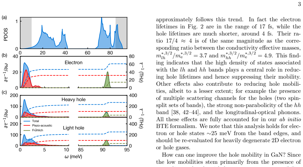
The central discovery is a mechanism, not a material tuning guess. In unstrained wurtzite GaN, the valence-band maximum is formed by the light-hole and heavy-hole bands, whose heavy masses create a high density of final states for low-energy acoustic phonons; scattering into those states suppresses hole lifetimes to about 4 fs. The paper shows that reversing the sign of the crystal-field splitting Δcf, achieved by 2% biaxial tensile strain or by uniaxial compression along the c axis, lifts the split-off band above the light and heavy holes. The new top band is lighter and strongly non-parabolic, with an effective mass near 0.45me at Γ that drops to about 0.22me away from Γ, so the dominant scattering channel is cut off. The computed consequence is a room-temperature hole Hall mobility of about 120 cm²/Vs versus about 50 cm²/Vs unstrained, with 620 cm²/Vs at 100 K, and the mobility tracks max(−Δcf, 0).
Load-bearing premise
The plan requires holding 2% coherent biaxial tensile strain in a GaN layer thin enough to avoid misfit dislocations—the computed critical thickness is about 7 nm—while still thick enough that transport remains bulk-like and phonon-limited.
Editorial extensions
If this is right
- At 2% biaxial tensile strain, the phonon-limited hole Hall mobility of wurtzite GaN reaches about 120 cm²/Vs at 300 K, a 230% increase over the unstrained value, and about 620 cm²/Vs at 100 K.
- The same valence-band reordering and mobility gain should be achievable with 2% uniaxial compressive strain along the c axis.
- Because the mobility tracks max(−Δcf, 0), strain that increases the conventional positive crystal-field splitting leaves the band ordering and mobility essentially unchanged; only sign reversal helps.
- The change in valence-band wavefunction character should be observable as a switch in the polarization of near-band-edge optical emission, offering a direct experimental signature of the reordering.
Reading between the lines
- A computed critical thickness of about 7 nm at 2% strain means the useful layer sits in a regime where quantum confinement, interface roughness, and strain gradients become active, so the bulk 120 cm²/Vs figure may be an upper bound rather than a device-level number.
- The same band-order-reversal strategy may transfer to other wurtzite semiconductors whose crystal-field splitting is strain-sensitive, potentially broadening the search for high-mobility p-type nitrides.
- One could test the mechanism without full mobility extraction by measuring the polarization of photoluminescence from a strained ultra-thin GaN layer: a switch from in-plane to c-axis polarization would confirm the band inversion before transport measurements confirm the mobility gain.
- Transient reversal by infrared pumping of the A1 optical phonon could make hole mobility a fast optical switch; if phonon lifetimes permit, this points toward sub-picosecond modulation of conduction in GaN.
Signed reviews
Editorial analysis
A structured set of objections, weighed in public.
Referee Report
Summary. This manuscript computes the phonon-limited electron and hole mobilities of wurtzite GaN from first principles using the ab initio Boltzmann transport equation with all electron-phonon scattering processes and GW quasiparticle band structures. The calculated Hall mobilities at 300 K (1030 cm2/Vs for electrons, 50 cm2/Vs for holes) are benchmarked against experiment (1265 and 31 cm2/Vs, respectively). The authors attribute the low hole mobility to the high density of final states in the heavy-hole and light-hole bands for long-wavelength acoustic-phonon scattering, and propose to overcome this bottleneck by reversing the sign of the crystal-field splitting so that the split-off hole band moves above the heavy and light hole bands. They predict that 2% biaxial tensile strain (or equivalent uniaxial compression) increases the hole Hall mobility to about 120 cm2/Vs at room temperature and 620 cm2/Vs at 100 K, with the same physics also suggested for dynamical control via coherent A1 phonon excitation.
Significance. If the central prediction holds, this is an important result: it identifies a microscopic mechanism for the long-standing low hole mobility in GaN and proposes a concrete, falsifiable design principle based on band-ordering inversion. The transport calculations are parameter-free in the sense that no mobility value is fitted; the agreement with experiment for unstrained GaN lends credibility to the methodology, and the prediction of a 2.4-fold mobility enhancement under strain is a sharp, testable statement. The use of the full Boltzmann equation with all electron-phonon scattering processes and GW band structures is a clear strength. The main weakness is that the proposed practical route, a strained thin film below the critical thickness, is not itself simulated; the mobility numbers come from bulk periodic calculations, so an uncomputed intermediate step separates the transport prediction from the proposed realization.
major comments (2)
- [How realistic is our proposal? / Fig. 3(d)-(f), Eqs. (1)-(3)] The headline mobility enhancement is computed for an infinite, periodically repeated bulk crystal under homogeneous strain, but the proposed realization requires a coherent film thinner than the Fischer critical thickness, stated in the text as 7 nm at 2% strain. For such a thin layer, quantum confinement shifts the hole subbands by energies of order hbar^2*pi^2/(2*m_z*L^2), roughly 4 meV for m_z ~ 1.8 m_0, which is the same energy scale as the crystal-field splitting being reversed in Fig. 3(d). Confinement can therefore alter the intended split-off-above-heavy ordering before scattering is considered, and interface roughness, remote charges, and strain gradients add scattering mechanisms absent from the bulk BTE. The manuscript acknowledges the thin-film practicalities but does not compute the confined band structure or a confined mobility. The bulk strained result may be internally correct, but the 120 cm2/Vs figure is not established for the proposed 'route,' and the authors should either compute the confined subbands and estimate confined transport, or explicitly limit the claim to bulk strained GaN and adjust the title/abstract accordingly.
- [Abstract and 'How realistic is our proposal?' section] The numerical claim '230% increase' is inconsistent with the data quoted in the paper. The unstrained calculated hole Hall mobility at 300 K is 50 cm2/Vs and the strained value is 120 cm2/Vs, so the ratio is about 2.4, which corresponds to a 140% increase (or '240% of the unstrained value'), not a 230% increase. If the comparison were to the experimental value of 31 cm2/Vs, the ratio would be about 3.9. Since this percentage appears in the abstract and in the main text, it should be corrected or clarified: 'by 230%' should be replaced with an accurate formulation such as 'by about 140%' or 'to about 2.4 times the unstrained value.'
minor comments (4)
- [Eq. (2)] There is a typographical inconsistency in Eq. (2): the term 'f^0_{nk+nqnu}' should presumably be a Fermi-Dirac occupation of the final state at k+q; please correct the notation so that the equation is unambiguous.
- [How realistic is our proposal?] The word 'wurzite' appears in the sentence 'We computed the GaN phase diagram to check that the wurzite structure remains the lowest-enthalpy phase under strain'; it should be spelled 'wurtzite'.
- [Fig. 1 and Hall factor] The Hall factor is not computed in this manuscript but is taken from the companion manuscript Ref. [25]; since the headline Hall mobilities depend on this factor, the authors should either state the numerical Hall factors used or include a short derivation to make the paper more self-contained.
- [Fig. 2 caption] The caption states that the dashed cumulative curves 'add up to the carrier scattering rate tau^{-1}'; it would be clearer to specify the axis on which this cumulative integral is read, since the left and right vertical axes have different units.
Circularity Check
No circularity: mobilities are computed from first principles; experimental values and companion-paper details are benchmarks, not fitted inputs.
full rationale
The derivation chain starts from DFT/DFPT/GW band structures and electron-phonon matrix elements, solves the linearized Boltzmann transport equation (Eqs. 1-3) without adjustable parameters, and only afterwards compares with experimental mobilities. The strained-GaN mobilities in Fig. 3(e,f) are obtained by repeating the same parameter-free calculation for strained structures; strain is chosen to reverse the crystal-field splitting, but the mobility value is computed, not fitted. Experimental hole mobility data are used only as a benchmark ('in good agreement with the measured values'), and the Hall factor is taken from the companion manuscript rather than adjusted to reproduce the target mobility. Self-citations to EPW/BTE methodology and to Ref. 25 supply numerical details and the Hall factor, but they do not define the predicted 230% enhancement; that prediction is a computed output of the stated equations. The thin-film feasibility issues discussed in the 'How realistic' section are practical implementation concerns, not circularity.
Assumptions & free parameters
assumptions (6)
- standard math The linearized Boltzmann transport equation with iterative solution (Eqs. 1-3) is a valid description of phonon-limited carrier transport in semiconductors.
- domain assumption DFT plus DFPT plus GW, as implemented in Quantum Espresso, Yambo, wannier90, and EPW, gives accurate band structures, phonons, and electron-phonon matrix elements for GaN.
- domain assumption The phonon-limited mobility from the linearized BTE captures the experimentally measured mobility of bulk GaN; any residual difference is not load-bearing.
- domain assumption At 2% biaxial strain the wurtzite phase remains the lowest-enthalpy phase and the strained film can be grown coherently without dislocations or cracks over the transport-relevant area.
- domain assumption The Hall factor computed in the companion paper remains valid for the strained structures when converting drift to Hall mobility.
- domain assumption The reversal of Delta_cf at 2% strain is robust with respect to the choice of DFT functional and GW corrections.
Cite this review
Pith. "Pith review of Route to high hole mobility in GaN via reversal of crystal-field splitting." pith.science (2026). https://pith.science/paper/LOHKWGMK
@misc{pith2026190802069,
  author       = {Pith},
  title        = {Pith review of: Route to high hole mobility in GaN via reversal of crystal-field splitting},
  year         = {2026},
  howpublished = {\url{https://pith.science/paper/LOHKWGMK}},
  note         = {Machine review of arXiv:1908.02069}
}
abstract
A fundamental obstacle toward the realization of GaN p-channel transistors is its low hole mobility. Here we investigate the intrinsic phonon-limited mobility of electrons and holes in wurtzite GaN using the ab initio Boltzmann transport formalism, including all electron-phonon scattering processes and many-body quasiparticle band structures. We predict that the hole mobility can be increased by reversing the sign of the crystal-field splitting, in such a way as to lift the split-off hole states above the light and heavy holes. We find that a 2% biaxial tensile strain can increase the hole mobility by 230%, up to a theoretical Hall mobility of 120 cm$^2$/Vs at room temperature and 620 cm$^2$/Vs at 100 K.
Figures


Reference graph
Works this paper leans on
-
[1]
F. A. Ponce and D. P. Bour, Nature 386, 351 (1997)
work page 1997
- [2]
-
[3]
T. J. Flack, B. N. Pushpakaran, and S. B. Bayne, J. Electron. Mater. 45, 2673 (2016)
work page 2016
- [4]
- [5]
-
[6]
B. N. Pantha, R. Dahal, J. Li, J. Y. Lin, H. X. Jiang, and G. Pomrenke, Appl. Phys. Lett. 92, 042112 (2008)
work page 2008
- [7]
-
[8]
R. Yan, G. Khalsa, S. Vishwanath, Y. Han, J. Wright, S. Rouvimov, D. S. Katzer, N. Nepal, B. P. Downey, D. A. Muller, et al., Nature 555, 183 (2018)
work page 2018
Show all 57 references
-
[9]
Chaudhuri, S
R. Chaudhuri, S. J. Bader, Z. Chen, D. A. Muller, H. G. Xing, and D. Jena, submitted (2018)
2018
-
[10]
S. J. Bader, R. Chaudhuri, K. Nomoto, A. Hickman, Z. Chen, H. W. Then, D. A. Muller, H. G. Xing, and D. Jena, IEEE Electr. Device L. pp. 1–1 (2018)
2018
-
[11]
Kozodoy, S
P. Kozodoy, S. Keller, S. DenBaars, and U. Mishra, J. Cryst. Growth 195, 265 (1998)
1998
-
[12]
Look, Properties, Processing and applications of Gallium Nitride and related semiconductors (INSPEC, 1999)
D. Look, Properties, Processing and applications of Gallium Nitride and related semiconductors (INSPEC, 1999)
1999
-
[13]
Rubin, N
M. Rubin, N. Newman, J. S. Chan, T. C. Fu, and J. T. Ross, Appl. Phys. Lett. 64, 64 (1994)
1994
-
[14]
Kozodoy, S
P. Kozodoy, S. P. DenBaars, and U. K. Mishra, J. Appl. Phys. 87, 770 (2000)
2000
-
[15]
Cheong, K
M. Cheong, K. Kim, N. Namgung, M. Han, G. Yang, C.- H. Hong, E.-K. Suh, K. Lim, H. Lee, and A. Yoshikawa, J. Cryst. Growth 221, 734 (2000)
2000
-
[16]
M. G. Cheong, K. S. Kim, C. S. Kim, R. J. Choi, H. S. Yoon, N. W. Namgung, E.-K. Suh, and H. J. Lee, Appl. Phys. Lett. 80, 1001 (2002)
2002
-
[17]
Horita, S
M. Horita, S. Takashima, R. Tanaka, H. Matsuyama, K. Ueno, M. Edo, T. Takahashi, M. Shimizu, and J. Suda, J. J. Appl. Phys. 56, 031001 (2017)
2017
-
[18]
E. C. H. Kyle, S. W. Kaun, P. G. Burke, F. Wu, Y.-R. Wu, and J. S. Speck, J. Appl. Phys. 115, 193702 (2014)
2014
-
[19]
Ponc´ e, E
S. Ponc´ e, E. R. Margine, and F. Giustino, Phys. Rev. B 97, 121201 (2018)
2018
-
[20]
Ziman, Electrons and Phonons (Oxford University Press, 1960)
J. Ziman, Electrons and Phonons (Oxford University Press, 1960)
1960
-
[21]
Li, Phys
W. Li, Phys. Rev. B 92, 075405 (2015)
2015
-
[22]
Xiao, M.-C
D. Xiao, M.-C. Chang, and Q. Niu, Rev. Mod. Phys. 82, 1959 (2010)
2010
-
[23]
Grimvall, The electron-phonon interaction in metals (North-Holland Publishing Company, 1981)
G. Grimvall, The electron-phonon interaction in metals (North-Holland Publishing Company, 1981)
1981
-
[24]
Giustino, Rev
F. Giustino, Rev. Mod. Phys. 89, 015003 (2017)
2017
-
[25]
Ponc´ e, D
S. Ponc´ e, D. Jena, and F. Giustino, arXiv:1908.02072 (2019), URL https://arxiv.org/abs/1908.02072
2019 arXiv
-
[26]
Giannozzi, O
P. Giannozzi, O. Andreussi, T. Brumme, O. Bunau, M. B. Nardelli, M. Calandra, R. Car, C. Cavazzoni, D. Ceresoli, M. Cococcioni, et al., J. Phys-Condens. Mat. (2017)
2017
-
[27]
Marini, C
A. Marini, C. Hogan, M. Grning, and D. Varsano, Com- put. Phys. Commun. 180, 1392 (2009)
2009
-
[28]
A. A. Mostofi, J. R. Yates, G. Pizzi, Y.-S. Lee, I. Souza, D. Vanderbilt, and N. Marzari, Comput. Phys. Commun. 185, 2309 (2014)
2014
-
[29]
Giustino, M
F. Giustino, M. L. Cohen, and S. G. Louie, Phys. Rev. B 76, 165108 (2007)
2007
-
[30]
Ponc´ e, E
S. Ponc´ e, E. R. Margine, C. Verdi, and F. Giustino, Com- put. Phys. Commun. 209, 116 (2016)
2016
-
[31]
G¨ otz, L
W. G¨ otz, L. T. Romano, J. Walker, N. M. Johnson, and R. J. Molnar, Appl. Phys. Lett. 72, 1214 (1998)
1998
-
[32]
Ilegems and H
M. Ilegems and H. Montgomery, J. Phys. Chem. Sol. 34, 885 (1973)
1973
-
[33]
G¨ otz, N
W. G¨ otz, N. M. Johnson, C. Chen, H. Liu, C. Kuo, and W. Imler, Appl. Phys. Lett. 68, 3144 (1996)
1996
-
[34]
M. S. Lundstrom, Fundamentals of carrier transport (Cambridge University Press, 2009)
2009
-
[35]
Pankove, S
J. Pankove, S. Bloom, and G. Harbeke, R.C.A. Review 36, 163 (1975)
1975
-
[36]
Xu and W
Y.-N. Xu and W. Y. Ching, Phys. Rev. B48, 4335 (1993)
1993
-
[37]
W. J. Fan, M. F. Li, T. C. Chong, and J. B. Xia, J. Appl. Phys. 79, 188 (1996). 6
1996
-
[38]
Y. C. Yeo, T. C. Chong, and M. F. Li, J. Appl. Phys. 83, 1429 (1998)
1998
-
[39]
A. V. Rodina, M. Dietrich, A. G¨ oldner, L. Eckey, A. Hoff- mann, A. L. Efros, M. Rosen, and B. K. Meyer, Phys. Rev. B 64, 115204 (2001)
2001
-
[40]
Drechsler, D
M. Drechsler, D. M. Hofmann, B. K. Meyer, T. Detch- prohm, H. Amano, and I. Akasaki, J. J. Appl. Phys. 34, L1178 (1995)
1995
-
[41]
Ponc´ e, M
S. Ponc´ e, M. Schlipf, and F. Giustino, ACS Energy Let- ters 4, 456 (2019)
2019
-
[42]
K. Kim, W. Lambrecht, and B. Segall, Phys. Rev. B 53, 16310 (1996)
1996
-
[43]
Rinke, M
P. Rinke, M. Winkelnkemper, A. Qteish, D. Bimberg, J. Neugebauer, and M. Scheffler, Phys. Rev. B77, 075202 (2008)
2008
-
[44]
Svane, N
A. Svane, N. E. Christensen, I. Gorczyca, M. van Schilf- gaarde, A. N. Chantis, and T. Kotani, Phys. Rev. B 82, 115102 (2010)
2010
-
[45]
Q. Yan, P. Rinke, M. Scheffler, and C. G. Van de Walle, Appl. Phys. Lett. 95, 121111 (2009)
2009
-
[46]
S. C. Jain, M. Willander, J. Narayan, and R. V. Over- straeten, J. Appl. Phys. 87, 965 (2000)
2000
-
[47]
Wagner and F
J.-M. Wagner and F. Bechstedt, Phys. Rev. B 66, 115202 (2002)
2002
-
[48]
J. A. Floro, D. M. Follstaedt, P. Provencio, S. J. Hearne, and S. R. Lee, J. Appl. Phys. 96, 7087 (2004)
2004
-
[49]
Matthews and A
J. Matthews and A. Blakeslee, J. Cryst. Growth 27, 118 (1974)
1974
-
[50]
Fischer, H
A. Fischer, H. K¨ uhne, and H. Richter, Phys. Rev. Lett. 73, 2712 (1994)
1994
-
[51]
C. E. Dreyer, A. Janotti, and C. G. Van de Walle, Ap- plied Physics Letters 106, 212103 (2015)
2015
-
[52]
P. Sohi, D. Martin, and N. Grandjean, Semi. Sci. Technol. 32, 075010 (2017)
2017
-
[53]
M. Qi, G. Li, S. Ganguly, P. Zhao, X. Yan, J. Verma, B. Song, M. Zhu, K. Nomoto, H. G. Xing, et al., Appl. Phys. Lett. 110, 063501 (2017)
2017
-
[54]
S. M. Islam, K. Lee, J. Verma, V. Protasenko, S. Rouvi- mov, S. Bharadwaj, H. (Grace) Xing, and D. Jena, Appl. Phys. Lett. 110, 041108 (2017)
2017
-
[55]
S.-H. Park, J. Appl. Phys. 110, 063105 (2011)
2011
-
[56]
A. D. Caviglia, R. Scherwitzl, P. Popovich, W. Hu, H. Bromberger, R. Singla, M. Mitrano, M. C. Hoffmann, S. Kaiser, P. Zubko, et al., Phys. Rev. Lett. 108, 136801 (2012)
2012
-
[57]
Cartella, T
A. Cartella, T. F. Nova, M. Fechner, R. Merlin, and A. Cavalleri, Proceedings of the National Academy of Sciences 115, 12148 (2018)
2018
Reviewed August 14, 2026 · model on record in the stance chip above.
Discussion (0). Continue with ORCID to comment.