REVIEW 4 major objections 4 minor 39 references
Simulation of temperature profile for the electron- and the lattice-systems in laterally structured layered conductors
T0 review · 4 major / 4 minor · reviewed 2026-08-14 · deepseek-v4-flash
Pith's one-line read Separating electron and lattice sheets in a simulation reproduces a 2000 K electron hot spot at a nanoscale bent conductor.
desk verdict A practical two-layer COMSOL model with a clear geometry, but the 2000 K hotspot sits right at the model's validity boundary and needs sensitivity analysis before it can be believed. read the letter →
The pith
A machine-rendered reading of the paper's core claim, the machinery that carries it, and where it could break.
The reading
What carries the argument
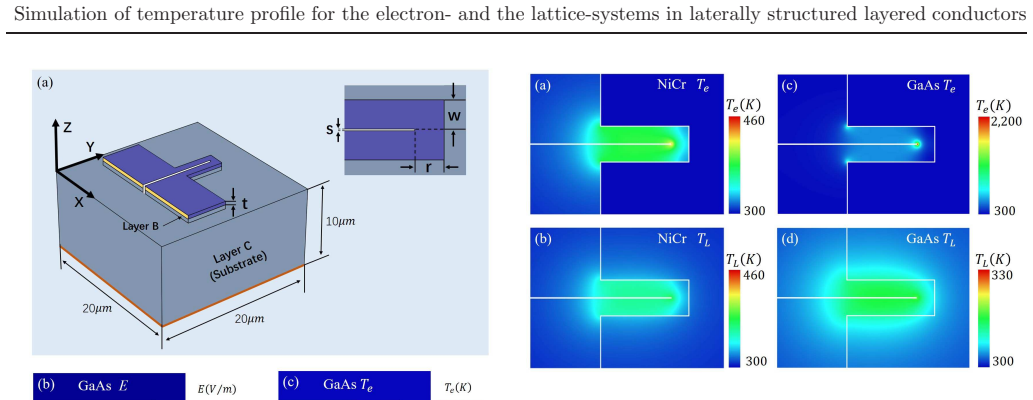
The load-bearing object is the two-sheet model: a conducting layer is divided into an electron sheet (Layer A) and a lattice sheet (Layer B) on a substrate, and the energy lost by electrons to phonons is represented as interface heat flux $P_{e-ph}=(T_e-T_L)C_e/\tau_{e-ph}$, with an effective interface resistance $h_{e-ph}=\tau_{e-ph}/C_e$. Electron heat conduction $\kappa_e$ moves energy within the electron sheet, lattice conduction $\kappa_L$ moves it in the lattice sheet, and a substrate resistance $h_I$ carries it to a 300 K heat sink. The model is solved self-consistently with a finite-element multiphysics solver, which is what turns a geometry with a sharp 15 nm inner corner into a sharply peaked $T_e$ while keeping $T_L$ nearly flat.
What would settle it
Measure the electron temperature profile of a 4.5 V biased U-shaped n-GaAs channel with a nanoscale temperature probe; if the peak $T_e$ is far below about 2000 K or its spatial width is comparable to the lattice hot spot, the two-layer constant-parameter model fails at the corner. Alternatively, running the model with field-dependent $\sigma_e$ from intervalley transfer should reduce the predicted $T_e$; if it does not, the model's temperature dependence is missing.
Extended reading notes
Core claim
The central claim is that a two-layer heat-transport model—one layer for electrons at $T_e$, one for the lattice at $T_L$, coupled by a constant interface resistance $h_{e-ph}=\tau_{e-ph}/C_e$—captures the essential electro-thermal behavior of laterally structured layered conductors. In the n-GaAs U-channel simulated here, Joule heating at the 15 nm inner corner raises $T_e$ to about 2000 K while $T_L$ rises by less than 30 K; in the NiCr lead, $T_e$ and $T_L$ remain essentially equal and the hot spot is much weaker. The paper interprets this semiconductor–metal contrast as coming from the electron specific heat: for the same power input, a semiconductor's electron system has far smaller heat capacity, so electrons are driven far above the lattice. It further argues that high electron mobility is not the reason semiconductors generate hot electrons, since metals conduct better yet stay near equilibrium.
Load-bearing premise
The simulation assumes the electron and lattice subsystems each have a well-defined local temperature and that heat exchange between them is described by a constant interface resistance, even in the tiny corner region where the field is strongest and the carrier distribution may not be thermal.
Editorial extensions
If this is right
- In any semiconductor channel with a sharp bend, the simulation predicts a sharp electron-temperature hot spot at the inner corner, with peak $T_e$ far above $T_L$.
- In metallic leads of the same geometry, the simulation predicts near-equilibrium heating, so hot-electron effects should be absent in metals.
- The quantitative split $(T_e-T_L)=(\tau_{e-ph}/C_e)P$ gives a design rule: reducing $C_e$ or increasing $\tau_{e-ph}$ worsens electron overheating at fixed Joule power.
- Because the model uses only tabulated constants and a conventional solver, it can be applied to arbitrary lateral conductor shapes without Monte Carlo procedures.
- The paper's comparison to the cited experiments implies the model can serve as a first-pass design tool for avoiding hot-electron degradation in real nanoscale devices.
Reading between the lines
- If the specific-heat explanation is right, a semiconductor and a metal with the same electron-phonon relaxation time should still show dramatically different $T_e$–$T_L$ splits at equal Joule power density; this could be tested directly in paired devices.
- The constant-$\sigma_e$ assumption likely fails above the 10 kV/cm field at the corner, where intervalley scattering in GaAs would reduce mobility; a field-dependent version of the model would show whether the 2000 K peak is an upper bound.
- The same two-sheet construction could be extended to transient or pulsed bias, predicting how quickly the electron hot spot forms relative to the lattice, which matters for high-frequency operation.
- A direct experimental check with a nanoscale temperature probe on the same U-shape would test the predicted sharpness of the $T_e$ spike, not just its peak value.
Signed reviews
Editorial analysis
A structured set of objections, weighed in public.
Referee Report
Summary. The manuscript proposes a two-layer electro-thermal model for layered conductors: the conducting sheet is split into an electron sublayer (Layer A) and a lattice sublayer (Layer B) that exchange heat through a lumped interface resistance h_e-ph defined in Eq. (2) as τ_e-ph/C_e. Using COMSOL, the authors simulate a U-shaped n-GaAs channel (35 nm thick, 1 μm wide, 15 nm inner radius, Vb=4.5 V). They report a sharp electron-temperature hotspot with Te reaching ~2000 K at the inner corner while the lattice remains below 330 K. The same calculation for a NiCr lead gives Te≈TL with a ~150 K rise. The paper interprets the semiconductor/metal contrast as arising from the much smaller electron specific heat of GaAs rather than from a difference in electron-phonon coupling, and claims consistency with the experiments of Refs. [32,39].
Significance. If correct, the work offers a simple and computationally convenient strategy for separating electron and lattice temperatures in nanoscale conductors, avoiding full Monte Carlo or Boltzmann simulations. The prediction of a sharp, material-dependent electron-temperature hotspot is falsifiable and could be tested by local thermometry. The model's strength is its transparency: Eq. (5) makes explicit the dependence of the steady-state temperature split on τ_e-ph/C_e times the Joule power. However, the headline quantitative result and the material-contrast interpretation are not yet established, because they rely on constant transport coefficients at the boundary of the validity range stated by the authors themselves, and because the contrast is largely fixed by the input parameters rather than independently derived. For these reasons the paper is promising but needs substantial revision before publication.
major comments (4)
- [Results and discussions, Eq. (5), Table 1] Equation (5) states ΔT_e=(τ_e-ph/C_e)P, and with the Table 1 inputs τ_e-ph=1 ps, C_e=2.3×10^-6 J/(K m^2) for n-GaAs and τ_e-ph=3 ps, C_e=1.1×10^-2 J/(K m^2) for NiCr, the interface resistance h_e-ph differs by a factor of roughly 1600 by construction. The paper's central conclusion that the semiconductor/metal contrast is due to the electron specific heat rather than to the electron-phonon interaction is therefore a restatement of the chosen parameters, not an independent result of the simulation. To make the attribution convincing, the authors should either validate τ_e-ph and C_e independently for both materials or perform controlled variations (for example, changing C_e while keeping τ_e-ph fixed) and show that the simulated contrast tracks the controlled parameter.
- [Simulation model and final paragraph; Fig. 2] The inner-corner field is reported as E≈10 kV/cm with Te≈2000 K, placing the headline result at the upper boundary of the linear-transport regime. In the final paragraph the authors concede that above 10 kV/cm intervalley transfer reduces the mobility, and the values of σ_e, κ_e, and τ_e-ph used in Table 1 are all constants. Because the peak temperature is directly proportional to the local Joule power P=σ_e E^2 and to h_e-ph, the 2000 K number and the material contrast are not yet supported in this regime. The manuscript needs a quantitative estimate of the correction, for example by using a nonlinear velocity-field curve for n-GaAs, or the simulation should be restricted to fields below the threshold where the linear approximation is defensible.
- [Simulation model] The local quasi-equilibrium assumption underlying a single T_e is questionable in the 15 nm corner. With a typical drifted velocity of order 10^7 cm/s and τ_e-ph=1 ps, the electron energy relaxation length is of order 100 nm, comparable to or larger than the geometric feature size, so electrons can carry excess energy away from the hotspot before fully relaxing. The authors should justify the local energy balance or estimate the error from this advection effect; without that, the spatial sharpness of the T_e hotspot cannot be regarded as physical.
- [Simulation model, Eqs. (3)-(4), Table 1] The n-GaAs sheet density N_2D=1.1×10^17 m^-2 gives a Fermi temperature of order 5000 K, so the classical-electron condition k_BT_e ≫ ε_F used to justify Eq. (3) is not satisfied at 300 K and only marginally at 2000 K. The constant C_e=2.3×10^-6 J/(K m^2) used for GaAs should be replaced by the heat capacity of a degenerate or partially degenerate 2D electron gas; at 300 K this is several times smaller, changing the absolute value of T_e in Eq. (5). The qualitative semiconductor/metal contrast is probably unaffected, but the quantitative peak temperature and the parameter table need to be corrected.
minor comments (4)
- [General] There are wording typos in the abstract ('l attice-system') and in the Introduction ('semicodncuctor'); these should be corrected.
- [References] Reference [39] is listed with the same journal, volume, and page as Ref. [34]; its bibliographic data appear incorrect and should be checked.
- [Results and discussions] In the final paragraph the text 'E ≈ 10kV [32]' is missing the '/cm' and should read 'E ≈ 10 kV/cm'.
- [Simulated structure] Details of the COMSOL implementation, such as mesh refinement, convergence criteria, and the resulting total current and dissipated power, are not reported; adding these would improve reproducibility.
Circularity Check
The GaAs/NiCr hot-electron contrast and the ~2000 K GaAs peak are fixed by the assumed tau-e-ph/Ce inputs (Eq. 5 is Eq. 2 rearranged), and the 'validation' cites the authors' own prior experiments from which those inputs were taken.
-
self definitional
[Simulation model, Eqs. (1)-(2); Results and discussions, Eq. (5) and Table 1]
"Pe−ph = (Te − TL)Ce/τe−ph ... he−ph = τe−ph/Ce. ... Te − TL = (τe−ph/Ce)P = he−phP ... For a given P, the rise of Te is proportional to τe−ph, and 1/Ce. ... The specific heat is taken to be Ce = 2.3 × 10⁻⁶ W s/(Km2) and 1.1 × 10⁻² W s/(Km2) ... The electron-phonon energy relaxation time is assumed to be τe−ph = 1 ps and 3ps, respectively for n-GaAs [32] and NiCr [39]."
Eq. (5) is not an independent prediction: it is Eq. (1) rearranged using the definition he−ph = τe−ph/Ce in Eq. (2). The semiconductor/metal contrast is therefore written into Table 1: Ce differs by about four orders of magnitude (2.3e-6 vs 1.1e-2 W s K−1 m−2) while tau differs by only a factor of three (1 vs 3 ps), giving he−ph = 4.3e-7 K m2/W for GaAs and 2.7e-10 K m2/W for NiCr. The abstract's 'interpretation' that the difference is due to electron specific heat is a restatement of these chosen inputs, not a model output that could have come out differently.
-
self citation load bearing
[Simulated structure, parameter choices; Results and discussions, consistency claim]
"The electron-phonon energy relaxation time is assumed to be τe−ph = 1 ps and 3ps, respectively for n-GaAs [32] and NiCr [39]. ... These findings are consistent with recent experimental results reported on metals [39] and semiconductors [32], indicating the validity of the present model."
The load-bearing coefficient he−ph = tau/Ce is attached to Refs. [32] and [39], whose author lists substantially overlap with the present paper (e.g., Komiyama, Yang, An, and Lu; Weng appears in both cited works). The same references are then invoked as the experimental confirmation of the simulation. Because Eq. (5) makes the hot-electron amplitude proportional to these very inputs, the agreement is a closed self-citation loop rather than an independent check. No external, code-verified, or parameter-free benchmark is supplied.
full rationale
The finite-element geometry and heat-conduction problem are genuine: the U-bend field concentration, the spatial extent of the hot spot, and the TL profiles are nontrivial COMSOL solutions, so the paper is not wholly derivational. However, the paper's central physical conclusion—that the semiconductor/metal difference is due to electron specific heat rather than electron-phonon coupling—is directly forced by Eq. (5) and the Table 1 inputs: Delta T = (tau/Ce)P, with he−ph differing by about 1600x between the two materials. The headline Te approximately 2000 K is likewise the output of a fixed tau_e-ph/Ce coefficient in a regime the final paragraph itself flags as nonlinear (constant sigma, kappa, and tau assumed up to E about 10 kV/cm, with the hotspot at that boundary). The consistency claims cite the authors' own prior experiments for the input parameters, so the validation loop is closed by self-citation. Score 6 rather than 8 because the thermal-spatial calculation has independent content and the model is openly presented as based on assumed parameters; score 0-2 is not appropriate because the principal claim reduces to the inputs by construction.
Assumptions & free parameters
free parameters (6)
- tau-e-ph (n-GaAs) =
1 ps
- tau-e-ph (NiCr) =
3 ps
- Ce (n-GaAs) =
2.3e-6 W s/(K m^2)
- Ce (NiCr) =
1.1e-2 W s/(K m^2)
- hI (NiCr) =
3e-8 K m^2/W
- Vb =
4.5 V
assumptions (4)
- standard math Fourier heat conduction and Ohm's law hold in each layer.
- domain assumption Electron and lattice subsystems are in local quasi-equilibrium with well-defined temperatures Te and TL.
- ad hoc to paper Energy exchange between subsystems is described by the lumped interface resistance he-ph = tau-e-ph / Ce (Eq. 2).
- domain assumption All electrical and thermal conductivities are constants independent of temperature and field.
invented entities (1)
-
Electron sublayer (Layer A) and lattice sublayer (Layer B)
Cite this review
Pith. "Pith review of Simulation of temperature profile for the electron- and the lattice-systems in laterally structured layered conductors." pith.science (2026). https://pith.science/paper/CT3DTN4S
@misc{pith2026190802190,
  author       = {Pith},
  title        = {Pith review of: Simulation of temperature profile for the electron- and the lattice-systems in laterally structured layered conductors},
  year         = {2026},
  howpublished = {\url{https://pith.science/paper/CT3DTN4S}},
  note         = {Machine review of arXiv:1908.02190}
}
read the original abstract
Electrons in operating microelectronic semiconductor devices are accelerated by locally varying strong electric field to acquire effective electron temperatures nonuniformly distributing in nanoscales and largely exceeding the temperature of host crystal lattice. The thermal dynamics of electrons and the lattice are hence nontrivial and its understanding at nanoscales is decisively important for gaining higher device performance. Here, we propose and demonstrate that in layered conductors nonequilibrium nature between the electrons and the lattice can be explicitly pursued by simulating the conducting layer by separating it into two physical sheets representing, respectively, the electron- and the lattice-subsystems. We take, as an example of simulating GaAs devices, a 35nm thick 1um wide U-shaped conducting channel with 15nm radius of curvature at the inner corner of the U-shaped bend, and find a remarkable hot spot to develop due to hot electron generation at the inner corner. The hot spot in terms of the electron temperature achieves a significantly higher temperature and is of far sharper spatial distribution when compared to the hot spot in terms of the lattice temperature. Similar simulation calculation made on a metal (NiCr) narrow lead of the similar geometry shows that a hot spot shows up as well at the inner corner, but its strength and the spatial profiles are largely different from those in semiconductor devices. The remarkable difference between the semiconductor and the metal is interpreted to be due to the large difference in the electron specific heat, rather than the difference in the electron phonon interaction. This work will provide useful hints to deeper understanding of the nonequilibrium properties of electrical conductors, through a simple and convenient method for modeling nonequilibrium layered conductors.
Figures


Reference graph
Works this paper leans on
-
[1]
Aninkeviˇcius V., Bareikis V., Katilius R., Liberis J., Matulionien ˙e I., Matulionis A., Sakalas P. and ˇSaltis R. , Phys. Rev. B , 53 (1996) 6893
work page 1996
-
[2]
Matulionis A., Liberis J., Matulioniene I. and Ra- monas M. , Acta Phys. Pol., A , 113 (2008) 967
work page 2008
-
[3]
Levi A. F. J., Hayes J. R., Platzman P. M., Liberis J. and Wiegmann W. , Phys. Rev. Lett. , 55 (1985) 2071
work page 1985
-
[4]
Atar F. B., Aygun L. E., Daglar B., Bayindir M. and Okyay A. K. , Opt. Express, 21 (2013) 7196
work page 2013
-
[5]
Pumarol M. E., Rosamond M. C., Tovee P., Petty M. C., Zeze D. A., F alko V. and Kolosov O. V. , Nano Lett., 12 (2012) 2906
work page 2012
-
[6]
Lan Y.-W., Torres J. C. M., Zhu X., Qasem H., Adle- man J. R., Lerner M. B., Tsai S.-H., Shi Y., Li L.-J., Yeh W.-K. and W ang K. L., Sci. Rep. , 6 (2016) 32503
work page 2016
-
[7]
Guo Z., W an Y., Yang M., Snaider J., Zhu K. and Huang L. , Science, 356 (2017) 59
work page 2017
-
[8]
Lee S., Wijesinghe N., Diaz-Pinto C. and Peng H. , Phys. Rev. B , 82 (2010) 045411
work page 2010
Show all 39 references
-
[9]
and Majima T
Zhang P., Fujitsuka M. and Majima T. , Nanoscale, 9 (2017) 1520
2017
-
[10]
and Cronin S
Li Z., Ezhilarasu G., Chatzakis I., Dhall R., Chen C.-C. and Cronin S. B. , Nano Lett. , 15 (2015) 3977
2015
-
[11]
and P ark J
Lee H., Lee H. and P ark J. Y. , Nano Lett. , 19 (2019) 891
2019
-
[12]
K., Jung C
Lee Y. K., Jung C. H., P ark J., Seo H., Somorjai G. A. and P ark J. Y., Nano Lett. , 11 (2011) 4251
2011
-
[13]
and Li X
Shao W., Yang Q., Zhang C., Wu S. and Li X. , Nanoscale, 11 (2019) 1396
2019
-
[14]
D., Reid A
Konstantinova T., Rameau J. D., Reid A. H., Ab- durazakov O., Wu L., Li R., Shen X., Gu G., Huang Y., Rettig L., A vigo I., Ligges M., Freericks J. K., Kemper A. F., D ¨urr H. A., Bovensiepen U., John- son P. D., W ang X. and Zhu Y. , Sci. Adv. , 4 (2018) eaap7427
2018
-
[15]
Wu K., Chen J., McBride J. R. and Lian T. , Science, 349 (2015) 632
2015
-
[16]
A., Williams K
Tisdale W. A., Williams K. J., Timp B. A., Norris D. J., Aydil E. S. and Zhu X.-Y. , Science, 328 (2010) 1543
2010
-
[17]
and Neogi A
Ashalley E., Gryczynski K., W ang Z., Salamo G. and Neogi A. , Nanoscale, 11 (2019) 3827
2019
-
[18]
and Ventra M
Dubi Y. and Ventra M. Di. , Rev. Mod. Phys., 83 (2011) 131
2011
-
[19]
and Hess O
Hartmann M., Mahler G. and Hess O. , Phys. Rev. Lett., 93 (2004) 080402
2004
-
[20]
and Chrysler G
Mahajan R., Chia-pin C. and Chrysler G. , Proceed- ings of the IEEE , 94 (2006) 1476
2006
-
[21]
L., Halas N
Brongersma M. L., Halas N. J. and Nordlander P. , Nature nanotechnol., 10 (2015) 25
2015
-
[22]
and Tang Z
Peng S., Xing G. and Tang Z. , Nanoscale, 9 (2017) 15612
2017
-
[23]
S., Chavez-Angel E., W agner M
Reparaz J. S., Chavez-Angel E., W agner M. R., Graczykowski B., Gomis-Bresco J., Alzina F. and Torres C. M. S. , Rev. Sci. Instrum. , 85 (2014) 034901
2014
-
[24]
N., Zhan D., Liu L., Suo H., Ni Z
Xu Y. N., Zhan D., Liu L., Suo H., Ni Z. H., Nguyen T. T., Zhao C. and Shen Z. X. , ACS Nano, 5 (2011) 147
2011
-
[25]
Zhang X., Sun D., Li Y., Lee G.-H., Cui X., Chenet D., You Y., Heinz T. F. and Hone J. C. , ACS Appl. Mater. Interfaces , 7 (2015) 25923
2015
-
[26]
and Wickramasinghe H
Nonnenmacher M. and Wickramasinghe H. K. , Appl. Phys. Lett., 61 (1992) 168
1992
-
[27]
H., Briggs G
Harzheim A., Spiece J., Evangeli C., McCann E., F alko V., Sheng Y., W arner J. H., Briggs G. A. D., Mol J. A., Gehring P. and Kolosov O. V. , Nano Lett., 18 (2018) 7719
2018
-
[28]
J., Smithe K
Yalon E., McClellan C. J., Smithe K. K. H., Rojo M. M., Xu R. L., Suryavanshi S. V., Gabourie A. J., Neumann C. M., Xiong F., F arimani A. B. and Pop E., Nano Lett. , 17 (2017) 3429
2017
-
[29]
C., P auly F., Nielaba P., Cuevas J
Cui L., Jeong W., Hur S., Matt M., Klockner J. C., P auly F., Nielaba P., Cuevas J. C., Meyhofer E. and Reddy P. , Science, 355 (2017) 1192
2017
-
[30]
Shi L., Plyasunov S., Bachtold A., McEuen P. L. and Majumdar A. , Appl. Phys. Lett. , 77 (2000) 4295
2000
-
[31]
A., White E
Mecklenburg M., Hubbard W. A., White E. R., Dhall R., Cronin S. B., Aloni S. and Regan B. C. , Science, 347 (2015) 629
2015
-
[32]
and Lu W
Weng Q., Komiyama S., Yang L., An Z., Chen P., Biehs S.-A., Kajihara Y. and Lu W. , Science, 360 (2018) 775
2018
-
[33]
Komiyama S. , J. Appl. Phys. , 125 (2019) 010901
2019
-
[34]
and GOODSON K
SINHA S. and GOODSON K. E. , Int. J. Multiscale Comput. Engineering. , 3 (2005) 107
2005
-
[35]
and Goodnick S.M., Large-Scale Scientific Computing , edited by Lirkov, Ivan and Margenov, Svetozar and W a ´sniewski, Jerzy
V asileska D., Ashok A., Hartin O. and Goodnick S.M., Large-Scale Scientific Computing , edited by Lirkov, Ivan and Margenov, Svetozar and W a ´sniewski, Jerzy. (Springer Berlin Heidelberg) 2010, p. 451-458
2010
-
[36]
and Ka- viany M., ASME 2012 Summer Heat Transfer Conference , 2012 (.)
F an A., Tarau C., Bonner R., P alacios T. and Ka- viany M., ASME 2012 Summer Heat Transfer Conference , 2012 (.)
2012
-
[37]
and P´erez S
Garc´ıa S., ´I˜niguez-de-la-Torre I, Mateos J., Gonz´alez T. and P´erez S. , Semicond. Sci. Technol. , 31 (2016) 065005
2016
-
[38]
and Hao U
W ang Y., Ao J, Liu S. and Hao U. , Appl. Sci. , 9 (2019) 75
2019
-
[39]
and Kajihara Y
Weng Q., Lin K.-T., Yoshida K., Nema H., Komiyama S., Kim S., Hirakaw a K. and Kajihara Y. , Int. J. Multiscale Comput. Engineering. , 3 (2005) 107. p-5
2005
Reviewed August 14, 2026 · model on record in the stance chip above.
Discussion (0). Continue with ORCID to comment.