REVIEW 3 major objections 4 minor 43 references
High-temperature droplet epitaxy of symmetric GaAs/AlGaAs quantum dots
T0 review · 3 major / 4 minor · reviewed 2026-08-14 · deepseek-v4-flash
Pith's one-line read High-temperature droplet epitaxy on GaAs(111)A can produce symmetric, optically clean quantum dots by balancing arsenization inside the droplet against gallium diffusion outside it.
desk verdict The high-temperature droplet epitaxy recipe is a real experimental advance for symmetric GaAs QDs on (111)A, but the one-parameter kinetic model in Eq. (3) does not survive contact with the paper's own pressure-series data. read the letter →
The pith
A machine-rendered reading of the paper's core claim, the machinery that carries it, and where it could break.
The reading
What carries the argument
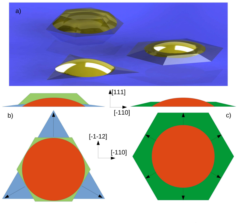
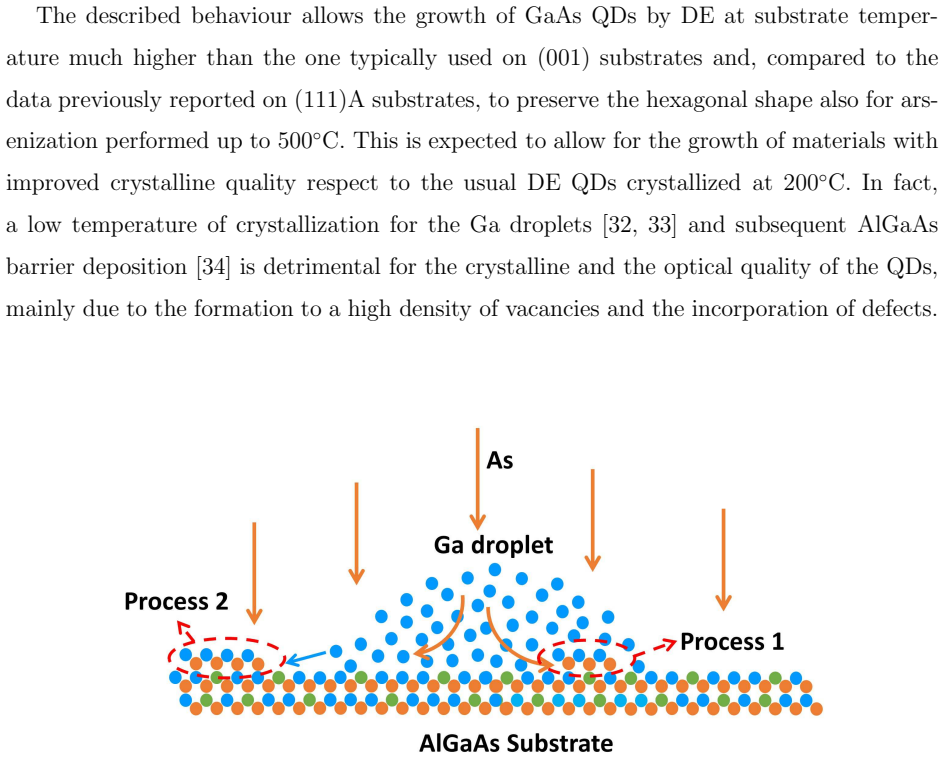
The load-bearing quantity is the ratio γ = V1/V, together with its model equation γ(J_As, T) = [1 + C exp(-E_D/kT)/J_As]^-1, where C collects the arsenic residence time, the diffusion prefactor, and geometric constants. This ratio encodes the competition between process 1, arsenic-driven crystallization inside the droplet, and process 2, gallium detachment, diffusion, and incorporation on the surrounding surface: γ near 1 means three-dimensional island growth, while γ near 0 means the droplet feeds a flat two-dimensional layer. The identity that makes the mechanism work is that the process-2 growth rate is independent of arsenic flux once the gallium diffusion length squared scales as 1/J_As, so raising the arsenic flux shifts the balance back toward process 1. Shape enters separately: high arsenic flux equalizes the incorporation velocities at A steps and B steps, turning the triangular high-temperature shape back into a regular hexagon.
What would settle it
Measure γ from AFM at 500 °C for a dense series of arsenic beam equivalent pressures from below 1×$10^{-7}$ to above 1×$10^{-4}$ Torr and test the model's prediction that 1/γ = 1 + C/J_As with a single constant C. A systematic departure from this linear-in-1/J_As form at low flux, or a saturation of γ with increasing flux, would falsify the claim that gallium diffusion scales as 1/J_As on (111)A.
Extended reading notes
Core claim
The paper establishes that droplet epitaxy on GaAs(111)A can be performed at substrate temperatures near 500 °C and still produce GaAs/AlGaAs quantum dots with regular hexagonal shape and high crystalline quality, provided the arsenic beam equivalent pressure during arsenization is raised to about 5×$10^{-5}$ Torr. The mechanism is a kinetic balance between two processes: arsenic dissolving into the liquid gallium droplet and crystallizing GaAs inside its footprint, versus gallium atoms detaching from the droplet, diffusing across the surface, and incorporating elsewhere. The ratio γ = V1/V between the final dot volume and the GaAs volume available from the droplet quantifies this balance, and a one-parameter model fits the measured dependence of γ on substrate temperature and arsenic flux. According to the model, the short residence time of arsenic on the (111)A surface keeps the inside-droplet crystallization dominant even at high temperature, while the high arsenic flux equalizes incorporation at A and B steps and restores the symmetric hexagon. Capped dots from this recipe emit with a mean neutral-exciton linewidth of about 15 µeV and a mean fine-structure splitting of about 4.5 µeV.
Load-bearing premise
The model assumes that gallium diffusion and incorporation on GaAs(111)A follow the same physics as on GaAs(001), in particular that the gallium diffusion length squared is inversely proportional to the arsenic flux; if that scaling does not hold on the (111)A surface, the predicted rise of γ with arsenic flux and the explanation of the high-temperature series lose their basis.
Editorial extensions
If this is right
- Crystallization of the dots and deposition of the AlGaAs capping layer can both be done near 500 °C, avoiding the low-temperature defect incorporation that limits standard droplet epitaxy.
- The arsenic flux becomes a direct shape-control knob: low flux at high temperature produces triangular dots by suppressing B-step incorporation, while about 5×10^-5 Torr restores regular hexagonal dots.
- The capped dots emit in the 700–765 nm range with narrow ensemble lines, mean fine-structure splitting of about 4.5 µeV, and best neutral-exciton linewidth of 9 µeV, the properties needed for high-fidelity entangled-photon emission.
- The one-parameter model predicts a quantitative relation between crystallized volume fraction, arsenic flux, and temperature that can be used to design dot size and density for wavelength-specific applications.
Reading between the lines
- Beyond the paper, the same kinetic balance should be testable with As2 instead of As4 or on other (111)A III-V surfaces; if the arsenic-residence-time argument is right, the flux needed to restore hexagonal symmetry will shift in a predictable way.
- A design rule implicit in the model is to choose temperature and arsenic flux so that γ stays high and the A/B step incorporation ratio approaches one; partial-arsenization quench series followed by atomic force microscopy could map this rule directly.
- Although the paper reports emission in the 700–765 nm range, the same recipe could plausibly be tuned to the rubidium D2 line near 780 nm by adjusting dot height, a testable extension for the hybrid quantum-network application cited in the paper.
Signed reviews
Editorial analysis
A structured set of objections, weighed in public.
Referee Report
Summary. The manuscript reports a high-temperature droplet epitaxy procedure for fabricating symmetric GaAs/AlGaAs quantum dots on GaAs(111)A substrates. Droplets of liquid Ga are formed at 450 °C and then arsenized at temperatures up to 500 °C with As beam equivalent pressures up to 7×10⁻⁵ Torr. Atomic force microscopy shows that at 500 °C and high As flux the dots are symmetric hexagonal truncated pyramids, whereas at lower flux they are triangular, and at 200 °C they are hexagonal with steeper sidewalls. The measured GaAs volume inside the dots is used to define γ = V₁/V, the fraction of the available Ga crystallized in the three-dimensional dot as opposed to incorporated into the surrounding surface. The paper proposes a two-process model: arsenic incorporation at the droplet base (process 1) and Ga detachment, diffusion, and incorporation on the surface (process 2). Equation (3) gives γ as a function of As flux and temperature with one fitted parameter, and the authors report that the data are 'nicely reproduced.' The optical properties of capped dots are characterized by ensemble photoluminescence; the high-temperature dots show small blue-shift upon capping, attributed to reduced interdiffusion, and the authors cite their prior work [22] for narrow linewidths and low fine-structure splitting.
Significance. If the empirical findings hold, the paper makes a useful contribution to droplet epitaxy for quantum photonics: it demonstrates a route to fabricate symmetric GaAs/AlGaAs quantum dots on (111)A at temperatures about 300 °C higher than conventional droplet epitaxy, with reduced defect densities and preserved hexagonal symmetry. The AFM data directly support the main morphological trends versus temperature and As flux, and the proposed model is falsifiable and uses a single fitted parameter, which is a methodological strength. The optical quality claims, however, rely on the previously published measurements in Ref. [22] rather than on new optical data presented here. The quantitative model is not fully supported by the pressure-series data, so the mechanistic interpretation should be treated as provisional pending revision.
major comments (3)
- [Section IV, Eq. (3) and Figure 4] The model in Eq. (3) systematically overpredicts the As-pressure-series data that it is claimed to reproduce. With the stated fit constant μζRD₀/ρD = 2×10² Torr, E_D = 1.06 eV, and T = 500 °C, the model predicts γ(H₄)/γ(H₁) ≈ 9.0, γ(H₅)/γ(H₁) ≈ 9.9, and γ(H₃)/γ(H₁) ≈ 6.0. Since the deposited Ga amount and hence V are identical for all H-series samples, the corresponding measured ratios from Table I are 5.4, 5.6, and 3.3, respectively. The model also cannot describe the saturation of γ at approximately 0.45 for H₄ and H₅, because Eq. (3) increases monotonically toward 1. The paper mentions 'limited As solubility and diffusivity in the droplet' only qualitatively; this saturation mechanism must be included in the model, or the quantitative claim that the data are 'nicely reproduced' must be withdrawn.
- [Section IV, Eq. (2)] The derivation of Eq. (2) assumes that the diffusion/incorporation process on GaAs(111)A 'follows the same physics' as on GaAs(001), specifically that ℓ² ∝ 1/J_As. This assumption is not independently tested for the (111)A surface, and it is the reason the process-2 rate becomes independent of J_As in Eq. (2), so the predicted dependence of γ on As flux rests on an unverified universality. The authors should either provide a direct test of this scaling on (111)A, for example from a dedicated diffusion-length measurement, or explicitly reframe the model as a heuristic whose pressure dependence is not yet established.
- [Figure 4 and Table I] The experimental values of γ are presented without uncertainty estimates, although the AFM-derived volumes in Table I show scatter and the dot dimensions have reported standard deviations. Without error bars or a quantitative propagation of the AFM uncertainties, it is not possible to assess whether the discrepancy between the model and the H₄/H₅ data is significant. The paper's central quantitative claim requires at least representative uncertainty bars on the volume measurements.
minor comments (4)
- [Section IV, first paragraph] The phrase 'To understand the reasons beyond the observed behavior' should read 'To understand the reasons behind the observed behavior.'
- [Figure 4 caption] The caption states that the continuous line 'reports the fit of the data using Eq. (3),' but the line for the pressure series is a prediction computed with a parameter fitted to the temperature series, not a fit to the pressure data. Please clarify this distinction in the caption.
- [Table I caption] The caption 'Substrate temperature and Ga flux of fabricated samples for the droplet formation' is confusing because the table lists the substrate temperature during Ga deposition, the Ga amount, the temperature and As BEP during arsenization, and the resulting volume. Please reword to describe the columns accurately.
- [Section III] The text says that the measured GaAs volume is 'always lower from the expected volume,' which should be 'always lower than the expected volume.'
Circularity Check
No definitional circularity: Eq. (3) follows from an explicit two-process mass balance with one fitted kinetic constant, and the optical-quality assertions rest on separately published measurements.
full rationale
The derivation chain is not circular. Section IV defines the two crystallization channels (droplet interior, Eq. (1); out-of-droplet diffusion/incorporation, Eq. (2)) and combines them through the Ga conservation condition V = V1(τ) + V2(τ) to obtain Eq. (3), γ = [1 + (μζRD0/ρD) exp(−ED/kT)/JAs]^{-1}. The cancellation that makes V2 independent of JAs is explicit algebra using ℓ² ∝ 1/JAs, not a restatement of the target γ. The single constant μζRD0/ρD is fitted to the temperature series (L1, M1, H1), and the same curve is then compared with the As-flux series; this is a one-parameter consistency check, not a fitted input renamed as a prediction. The (001)-surface diffusion scaling and the (111)A activation energy are adopted from prior work with stated physical content, and the paper openly assumes the same physics applies on (111)A; an assumption of transferability is not definitional circularity. The optical-quality claim in the Conclusions cites the separately published measurements in [22]; a self-citation to published data is real evidence, and the current paper adds its own AFM and ensemble-PL characterization. The manuscript also flags the saturation limit for very high As flux ('The upper limit for this effect is marked by the limited As solubility and diffusivity in the droplet for extremely high As flux'), which is a scope/correctness limitation—the model indeed tends to overpredict the H4→H5 plateau—but that is falsifiability, not circularity.
Assumptions & free parameters
free parameters (1)
- µζRD0/ρD =
2x10^2 Torr
assumptions (4)
- domain assumption Diffusion and incorporation of Ga adatoms on GaAs(111)A follows the same physics as on GaAs(001), including the scaling ℓ^2 = D0 exp(-ED/kT)(Nd/JAs).
- domain assumption The crystallization rate inside the droplet is linear in time with constant ρD, assuming slow variation of the liquid-solid interface area.
- domain assumption All deposited gallium is collected in the droplets, so the initial droplet volume equals the total gallium volume.
- standard math The total crystallized GaAs volume equals the sum of process 1 and process 2 volumes when the droplet is fully consumed.
Cite this review
Pith. "Pith review of High-temperature droplet epitaxy of symmetric GaAs/AlGaAs quantum dots." pith.science (2026). https://pith.science/paper/UNPIP2C5
@misc{pith2026190802506,
  author       = {Pith},
  title        = {Pith review of: High-temperature droplet epitaxy of symmetric GaAs/AlGaAs quantum dots},
  year         = {2026},
  howpublished = {\url{https://pith.science/paper/UNPIP2C5}},
  note         = {Machine review of arXiv:1908.02506}
}
read the original abstract
We introduce a high-temperature droplet epitaxy procedure, based on the control of the arsenization dynamics of nanoscale droplets of liquid Ga on GaAs(111)A surfaces. The use of high temperatures for the self-assembly of droplet epitaxy quantum dots solves major issues related to material defects, introduced during the droplet epitaxy fabrication process, which limited its use for single and entangled photon sources for quantum photonics applications. We identify the region in the parameter space which allows quantum dots to self-assemble with the desired emission wavelength and highly symmetric shape while maintaining a high optical quality. The role of the growth parameters during the droplet arsenization is discussed and modelled.
Figures

Figures from the paper (2 more)


Reference graph
Works this paper leans on
-
[22]
Francesco Basso Basset, Sergio Bietti, Marcus Reindl, Luca Esposito, Alexey Fedorov, Daniel Huber, Armando Rastelli, Emiliano Bonera, Rinaldo Trotta, and Stefano Sanguinetti. High- Yield Fabrication of Entangled Photon Emitters for Hybrid Q uantum Networking Using High- 16 Temperature Droplet Epitaxy. Nano Letters , 18:505, 2018
work page 2018
-
[1]
H.J. Kimble. The quantum internet. Nature, 453(7198):1023–1030, 2008. cited By 1631
work page 2008
-
[2]
Recent advances on in tegrated quantum communications
Adeline Orieux and Eleni Diamanti. Recent advances on in tegrated quantum communications. Journal of Optics , 18(8):083002, 2016
work page 2016
-
[3]
Ladd, Fedor Jelezko, Raymond Laflamme, Yasun obu Nakamura, Christopher R
Thaddeus D. Ladd, Fedor Jelezko, Raymond Laflamme, Yasun obu Nakamura, Christopher R. Monroe, and Jeremy Lloyd O’Brien. Quantum computers. Nature, 464:45–53, 2010
work page 2010
-
[4]
Quantum computers ready to leap ou t of the lab in 2017
Davide Castelvecchi. Quantum computers ready to leap ou t of the lab in 2017. Nature, 541:9–10, 2017
work page 2017
-
[5]
Munro, Koji Azuma, Kiyoshi Tamaki, and Kae Nem oto
William J. Munro, Koji Azuma, Kiyoshi Tamaki, and Kae Nem oto. Inside quantum repeaters. IEEE Journal of Selected Topics in Quantum Electronics , 21:78–90, 2015
work page 2015
-
[6]
Qua ntum internet: A vision for the road ahead
Stephanie Wehner, David Elkouss, and Ronald Hanson. Qua ntum internet: A vision for the road ahead. Science, 362(6412), 2018
work page 2018
-
[7]
Droplet epitaxy of semiconductor nanostructures for quant um photonic devices
Massimo Gurioli, Zhiming Wang, Armando Rastelli, Takas hi Kuroda, and Stefano Sanguinetti. Droplet epitaxy of semiconductor nanostructures for quant um photonic devices. Nature Ma- terials, 2019
work page 2019
Show all 43 references
-
[8]
Fabrication of GaAs Quan- tum Dots by Modified Droplet Epitaxy
Katsuyuki Watanabe, Nobuyuki Koguchi, and Yoshihiko Go toh. Fabrication of GaAs Quan- tum Dots by Modified Droplet Epitaxy. Japanese Journal of Applied Physics , 39(2):L79–L81, 2000
2000
-
[9]
Nanometer-scale GaA s ring structure grown by droplet epitaxy
Takaaki Mano and Nobuyuki Koguchi. Nanometer-scale GaA s ring structure grown by droplet epitaxy. Journal of Crystal Growth , 278(1-4):108–112, may 2005
2005
-
[10]
Fabrication of multiple concentric nanoring structures
Claudio Somaschini, Sergio Bietti, Nobuyuki Koguchi, and Stefano Sanguinetti. Fabrication of multiple concentric nanoring structures. Nano Letters, 9(10):3419–3424, oct 2009
2009
-
[11]
Shape control via surface reconstruction kinetics of droplet epitaxy nan ostructures
Claudio Somaschini, Sergio Bietti, Nobuyuki Koguchi, and Stefano Sanguinetti. Shape control via surface reconstruction kinetics of droplet epitaxy nan ostructures. Applied Physics Letters , 97(20):203109, 2010
2010
-
[12]
Droplet epi- taxial growth of highly symmetric quantum dots emitting at t elecommunication wavelengths on InP(111)A
Neul Ha, Xiangming Liu, Takaaki Mano, Takashi Kuroda, K azutaka Mitsuishi, Andrea Castel- lano, Stefano Sanguinetti, Takeshi Noda, Yoshiki Sakuma, a nd Kazuaki Sakoda. Droplet epi- taxial growth of highly symmetric quantum dots emitting at t elecommunication wavelengths on InP...
2014
-
[13]
Nanowire quantum dots as an ideal source of entangled 15 photon pairs
Ranber Singh and Gabriel Bester. Nanowire quantum dots as an ideal source of entangled 15 photon pairs. Phys. Rev. Lett. , 103:063601, Aug 2009
2009
-
[14]
In(ga)as/gaas quantum dots grown on a (111) surface as ideal sources of entangled photon pairs
Andrei Schliwa, Momme Winkelnkemper, Anatol Lochmann , Erik Stock, and Dieter Bimberg. In(ga)as/gaas quantum dots grown on a (111) surface as ideal sources of entangled photon pairs. Phys. Rev. B , 80:161307, Oct 2009
2009
-
[15]
Self-limiting growth of hexagonal and triangular q uantum dots on (111)A
Masafumi Jo, Takaaki Mano, Marco Abbarchi, Takashi Kur oda, Yoshiki Sakuma, and Kazuaki Sakoda. Self-limiting growth of hexagonal and triangular q uantum dots on (111)A. Crystal Growth and Design , 12(111):1411–1415, 2012
2012
-
[16]
Yamaguchi, M
H. Yamaguchi, M. R. Fahy, and B. a. Joyce. Inhibitions of three dimensional island formation in InAs films grown on GaAs (111)A surface by molecular beam ep itaxy. Applied Physics Letters, 69(6):776, 1996
1996
-
[17]
Symmetric quantum dots as e fficient sources of highly entangled photons: Violation of bell’s inequality without spectral and temporal filtering
Takashi Kuroda, Takaaki Mano, Neul Ha, Hideaki Nakajim a, Hidekazu Kumano, Bernhard Urbaszek, Masafumi Jo, Marco Abbarchi, Yoshiki Sakuma, Kaz uaki Sakoda, Ikuo Suemune, Xavier Marie, and Thierry Amand. Symmetric quantum dots as e fficient sources of highly entangled photons: Vi...
2013
-
[18]
Seguin, A
R. Seguin, A. Schliwa, S. Rodt, K. P¨ otschke, U. W. Pohl, and D. Bimberg. Size-dependent fine- structure splitting in self-organized InAs / GaAs quantum dots. Phys. Rev. Lett. , 95:257402, Dec 2005
2005
-
[19]
J. Treu, C. Schneider, A. Huggenberger, T. Braun, S. Rei tzenstein, S. Hfling, and M. Kamp. Substrate orientation dependent fine structure splitting o f symmetric in(ga)as/gaas quantum dots. Applied Physics Letters , 101(2):022102, 2012
2012
-
[20]
M ereni, Agnieszka Gocalinska, and Emanuele Pelucchi
Gediminas Juska, Valeria Dimastrodonato, Lorenzo O. M ereni, Agnieszka Gocalinska, and Emanuele Pelucchi. Towards quantum-dot arrays of entangle d photon emitters. Nature Pho- tonics, 7:527 EP –, May 2013
2013
-
[21]
Yerino, Paul J
Christopher D. Yerino, Paul J. Simmonds, Baolai Liang, Daehwan Jung, Christian Schneider, Sebastian Unsleber, Minh Vo, Diana L. Huffaker, Sven H¨ ofling, Martin Kamp, and Minjoo Lawrence Lee. Strain-driven growth of gaas(111) quantum do ts with low fine structure split- ting. App...
2014
-
[23]
Akopian, L
N. Akopian, L. Wang, A. Rastelli, O. G. Schmidt, and V. Zw iller. Hybrid semiconductor- atomic interface: slowing down single photons from a quantu m dot. Nature Photonics , 5:230 EP –, Feb 2011
2011
-
[24]
Self-assembly of symme tric GaAs quantum dots on (111)A substrates: Suppression of fine-structure splitt ing
Takaaki Mano, Marco Abbarchi, Takashi Kuroda, Brian Mc skimming, Akihiro Ohtake, Kazu- taka Mitsuishi, and Kazuaki Sakoda. Self-assembly of symme tric GaAs quantum dots on (111)A substrates: Suppression of fine-structure splitt ing. Applied Physics Express , 3(6):065203, may 2010
2010
-
[25]
Unstrai ned GaAs quantum dashes grown on GaAs(001) substrates by droplet epitaxy
Masafumi Jo, Takaaki Mano, and Kazuaki Sakoda. Unstrai ned GaAs quantum dashes grown on GaAs(001) substrates by droplet epitaxy. Applied Physics Express , 3(4):045502, apr 2010
2010
-
[26]
Fedorov, Nobuyu ki Koguchi, and Stefano Sanguinetti
Claudio Somaschini, Sergio Bietti, a. Fedorov, Nobuyu ki Koguchi, and Stefano Sanguinetti. Concentric Multiple Rings by Droplet Epitaxy: Fabrication and Study of the Morphological Anisotropy. Nanoscale Research Letters, 5:1865–1867, aug 2010
2010
-
[27]
Annealing induced anisotropy in GaAs/AlGaAs quantum dots grown by droplet epitaxy
Silvia Adorno, Sergio Bietti, and Stefano Sanguinetti . Annealing induced anisotropy in GaAs/AlGaAs quantum dots grown by droplet epitaxy. Journal of Crystal Growth , 378:515– 518, sep 2013
2013
-
[28]
Wang, Kyland Holmes, Yuriy I
Zhiming M. Wang, Kyland Holmes, Yuriy I. Mazur, Kimberl y A. Ramsey, and Gre- gory J. Salamo. Self-organization of quantum-dot pairs by h igh-temperature droplet epitaxy. Nanoscale Research Letters, 1(1):57, Jul 2006
2006
-
[29]
Ehrlich-Schwoebel Effect on the Growth Dynamics of GaAs(111) A surfaces
Luca Esposito, Sergio Bietti, Alexey Fedorov, Richard Noetzel, and Stefano Sanguinetti. Ehrlich-Schwoebel Effect on the Growth Dynamics of GaAs(111) A surfaces. PHYSICAL REVIEW MATERIALS , 1:024602, 2017
2017
-
[30]
Surface structures of GaAs {111}A,B-(22)
Akihiro Ohtake, Jun Nakamura, Takuji Komura, Takashi H anada, Takafumi Yao, Hiromi Kuramochi, and Masashi Ozeki. Surface structures of GaAs {111}A,B-(22). Physical Review B, 64(4):045318, jun 2001
2001
-
[31]
Al-Ga monolayer lateral growth observed in situ by scanning electron microscopy
Kiyoshi Kanisawa, Jiro Osaka, Shigeru Hirono, and Naoh isa Inoue. Al-Ga monolayer lateral growth observed in situ by scanning electron microscopy. Applied Physics Letters, 58(21):2363– 2365, 1991
1991
-
[32]
Minami, Y
Stefano Sanguinetti, Katsuyuki Watanabe, Takashi Kur oda, F. Minami, Y. Gotoh, and Nobuyuki Koguchi. Effects of post-growth annealing on the opt ical properties of self-assembled GaAs/AlGaAs quantum dots. Journal of Crystal Growth , 242:321–331, 2002. 17
2002
-
[33]
Gerosa, Claudio Somaschini, Sergio Bietti, Nobuyuki Koguchi, E
Stefano Sanguinetti, Takaaki Mano, a. Gerosa, Claudio Somaschini, Sergio Bietti, Nobuyuki Koguchi, E. Grilli, M. Guzzi, Massimo Gurioli, and Marco Abb archi. Rapid thermal anneal- ing effects on self-assembled quantum dot and quantum ring str uctures. Journal of Applied Physics...
2008
-
[34]
Distribution of exciton emiss ion linewidth observed for GaAs quantum dots grown by droplet epitaxy
Keiji Kuroda, Takashi Kuroda, Katsuyuki Watanabe, Tak aaki Mano, Giyuu Kido, Nobuyuki Koguchi, and Kazuaki Sakoda. Distribution of exciton emiss ion linewidth observed for GaAs quantum dots grown by droplet epitaxy. Journal of Luminescence , 130(12):2390–2393, 2010
2010
-
[35]
Scaccabarozzi, E
Claudio Somaschini, Sergio Bietti, a. Scaccabarozzi, E. Grilli, and Stefano Sanguinetti. Self- assembly of quantum dot-disk nanostructures via growth kin etics control. Crystal Growth and Design, 12(3):1180–1184, mar 2012
2012
-
[36]
Gallium surface diffusion on GaAs (001) surfaces measured by c rystallization dynamics of Ga droplets
Sergio Bietti, Claudio Somaschini, Luca Esposito, Ale xey Fedorov, and Stefano Sanguinetti. Gallium surface diffusion on GaAs (001) surfaces measured by c rystallization dynamics of Ga droplets. Journal of Applied Physics , 116(11):114311, sep 2014
2014
-
[37]
Characterization and Effect of Thermal Anneali ng on InAs Quantum Dots Grown by Droplet Epitaxy on GaAs(111)A Substrates
Sergio Bietti, Luca Esposito, Alexey Fedorov, Andrea B allabio, Andrea Martinelli, and Stefano Sanguinetti. Characterization and Effect of Thermal Anneali ng on InAs Quantum Dots Grown by Droplet Epitaxy on GaAs(111)A Substrates. Nanoscale Research Letters, 10(1):247, 2015
2015
-
[38]
Tersoff, and David E Jesson
Z Y Zhou, C X Zheng, W X Tang, J. Tersoff, and David E Jesson. O rigin of Quantum Ring Formation During Droplet Epitaxy. Physical Review Letters , 111(3):036102, jul 2013
2013
-
[39]
J. N. Shapiro, A. Lin, D. L. Huffaker, and C. Ratsch. Potent ial energy surface of in and Ga adatoms above the (111)A and (110) surfaces of a GaAs nanop illar. Physical Review B - Condensed Matter and Materials Physics , 84(8):1–5, 2011
2011
-
[40]
Sato, K.; Fahy
M.; Joyce B. Sato, K.; Fahy. Reflection high energy elect ron diffraction intensity oscillation study of the growth of gaas on gaas(111)a. Surface Science, 315:105–111, 1994
1994
-
[41]
Bastard J
G. Bastard J. Y. Marzin. CALCULATION OF THE ENERGY LEVEL S IN InAs/GaAs QUANTUM DOTS. Solid state communications , 92(5):437–442, 1994
1994
-
[42]
Ochiai, Stefano Sangu inetti, K
Takashi Kuroda, Takaaki Mano, T. Ochiai, Stefano Sangu inetti, K. Sakoda, G. Kido, and Nobuyuki Koguchi. Optical transitions in quantum ring comp lexes. Physical Review B , 72(20):8, nov 2005
2005
-
[43]
Pavesi and M
L. Pavesi and M. Guzzi. Photoluminescence of AI$ {x}$Ga$ {1-x}$As alloys. Journal of Applied Physics , 75(10):4779, 1994. 18
1994
Reviewed August 14, 2026 · model on record in the stance chip above.
Discussion (0). Continue with ORCID to comment.