REVIEW 2 major objections 7 minor 54 references
Disordered Quantum Transport in Quantum Anomalous Hall Insulator-Superconductor Junctions
T0 review · 2 major / 7 minor · reviewed 2026-08-14 · deepseek-v4-flash
Pith's one-line read This paper claims that disorder leaves the zero-bias transmission of a single chiral edge mode through a quantum anomalous Hall/superconductor junction at unity, while multiple edge modes or coexisting metallic modes make the transmission…
desk verdict Disorder-averaged transport in QAH/SC junctions is a genuinely useful addition, but the zero-bias robustness for a single chiral mode is only proven for chemical-potential disorder. read the letter →
The pith
A machine-rendered reading of the paper's core claim, the machinery that carries it, and where it could break.
The reading
What carries the argument
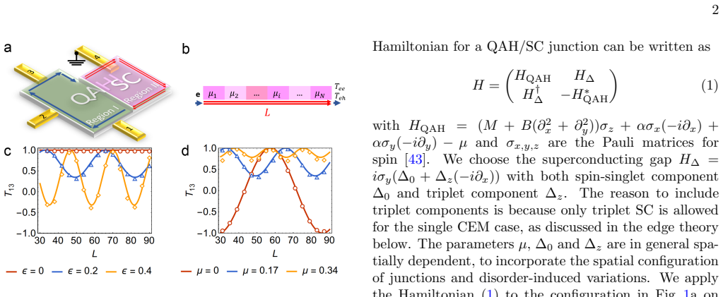
The analysis is carried by the effective edge Hamiltonian $H_{\mathrm{eff}}$ for the chiral edge modes, with only a p-wave (linear-in-$k$) pairing term; in the single-mode basis particle-hole symmetry forbids a constant s-wave pairing term, so the Hamiltonian reads $H_{\mathrm{eff}} = (v_f k - \mu)\tau_z - v_\Delta k \tau_x$ in the electron-hole basis. This linear pairing is what makes the zero-energy transmission exactly one, because at $\epsilon = 0$ the two eigenvectors of the transfer matrix acquire equal phase and no particle-hole conversion develops. Disorder is modeled as independent random local chemical potentials distributed uniformly on $[-\mu_{\mathrm{imp}}/2, \mu_{\mathrm{imp}}/2]$, and the quoted transmission is the ensemble average over many such configurations.
What would settle it
Numerically simulate the lattice QAH/SC junction with disorder applied to the pairing order parameter as well as to the chemical potential (e.g., random on-site $\Delta_0$ with zero mean), and compute $T_{13}$ at $\epsilon=0$ for a junction many times the elastic mean free path; if $\bar{T}_{13}$ decays exponentially with $L$, the single-mode p-wave protection is not robust to pairing disorder, and an experimental probe would be a zero-bias two-terminal conductance of $e^2/2h$ rather than $e^2/h$ in the single-mode limit.
Extended reading notes
Core claim
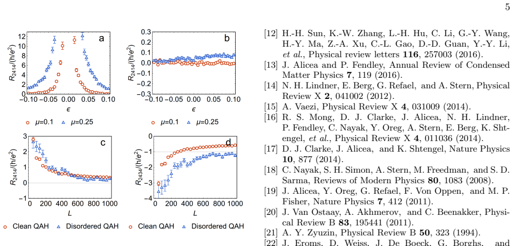
The central claim, stated on the paper's own terms, is that the diffusive transport regime of a QAH/SC junction is controlled by the number and character of the conducting channels. In the single chiral edge mode case, the effective edge Hamiltonian contains only a p-wave (linear-in-momentum) pairing term, and this is the reason that the electron-electron transmission $T_{ee}$ stays at one while the Andreev-conversion transmission $T_{eh}$ stays at zero as the incident energy $\epsilon$ approaches zero. Disorder, modeled as random local chemical potentials, does not change that zero-bias result because the p-wave pairing term has no $k$-independent component to scatter the electron-hole pair at zero energy. For multiple chiral modes, or for a chiral mode coexisting with a non-chiral metallic mode, an $s$-wave pairing component between different modes appears, and disorder then dephases the electron-hole oscillations, so the averaged transmission $\bar{T}_{13}$ decays exponentially with length and the junction acts as a half-electron half-hole converter. The paper further shows that the four-terminal resistances satisfy $R_{24,14}+R_{24,34}=-h/e^2$ for one chiral mode and for the fully disordered coexisting case, and $-h/2e^2$ for two chiral modes, providing a measurable fingerprint of the transport regime.
Load-bearing premise
The load-bearing premise is that disorder in the junction only changes the local chemical potential and never generates a constant s-wave pairing term in the edge-mode basis; if interface roughness couples to the pairing field itself, the p-wave-only protection of the zero-bias transmission collapses.
Editorial extensions
If this is right
- In the single chiral edge mode case, the zero-bias transmission $T_{13}$ stays at 1 even when the elastic scattering length is much shorter than the junction, so Andreev conversion is completely suppressed at zero bias.
- Away from zero bias, disorder makes $\bar{T}_{13}$ decay exponentially with junction length, with a decay length that grows as energy goes to zero, so finite-bias measurements lose the protection.
- When two chiral modes are present, $\bar{T}_{13}$ decays exponentially and saturates near zero for long junctions, so the outgoing current becomes half electrons and half holes.
- When a chiral mode coexists with a non-chiral metallic mode and the QAH region is disordered, the helical mode Anderson-localizes but still mediates Andreev conversion, so $\bar{T}_{13}$ decays to zero even at zero energy.
- The resistance combinations $R_{24,14}+R_{24,34}$ equal $-h/e^2$ for one CEM and $-h/2e^2$ for two CEMs, giving a measurable distinction between the regimes.
Reading between the lines
- A natural extension is to let disorder act on the pairing term as well as the chemical potential; if interface roughness generates an s-wave component in the edge basis, the zero-bias plateau in the single-mode case should disappear, and the paper's central contrast would be weakened.
- The exponential decay in the multi-mode case suggests that the crossover from clean oscillatory conductance to the diffusive half-electron/half-hole limit could be used as a length-dependent diagnostic of how many transport channels actually reach a superconducting contact.
- The resistance sum rule offers a practical channel-counting probe that could be checked on existing QAH/SC devices before attempting Majorana interpretation of conductance kinks.
Signed reviews
Editorial analysis
A structured set of objections, weighed in public.
Referee Report
Summary. The paper studies disordered quantum transport through a planar junction between a quantum anomalous Hall insulator and a superconductor, using effective edge models. For a single chiral edge mode (CEM), described by a k-linear p-wave pairing Hamiltonian, the authors derive an analytic transmission formula T13(ε,L) and validate it against numerical transport simulations of a full BdG lattice model in the clean limit. They then add on-site chemical-potential disorder along the junction and find that the zero-energy transmission stays at unity, so the four-terminal resistance diverges at zero bias. In contrast, for two CEMs or a CEM coexisting with non-chiral metallic modes, disorder causes the averaged transmission to decay exponentially with junction length, giving equal electron and hole transmission; the authors propose resistance sum rules R24,14+R24,34 = −h/e², −h/2e², or a non-quantized value to distinguish the four physical cases.
Significance. If the central results hold, the paper makes a useful contribution to the ongoing debate about the e2/2h conductance kink attributed to chiral Majorana modes. It provides concrete, falsifiable signatures: the zero-bias resistance divergence for a single CEM, the exponential decay and half-electron/half-hole conversion for multiple or non-chiral modes, and resistance sum rules that distinguish the cases. The clean-limit analytic formula (Eq. 3) is a strength, as it is checked against full-model numerics, and the disorder-averaged results use a stated number of configurations with standard errors. The main uncertainties are the restricted disorder model and the sign convention of the proposed sum rules; both are addressable.
major comments (2)
- [Model Hamiltonian and Transport of a single CEM (Eq. (2), Fig. 2, Appendix B)] The zero-bias robustness result for the single CEM is established only against on-site chemical-potential disorder μ_i in the effective edge Hamiltonian (2), although Eq. (1) states that μ, Δ0, and Δz are all in principle spatially dependent to incorporate disorder-induced variations. The particle-hole symmetry argument in Appendix B rules out a constant singlet pairing term only in the clean projection; disorder-induced coupling to evanescent modes could generate an effective constant s-wave pairing in the edge subspace, which would lift T13(ε=0) from unity and remove the resistance divergence in Fig. 4a. The clean-limit agreement in Fig. 1 does not test this. Please add disorder simulations of the full BdG model, or at least disorder in Δ0/Δz within the effective model, or provide a concrete symmetry argument that excludes such an induced term; otherwise the headline claim 'even in the presence of disorders' is narrower than stated.
- [Experimental Relevance and Appendix F (Eqs. (F.2)–(F.13))] The sign of the resistance sum rules is inconsistent between the main text and Appendix F. Solving V=T^{-1}I with I=(0,I0,0) for the transmission matrices (F.2) and (F.5) gives R24,14+R24,34=+h/e^2 for the single CEM and +h/2e^2 for the two-CEM case, when R24,34≡−V34/I24 with V34=V3−V4; the main text and Fig. 4 report −h/e^2 and −h/2e^2. Please reconcile the definition of V34 or I24 so that the stated sum rules and the plotted curves correspond to the same convention. Since these sum rules are the proposed experimental discriminators, the inconsistency must be fixed.
minor comments (7)
- [Model Hamiltonian and Transport of a single CEM] Please state how vf and vΔ are obtained from the microscopic model parameters used in the fits of Fig. 1; without this, the good agreement between Eq. (3) and the full lattice calculation is a fit of the functional form rather than an ab initio validation of the effective parameters.
- [Disordered transport of multiple modes] In the multiple-CEM case, 'half-electron half-hole transmission' is inferred from T13→0; please define T13 and explicitly state the current-conservation relation (e.g., Tee+Teh=N for all-chiral incoming modes) that converts T13=0 into equal electron and hole probabilities.
- [Eq. (3)] The typesetting of the sine argument is ambiguous; it should be clear that L multiplies the entire prefactor sqrt(...)/(vf²-vΔ²).
- [Fig. 2 caption] 'MEM' appears to be a typo for 'CEM' in the phrases 'Single MEM case' and 'Multiple MEMs case'.
- [Appendix B] The stray 'T' after 'linear in k' in the paragraph containing Eq. (B.3) should be removed.
- [Abstract and main text] 'free mean path' should read 'mean free path'.
- [Appendix E] The notation for the non-chiral mode velocity is inconsistent: Eq. (6) uses v1 while the parameters are quoted as vf1=-vf2=4.5; please align the notation.
Circularity Check
No significant circularity: central results are derived from a benchmarked effective edge model and an independent scattering formalism, not from self-citation or fitted predictions.
full rationale
The paper's derivation chain is self-contained. The full BdG Hamiltonian (1) is projected onto the chiral edge subspace in Appendix B, yielding the effective Hamiltonian (2); the p-wave-only pairing (with no constant s-wave term) is derived from particle-hole symmetry and is attributed to the external prior work [20]. The clean-limit transmission formula (3) is derived analytically from the effective model and then independently matched to full-model numerical simulations (Fig. 1c,d), so the effective model is benchmarked rather than assumed. The disordered transport calculation then averages only over local chemical-potential fluctuations mu_i in that same effective Hamiltonian; the zero-bias T13=1 for a single CEM follows analytically from the p-wave structure, and the exponential decay for multiple CEMs or coexisting non-chiral modes follows from the constant pairing terms in Eqs. (4)-(7). The resistance sum rules in Appendix F are derived from the scattering matrix, not fitted. The only self-citation with author overlap, Ref. [48], is experimental evidence for the coexistence of a CEM with non-chiral modes and is externally falsifiable, so it does not constitute load-bearing circular support. The one genuine caveat is that single-CEM disorder is restricted to chemical-potential fluctuations; pairing-amplitude disorder is not tested. That is a scope limitation, not a circular derivation.
Assumptions & free parameters
free parameters (8)
- v_f (single CEM velocity) =
1 (arbitrary units)
- v_Delta (p-wave pairing coefficient) =
0.5
- mu_imp (single CEM disorder strength) =
0.5
- Delta (s-wave inter-mode pairing, multiple CEMs) =
0.1
- vf1, vf2 (multiple CEM velocities) =
1, 2
- mu_imp (multiple CEM disorder strength) =
1
- xi (CEM-metal coupling) =
0.3
- xi_imp (coupling disorder) =
0.3
assumptions (5)
- standard math Landauer-Buttiker formalism and recursive Green's function method correctly describe coherent transport in this mesoscopic system.
- domain assumption The effective edge model obtained by projecting the BdG Hamiltonian onto the chiral edge states is valid when the chemical potential lies in the bulk gap, and the lowest-order-in-k terms capture the physics.
- domain assumption The superconducting proximity effect is weak enough that region II remains topologically equivalent to the QAH phase, so the single chiral edge evolves into two chiral Majorana modes.
- domain assumption Particle-hole symmetry forbids a constant (s-wave) pairing term in the single-chiral-mode edge basis, so the lowest-order pairing is p-wave, linear in k.
- domain assumption The disorder in the junction can be modeled as independent local fluctuations of the chemical potential (and the CEM-metal coupling in the coexistence case), with no correlation or other disorder types.
Cite this review
Pith. "Pith review of Disordered Quantum Transport in Quantum Anomalous Hall Insulator-Superconductor Junctions." pith.science (2026). https://pith.science/paper/6U3BH2R2
@misc{pith2026190803303,
  author       = {Pith},
  title        = {Pith review of: Disordered Quantum Transport in Quantum Anomalous Hall Insulator-Superconductor Junctions},
  year         = {2026},
  howpublished = {\url{https://pith.science/paper/6U3BH2R2}},
  note         = {Machine review of arXiv:1908.03303}
}
read the original abstract
In this communication, we numerically studied disordered quantum transport in a quantum anomalous Hall insulator-superconductor junction based on the effective edge model approach. In particular, we focus on the parameter regime with the free mean path due to elastic scattering much smaller than the sample size and discuss disordered transport behaviors in the presence of different numbers of chiral edge modes, as well as non-chiral metallic modes. Our numerical results demonstrate that the presence of multiple chiral edge modes or non-chiral metallic modes will lead to a strong Andreev conversion, giving rise to half-electron half-hole transmission through the junction structure, in sharp contrast to the suppression of Andreev conversion in the single chiral edge mode case. Our results suggest the importance of additional transport modes in the quantum anomalous Hall insulator-superconductor junction and will guide the future transport measurements.
Figures


Figures from the paper (1 more)
Reference graph
Works this paper leans on
-
[1]
Fu and C
L. Fu and C. L. Kane, Physical review letters100, 096407 (2008)
2008
- [2]
-
[3]
X.-L. Qi, T. L. Hughes, and S.-C. Zhang, Physical Re- view B 82, 184516 (2010)
work page 2010
- [4]
-
[5]
Takagaki, Physical Review B 57, 4009 (1998)
Y. Takagaki, Physical Review B 57, 4009 (1998)
work page 1998
- [6]
-
[7]
N. M. Chtchelkatchev and I. S. Burmistrov, Physical Re- view B 75, 214510 (2007)
work page 2007
-
[8]
I. Khaymovich, N. Chtchelkatchev, I. Shereshevskii, and A. Mel’nikov, EPL (Europhysics Letters) 91, 17005 (2010)
work page 2010
Show all 54 references
-
[9]
Sun and X
Q.-f. Sun and X. Xie, Journal of Physics: Condensed Matter 21, 344204 (2009)
2009
-
[10]
Akhmerov and C
A. Akhmerov and C. Beenakker, Physical review letters 98, 157003 (2007)
2007
-
[11]
Q. L. He, L. Pan, A. L. Stern, E. C. Burks, X. Che, G. Yin, J. Wang, B. Lian, Q. Zhou, E. S. Choi, et al. , Science 357, 294 (2017)
2017
-
[12]
Sun, K.-W
H.-H. Sun, K.-W. Zhang, L.-H. Hu, C. Li, G.-Y. Wang, H.-Y. Ma, Z.-A. Xu, C.-L. Gao, D.-D. Guan, Y.-Y. Li, et al. , Physical review letters 116, 257003 (2016)
2016
-
[13]
Alicea and P
J. Alicea and P. Fendley, Annual Review of Condensed Matter Physics 7, 119 (2016)
2016
-
[14]
N. H. Lindner, E. Berg, G. Refael, and A. Stern, Physical Review X 2, 041002 (2012)
2012
-
[15]
Vaezi, Physical Review X 4, 031009 (2014)
A. Vaezi, Physical Review X 4, 031009 (2014)
2014
-
[16]
R. S. Mong, D. J. Clarke, J. Alicea, N. H. Lindner, P. Fendley, C. Nayak, Y. Oreg, A. Stern, E. Berg, K. Sht- engel, et al. , Physical Review X 4, 011036 (2014)
2014
-
[17]
D. J. Clarke, J. Alicea, and K. Shtengel, Nature Physics 10, 877 (2014)
2014
-
[18]
Nayak, S
C. Nayak, S. H. Simon, A. Stern, M. Freedman, and S. D. Sarma, Reviews of Modern Physics 80, 1083 (2008)
2008
-
[19]
Alicea, Y
J. Alicea, Y. Oreg, G. Refael, F. Von Oppen, and M. P. Fisher, Nature Physics 7, 412 (2011)
2011
-
[20]
Van Ostaay, A
J. Van Ostaay, A. Akhmerov, and C. Beenakker, Physi- cal Review B 83, 195441 (2011)
2011
-
[21]
A. Y. Zyuzin, Physical Review B 50, 323 (1994)
1994
-
[22]
Eroms, D
J. Eroms, D. Weiss, J. De Boeck, G. Borghs, and U. Z¨ ulicke, Physical review letters95, 107001 (2005)
2005
-
[23]
T. D. Moore and D. Williams, Physical Review B 59, 7308 (1999)
1999
-
[24]
I. E. Batov, T. Sch¨ apers, N. M. Chtchelkatchev, H. Hardtdegen, and A. V. Ustinov, Physical Review B 76, 115313 (2007)
2007
-
[25]
Z. Wan, A. Kazakov, M. J. Manfra, L. N. Pfeiffer, K. W. West, and L. P. Rokhinson, Nature communications 6, 7426 (2015)
2015
-
[26]
F. Amet, C. T. Ke, I. V. Borzenets, J. Wang, K. Watan- abe, T. Taniguchi, R. S. Deacon, M. Yamamoto, Y. Bomze, S. Tarucha, et al. , Science 352, 966 (2016)
2016
-
[27]
V. E. Calado, S. Goswami, G. Nanda, M. Diez, A. R. Akhmerov, K. Watanabe, T. Taniguchi, T. M. Klapwijk, and L. M. Vandersypen, Nature nanotechnology 10, 761 (2015)
2015
-
[28]
Rickhaus, M
P. Rickhaus, M. Weiss, L. Marot, and C. Schonenberger, Nano letters 12, 1942 (2012)
2012
-
[29]
Cayssol, Physical review letters 100, 147001 (2008)
J. Cayssol, Physical review letters 100, 147001 (2008)
2008
-
[30]
M. R. Sahu, X. Liu, A. K. Paul, S. Das, P. Raychaudhuri, J. K. Jain, and A. Das, Physical review letters 121, 086809 (2018)
2018
-
[31]
S. B. Chung, H.-J. Zhang, X.-L. Qi, and S.-C. Zhang, Physical Review B 84, 060510 (2011)
2011
-
[32]
Chen, Y.-M
C.-Z. Chen, Y.-M. Xie, J. Liu, P. A. Lee, and K. T. Law, Physical Review B 97, 104504 (2018)
2018
-
[33]
Alicea, Reports on progress in physics 75, 076501 (2012)
J. Alicea, Reports on progress in physics 75, 076501 (2012)
2012
-
[34]
Y. Zeng, C. Lei, G. Chaudhary, and A. H. MacDonald, Physical Review B 97, 081102 (2018)
2018
-
[35]
Kayyalha, D
M. Kayyalha, D. Xiao, R. Zhang, J. Shin, J. Jiang, F. Wang, Y.-F. Zhao, L. Zhang, K. M. Fijalkowski, P. Mandal, et al. , arXiv preprint arXiv:1904.06463 (2019)
2019 arXiv
-
[36]
Zhang, L
P. Zhang, L. Pan, G. Yin, Q.-L. He, and K. L. Wang, arXiv preprint arXiv:1904.12396 (2019)
2019 arXiv
-
[37]
Ji and X.-G
W. Ji and X.-G. Wen, Physical review letters120, 107002 (2018)
2018
-
[38]
Huang, F
Y. Huang, F. Setiawan, and J. D. Sau, Physical Review B 97, 100501 (2018)
2018
-
[39]
B. Lian, J. Wang, X.-Q. Sun, A. Vaezi, and S.-C. Zhang, Physical Review B 97, 125408 (2018)
2018
-
[40]
Lee, K.-F
G.-H. Lee, K.-F. Huang, D. K. Efetov, D. S. Wei, S. Hart, 6 T. Taniguchi, K. Watanabe, A. Yacoby, and P. Kim, Nature Physics 13, 693 (2017)
2017
-
[41]
Kramer, T
B. Kramer, T. Ohtsuki, and S. Kettemann, Physics re- ports 417, 211 (2005)
2005
-
[42]
Chalker, N
J. Chalker, N. Read, V. Kagalovsky, B. Horovitz, Y. Avishai, and A. Ludwig, Physical Review B 65, 012506 (2001)
2001
-
[43]
B. Lian, J. Wang, and S.-C. Zhang, Physical Review B 93, 161401 (2016)
2016
-
[44]
Gamayun, J
O. Gamayun, J. A. Hutasoit, and V. V. Cheianov, Phys- ical Review B 96, 241104 (2017)
2017
-
[45]
Wang and B
J. Wang and B. Lian, Physical review letters 121, 256801 (2018)
2018
-
[46]
Lian and J
B. Lian and J. Wang, Physical Review B 99, 041404 (2019)
2019
-
[47]
J. Wang, B. Lian, H. Zhang, and S.-C. Zhang, Physical review letters 111, 086803 (2013)
2013
-
[48]
Quantum transport of Chiral Majorana Modes in Disordered system
C.-Z. Chang, W. Zhao, D. Y. Kim, P. Wei, J. K. Jain, C. Liu, M. H. Chan, and J. S. Moodera, Physical review letters 115, 057206 (2015). Supplementary Materials for “Quantum transport of Chiral Majorana Modes in Disordered system” Jian-Xiao Zhang 1 and Chao-Xing Liu 1 1Departme...
2015 arXiv
-
[49]
Single CEM case: T = −1 0 T13 1 −1 0 0 1 −1 (F.2) R24,34 = 1 1−T13 (F.3) R24,14 = T13 T13− 1 (F.4)
-
[50]
Multiple CEM case (N = 2): T = −2 0 2 T13 2 −2 0 0 2 −2 (F.5) R24,34 = 1 2(1−T13) (F.6) R24,14 = −T13 2(1−T13) (F.7)
-
[51]
Coexistence of CEM and non-chiral modes with the clean QAH insulator: T = −(3−R11) 1 T13 2 −3 1 T31 2 −(3−R33) (F.8) R24,34 =− −2R11 +T31 + 6 R11(7− 3R33) + 7R33 + 3T13T31 + 4T13 +T31− 15 (F.9) R24,14 = −R33 + 2T13 + 3 R11(7− 3R33) + 7R33 + 3T13T31 + 4T13 +T31− 15 (F.10)
-
[52]
Coexistence of CEM and non-chiral modes with the disordered QAH insulator: T = −(3− 2) 0 T13 1 −(3− 2) 0 0 1 −(3− 1−R33) (F.11) R24,34 =− 1 R33 +T13− 2 (F.12) R24,14 = T13 R33 +T13− 2 (F.13)
-
[53]
Datta, Electronic transport in mesoscopic systems (Cambridge university press, 1997)
S. Datta, Electronic transport in mesoscopic systems (Cambridge university press, 1997)
1997
-
[54]
Van Ostaay, A
J. Van Ostaay, A. Akhmerov, and C. Beenakker, Physical Review B 83, 195441 (2011)
2011
Reviewed August 14, 2026 · model on record in the stance chip above.
Discussion (0). Continue with ORCID to comment.