REVIEW 2 major objections 4 minor 48 references
End-to-end correlated subgap states in hybrid nanowires
T0 review · 2 major / 4 minor · reviewed 2026-08-14 · deepseek-v4-flash
Pith's one-line read Subgap bound states seen from both ends of a 300-nm hybrid nanowire coincide in nearly every trace (C=0.97), whereas in a 900-nm wire the coincidence drops to C=0.27, indicating that zero-field subgap states can span the short device and…
desk verdict Solid experimental protocol paper; central correlation claim is plausible but the missing crosstalk test against the etched-Al ground is a real soft spot that should be addressed before publication. read the letter →
The pith
A machine-rendered reading of the paper's core claim, the machinery that carries it, and where it could break.
The reading
What carries the argument
The central object is the binary peak-mask correlator, C(δV) = <B_L(V,V_P) B_R(V+δV,V_P)> − <B_L(V,V_P)><B_R(V,V_P)>, which counts, for each plunger-gate setting, whether a conductance peak appears at the same bias voltage on the left and right when one trace is shifted by a bias offset δV. Averaging over thousands of subgap peaks, C at δV=0 measures the fraction of end-to-end coincidences beyond chance. A second instrument is normalized mutual information between the left and right conductance distributions, computed with adaptive binning, and its pointwise version mapped back onto gate and bias voltage. Together these separate 'the same bound state seen at both ends' (peak coincidence) from 'conductance values correlated across the two ends' (mutual information).
What would settle it
Build a control device with the same geometry but no superconducting segment (a normal metal middle lead) and compute C between left and right traces; if C remains near unity at zero bias shift, the coincident peaks reflect common-mode coupling through the middle terminal rather than a shared subgap state, and a complementary 600-nm hybrid device would test the predicted monotonic decay of C with length.
Extended reading notes
Core claim
The paper's central claim is that zero-field subgap states in short hybrid nanowires are end-to-end correlated, meaning the same bound state is observed from both ends, and that this correlation is length dependent. The authors report that in a 300-nm Al-InAs device, 2353 identified conductance peaks yield a cross-correlator C=0.97 at zero bias offset, while in a 900-nm device 2058 peaks yield C=0.27, a factor of 3.7 reduction. Corroborating evidence comes from the joint distribution of left and right conductances: normalized mutual information is sharply peaked at zero bias and plunger shift for the short device and flat for the long device, and pointwise mutual information is elevated on a stable low-lying bound state. On the paper's interpretation, subgap states can extend several hundred nanometers, essentially spanning the short device, while in the long device most subgap features belong to a single end.
Load-bearing premise
The whole analysis assumes that the aluminum terminal acts as a non-invasive, clean ground for the nanowire bulk, so that left and right conductances each independently probe one end of the wire; if that ground couples the two ends or injects common-mode bias, coincident peaks could appear without a shared bound state.
Editorial extensions
If this is right
- In these SAG hybrid nanowires, an end-to-end correlated zero-field subgap state can be identified only when the hybrid segment is short enough; the apparent correlation length is on the scale of several hundred nanometers.
- The correlator C, applied after automated peak extraction, can be used as a background-removing statistical search for correlated Majorana pairs at nonzero magnetic field.
- Mutual information between left and right subgap conductances provides a binning-based, analysis-light test of conductance correlations, and its pointwise version can locate rare correlated features in gate-bias maps.
- The soft confinement of accidental zero-field states implied by a several-hundred-nanometer extent will influence their behavior at nonzero magnetic field, so length-dependent correlation measurements should help refine simulations of topologically trivial subgap states.
- The two biasing configurations used for the short and long devices give equivalent conductance maps on the short device, validating the comparison between the two datasets.
Reading between the lines
- If the residual C=0.27 in the 900-nm device comes from a localized region of gate voltage, as the supplemental analysis suggests, then devices of intermediate length (say 450 and 600 nm) should show a monotonically decreasing C with that residual region moving in gate space; this is a direct length-scaling prediction one could test.
- A sharper check of the non-invasive aluminum ground would be to drive the middle terminal with a small AC bias and watch for common-mode peaks in both end traces; if coincident peaks persist even under asymmetric modulations of the middle terminal relative to each end, the shared-state interpretation gains strength.
- The same peak-mask correlator could be applied to time-resolved or RF measurements to ask whether the correlated bound state actually transports charge through both contacts, which would distinguish a genuinely shared state from two independent states that happen to sit at the same bias.
Signed reviews
Editorial analysis
A structured set of objections, weighed in public.
Referee Report
Summary. The manuscript reports zero-field tunneling spectroscopy of both ends of three-terminal selective-area-grown Al-InAs hybrid nanowires, with an etched Al third terminal serving as the voltage reference. Subgap conductance peaks are identified independently on the left and right sides, and a cross-correlator C of binary peak masks (Eq. 1) is computed as a function of bias offset. For a 300-nm device the correlator peaks at C = 0.97 at zero offset, whereas for a 900-nm device it peaks at C = 0.27, a factor of 3.7 lower. The paper also computes normalized mutual information between the left and right subgap conductance distributions, finding a sharp peak at zero shift for the short device and a relatively flat profile for the long device. The authors interpret the strong short-device correlation as evidence that subgap bound states extend across the entire 300-nm hybrid segment, and the length dependence as evidence for a characteristic length scale of subgap states.
Significance. If the interpretation is correct, the work offers a reusable experimental protocol for statistically quantifying end-to-end correlations in Majorana candidate devices, using parameter-free statistical measures (a correlator and mutual information) rather than fits. The use of selective-area growth to create a non-invasively formed Al ground terminal is a promising platform advance, and the paper is careful in its error-band estimates from plunger-shifted data and in its explicit acknowledgment that the measurements are at zero field where topological effects are not expected. However, the central claim rests on a single short/long device pair and on the assumption that the Al third terminal is an ideal ground; the absence of a direct crosstalk check leaves the interpretation open to a common-mode artifact.
major comments (2)
- [Device description (three-terminal setup) and Eq. (1)]
- [Results (Fig. 3) and Supplement Fig. S2]
minor comments (4)
- [Fig. 4 and Supplement 'Quantifying conductance correlations'] The normalized mutual information maps in Fig. 4(c,d) and the pointwise maps in Fig. 4(e,f) are shown without uncertainty estimates; because the adaptive binning minimum-samples cutoff (80 points) is a free parameter, a sensitivity analysis or error bars would strengthen the claimed distinction between the short and long devices.
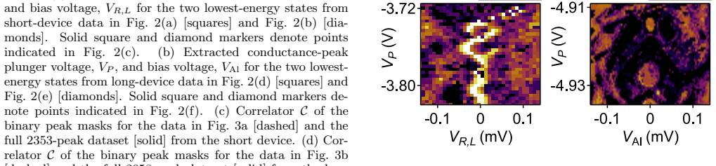
- [Fig. 2 caption] The caption of Fig. 2(c) refers to 'horizontal lines in Fig. 1(a,b)', which appears to be a cross-referencing error; the lines are shown in Fig. 2(a,b) of the same figure.
- [Main text, Fig. 3 discussion] The sentence 'In the short device, C is peaked around δV = 0. Including only the subset of data from Fig. 3(a) results in a correlator that is significantly less than unity' would be easier to interpret with the numerical peak values for the dashed traces in both panels.
- [Supplement Fig. S4] The comparison between the adaptive-binning and non-parametric mutual-information estimates is reassuring, but the red non-parametric value is shown as a single horizontal line without an uncertainty band; reporting a spread over bootstrap resamples would better quantify the binning dependence.
Circularity Check
No circularity: the correlator and mutual information are direct statistical measures of measured data, with error estimates from shifted datasets; no fitted parameter is renamed as a prediction.
full rationale
The paper's central quantities—the peak-mask correlator C in Eq. (1), the normalized mutual information NMI, and the pointwise NPMI—are computed directly from measured left/right conductances with no free parameters fitted to the data. The error bands in Fig. 3(c,d) are obtained by plunger-shifting one dataset, which is an independent statistical check rather than an assumed input. The length comparison (300 nm vs 900 nm) is an experimental comparison, not a derivation that reduces to its inputs. Self-citations appear only for platform development (SAG growth, refs. 30–31), a partner paper on finite-field effects (ref. 43), and standard mutual-information estimators (refs. 45–48); none of these is invoked as an unverified premise that forces the correlation result. The concern that the etched-Al ground may have finite impedance is a possible systematic effect on the physical interpretation, but it is not a circularity: the correlation metrics would still be what they are, and the claim that correlations reflect extended bound states is an interpretation of measured coincidences, not a quantity defined in terms of itself. No equation is constructed so that an output equals an input by definition, and no fitted parameter is later presented as a prediction. The derivation chain is self-contained as a statistical analysis of experimental data, so the circularity score is 0.
Assumptions & free parameters
free parameters (2)
- Peak-finding detection threshold =
not stated
- Adaptive binning cutoff (minimum samples per bin) =
80 points
assumptions (5)
- standard math Mutual information, normalized mutual information, and cross-covariance are valid measures of dependence for the measured conductance distributions.
- domain assumption The selective-area-grown aluminum terminal grounds the nanowire bulk without disrupting the Al-InAs interface, so the left and right conductance measurements are independent probes of each end.
- domain assumption Subgap peaks detected by the algorithm correspond to physical bound states, and coincident peaks at equal bias on both ends originate from the same state spanning the device.
- domain assumption The two biasing configurations (sweeping VR with VAl=0 vs sweeping VAl with VR=0) yield equivalent subgap spectroscopy.
- domain assumption Plunger-shifted datasets provide a valid null distribution for estimating the uncertainty of the correlator C.
Cite this review
Pith. "Pith review of End-to-end correlated subgap states in hybrid nanowires." pith.science (2026). https://pith.science/paper/77FGXKRQ
@misc{pith2026190805549,
  author       = {Pith},
  title        = {Pith review of: End-to-end correlated subgap states in hybrid nanowires},
  year         = {2026},
  howpublished = {\url{https://pith.science/paper/77FGXKRQ}},
  note         = {Machine review of arXiv:1908.05549}
}
abstract
End-to-end correlated bound states are investigated in superconductor-semiconductor hybrid nanowires at zero magnetic field. Peaks in subgap conductance are independently identified from each wire end, and a cross-correlation function is computed that counts end-to-end coincidences, averaging over thousands of subgap features. Strong correlations in a short, $300~\mathrm{nm}$ device are reduced by a factor of four in a long, $900~\mathrm{nm}$ device. In addition, subgap conductance distributions are investigated, and correlations between the left and right distributions are identified based on their mutual information.
Figures


Figures from the paper (1 more)
Reference graph
Works this paper leans on
-
[1]
A. Y. Kitaev, Physics-Uspekhi 44, 131 (2001)
2001
-
[2]
Kitaev, Annals of Physics 303, 2 (2003)
A. Kitaev, Annals of Physics 303, 2 (2003)
2003
-
[3]
Nayak, S
C. Nayak, S. H. Simon, A. Stern, M. Freedman, and S. Das Sarma, Rev. Mod. Phys. 80, 1083 (2008)
2008
-
[4]
R. M. Lutchyn, J. D. Sau, and S. Das Sarma, Phys. Rev. Lett. 105, 077001 (2010)
2010
-
[5]
Y. Oreg, G. Refael, and F. von Oppen, Phys. Rev. Lett. 105, 177002 (2010)
2010
-
[6]
Mourik, K
V. Mourik, K. Zuo, S. M. Frolov, S. R. Plissard, E. P. A. M. Bakkers, and L. P. Kouwenhoven, Science 336, 1003 (2012)
2012
-
[7]
A. Das, Y. Ronen, Y. Most, Y. Oreg, M. Heiblum, and H. Shtrikman, Nat. Phys 8, 887 (2012)
work page 2012
-
[8]
H. O. H. Churchill, V. Fatemi, K. Grove-Rasmussen, M. T. Deng, P. Caroff, H. Q. Xu, and C. M. Marcus, Phys. Rev. B 87, 241401(R) (2013)
work page 2013
Show all 48 references
-
[9]
M. T. Deng, S. Vaitiekenas, E. B. Hansen, J. Danon, M. Leijnse, K. Flensberg, J. Nyg˚ ard, P. Krogstrup, and C. M. Marcus, Science 354, 1557 (2016)
2016
-
[10]
Zhang, C.-X
H. Zhang, C.-X. Liu, S. Gazibegovic, D. Xu, J. A. Lo- gan, G. Wang, N. van Loo, J. D. S. Bommer, M. W. A. de Moor, D. Car, R. L. M. Op het Veld, P. J. van Veld- hoven, S. Koelling, M. A. Verheijen, M. Pendharkar, D. J. Pennachio, B. Shojaei, J. S. Lee, C. J. Palmstrøm, E. P. A...
2018
-
[11]
E. J. H. Lee, X. Jiang, M. Houzet, R. Aguado, C. M. Lieber, and S. De Franceschi, Nature Nanotechnology 9, 79 (2013)
2013
-
[12]
M.-T. Deng, S. Vaitiek˙ enas, E. Prada, P. San-Jose, J. Nyg˚ ard, P. Krogstrup, R. Aguado, and C. M. Marcus, Phys. Rev. B 98, 085125 (2018)
2018
-
[13]
Kells, D
G. Kells, D. Meidan, and P. W. Brouwer, Phys. Rev. B 86, 100503(R) (2012)
2012
-
[14]
Prada, P
E. Prada, P. San-Jose, and R. Aguado, Phys. Rev. B 86, 180503 (2012)
2012
-
[15]
Cayao, E
J. Cayao, E. Prada, P. San-Jose, and R. Aguado, Phys. Rev. B 91, 024514 (2015)
2015
-
[16]
San-Jose, J
P. San-Jose, J. Cayao, E. Prada, and R. Aguado, Scien- tific Reports 6, 21427 EP (2016)
2016
-
[17]
C.-X. Liu, J. D. Sau, T. D. Stanescu, and S. Das Sarma, Phys. Rev. B 96, 075161 (2017)
2017
-
[18]
A. Vuik, B. Nijholt, A. R. Akhmerov, and M. Wimmer, arXiv e-prints (2018), arXiv:1806.02801 [cond-mat.mes- hall]
2018 arXiv
-
[19]
C. Reeg, O. Dmytruk, D. Chevallier, D. Loss, and J. Kli- novaja, Physical Review B 98, 245407 (2018)
2018
-
[20]
S. M. Albrecht, A. Higginbotham, M. Madsen, F. Kuem- meth, T. S. Jespersen, J. Nyg˚ ard, P. Krogstrup, and C. M. Marcus, Nature 531, 206 (2016)
2016
-
[21]
Pe˜ naranda, R
F. Pe˜ naranda, R. Aguado, P. San-Jose, and E. Prada, Phys. Rev. B 98, 235406 (2018)
2018
-
[22]
A. M. Whiticar, A. Fornieri, E. C. T. O’Farrell, A. C. C. Drachmann, T. Wang, C. Thomas, S. Gronin, R. Kalla- her, G. C. Gardner, M. J. Manfra, C. M. Marcus, and F. Nichele, arXiv:1902.07085 (2019)
2019 arXiv
-
[23]
Das Sarma, J
S. Das Sarma, J. D. Sau, and T. D. Stanescu, Phys. Rev. B 86, 220506(R) (2012)
2012
-
[24]
B. M. Fregoso, A. M. Lobos, and S. Das Sarma, Phys. Rev. B 88, 180507(R) (2013)
2013
-
[25]
T. D. Stanescu and S. Tewari, Phys. Rev. B 89, 220507(R) (2014)
2014
-
[26]
T. O. Rosdahl, A. Vuik, M. Kjaergaard, and A. R. Akhmerov, Phys. Rev. B 97, 045421 (2018)
2018
-
[27]
Y.-H. Lai, J. D. Sau, and S. Das Sarma, arxiv:1901.02655 (2019)
2019 arXiv
-
[28]
Krogstrup, N
P. Krogstrup, N. L. B. Ziino, W. Chang, S. M. Albrecht, M. H. Madsen, E. Johnson, J. Nyg˚ ard, C. M. Marcus, and T. S. Jespersen, Nature Materials 14, 400 (2015), article
2015
-
[29]
Chang, S
W. Chang, S. M. Albrecht, T. S. Jespersen, F. Kuem- meth, P. Krogstrup, J. Nyg˚ ard, and C. M. Marcus, Na- ture Nanotechnology 10, 232 (2015)
2015
-
[30]
Krizek, J
F. Krizek, J. E. Sestoft, P. Aseev, S. Marti-Sanchez, S. Vaitiek˙ enas, L. Casparis, S. A. Khan, Y. Liu, T. Stankeviˇ c, A. M. Whiticar, A. Fursina, F. Boekhout, R. Koops, E. Uccelli, L. P. Kouwenhoven, C. M. Marcus, J. Arbiol, and P. Krogstrup, Physical Review Materials 2, 09...
2018
-
[31]
Vaitiek˙ enas, A
S. Vaitiek˙ enas, A. M. Whiticar, M.-T. Deng, F. Krizek, J. E. Sestoft, C. J. Palmstrøm, S. Marti-Sanchez, J. Ar- biol, P. Krogstrup, L. Casparis, and C. M. Marcus, Phys. Rev. Lett. 121, 147701 (2018)
2018
-
[32]
T. W. Larsen, K. D. Petersson, F. Kuemmeth, T. S. Jes- persen, P. Krogstrup, J. Nyg˚ ard, and C. M. Marcus, Phys. Rev. Lett. 115, 127001 (2015)
2015
-
[33]
Casparis, M
L. Casparis, M. R. Connolly, M. Kjaergaard, N. J. Pear- son, A. Kringhøj, T. W. Larsen, F. Kuemmeth, T. Wang, C. Thomas, S. Gronin, G. C. Gardner, M. J. Manfra, C. M. Marcus, and K. D. Petersson, Nature Nanotech- nology 13, 915 (2018)
2018
-
[34]
Plugge, A
S. Plugge, A. Rasmussen, R. Egger, and K. Flensberg, New Journal of Physics 19, 012001 (2017)
2017
-
[35]
Karzig, C
T. Karzig, C. Knapp, R. M. Lutchyn, P. Bonderson, M. B. Hastings, C. Nayak, J. Alicea, K. Flensberg, S. Plugge, Y. Oreg, C. M. Marcus, and M. H. Freed- man, Phys. Rev. B 95, 235305 (2017)
2017
-
[36]
Hofstetter, S
L. Hofstetter, S. Csonka, J. Nyg˚ ard, and C. Sch¨ onenberger, Nature461, 960 (2009)
2009
-
[37]
van Heck, S
B. van Heck, S. Mi, and A. R. Akhmerov, Phys. Rev. B 90, 155450 (2014)
2014
-
[38]
Strambini, S
E. Strambini, S. D’Ambrosio, F. Vischi, F. S. Bergeret, Y. V. Nazarov, and F. Giazotto, Nature Nanotechnology 11, 1055 (2016)
2016
-
[39]
J. S. Meyer and M. Houzet, Phys. Rev. Lett. 119, 136807 (2017)
2017
-
[40]
H.-Y. Xie, M. G. Vavilov, and A. Levchenko, Phys. Rev. B 96, 161406(R) (2017)
2017
-
[41]
Pankratova, H
N. Pankratova, H. Lee, R. Kuzmin, M. Vavilov, K. Wick- ramasinghe, W. Mayer, J. Yuan, J. Shabani, and V. E. M. Manucharyan, arXiv:1812.06017 (2018)
2018 arXiv
-
[42]
J. S. Lee, S. Choi, M. Pendharkar, D. J. Pennachio, B. Markman, M. Seas, S. Koelling, M. A. Verheijen, L. Casparis, K. D. Petersson, I. Petkovic, V. Schaller, M. J. Rodwell, C. M. Marcus, P. Krogstrup, L. P. Kouwenhoven, E. P. Bakkers, and C. J. Palmstrøm, arXiv:1808.04563 (2018)
2018 arXiv
-
[43]
G. C. M´ enard, G. L. R. Anselmetti, E. A. Martinez, D. Puglia, F. K. Malinowski, J. S. Lee, S. Choi, M. Pend- hakar, C. J. Palmstrøm, K. Flensberg, C. M. Marcus, L. Casparis, and A. P. Higginbotham, arXiv:1905.05505 (2019)
2019 arXiv
-
[44]
See Supplement, incl Ref.’s [45–48]
-
[45]
G. A. Darbellay and I. Vajda, IEEE Transactions on In- formation Theory 45, 1315 (1999)
1999
-
[46]
N. X. Vinh, J. Epps, and J. Bailey, Journal of Machine Learning Research 11, 2837 (2010)
2010
-
[47]
Kraskov, H
A. Kraskov, H. St¨ ogbauer, and P. Grassberger, Phys. Rev. E 69, 16 (2004), arXiv:0305641 [cond-mat]
2004
-
[48]
End-to-end correlated subgap states in hybrid nanowires
F. Pedregosa, G. Varoquaux, A. Gramfort, V. Michel, B. Thirion, O. Grisel, M. Blondel, P. Prettenhofer, R. Weiss, V. Dubourg, J. Vanderplas, A. Passos, D. Cour- napeau, M. Brucher, M. Perrot, and E. Duchesnay, Jour- nal of Machine Learning Research 12, 2825 (2011). 7 Supplemen...
2011
Reviewed August 14, 2026 · model on record in the stance chip above.
Discussion (0). Continue with ORCID to comment.