REVIEW 4 major objections 5 minor 28 references
Determination of fracture toughness of thin-film amorphous silicon using spiral crack structures
T0 review · 4 major / 5 minor · reviewed 2026-08-14 · deepseek-v4-flash
Pith's one-line read Spiral cracks peg amorphous silicon toughness at 4.7 MPa√m, about 5.7 times crystalline silicon.
desk verdict A plausible first K_Ic for solution-deposited a-Si from spiral cracks, but the central number rests on an assumed crack-growth rate the FEM prescribes rather than validates. read the letter →
The pith
A machine-rendered reading of the paper's core claim, the machinery that carries it, and where it could break.
The reading
What carries the argument
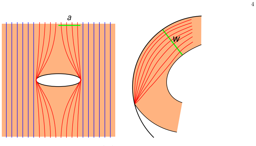
The carrying object is the spiral stripe width $w$, read as the analogue of Griffith's half crack length: every load path feeding the crack tip passes through this width, and the circular stress is nearly homogeneous across it. Around that analogy the argument builds a crack-growth simulation in which an initial diametric crack runs along the rim of a growing underetched disk, adding fresh stressed material ring by ring; the finite-element calculation supplies the geometry correction $f = 0.44$ and, through the equivalent stress intensity factor, selects the crack direction at each step. The machinery converts the measured quantities—Raman peak shift and stripe width—into the material property $K_{\mathrm{Ic}}$.
What would settle it
Etch identical stressed films at different underetch rates, for example by varying hydrofluoric acid concentration or temperature, and check whether the spiral stripe width changes while the Raman stress is unchanged; if $w$ shifts with etch rate, the rate-separation assumption fails. A second check is to compare the value $4.7$ MPa√m with a bulge-test or nanoindentation measurement on the same film.
Extended reading notes
Core claim
The central claim is that a spiral crack in an underetched film is mechanically equivalent to a Griffith crack whose characteristic half-length is the spiral stripe width $w$, so the crack-tip stress intensity factor is $K_I = \sigma \sqrt{\pi w}\,f$. The finite-element simulation supplies $f = 0.44$ and reproduces the observed spiral geometry, including the constant stripe width and the alternating overlap of lobes. Because the paper assumes crack growth is much faster than the etching front, the tip is always at the fracture threshold, so the identity becomes $K_{\mathrm{Ic}} = 0.44\,\sigma \sqrt{\pi w}$; with $\sigma$ from the Raman shift of the 480 cm$^{-1}$ a-Si:H peak, this yields $K_{\mathrm{Ic}}^{\mathrm{a-Si:H}} = 4.7(3)\,\mathrm{MPa}\sqrt{\mathrm{m}}$. The author regards this as the first determination of amorphous-silicon fracture toughness by this method and finds it plausible that the value exceeds crystalline silicon by a factor of 5.7.
Load-bearing premise
The load-bearing premise is that crack growth is so much faster than the underetching that the crack-tip stress intensity factor always sits at the fracture toughness; if the two rates are comparable, the stripe width would record etching kinetics rather than $K_{\mathrm{Ic}}$.
Editorial extensions
If this is right
- Amorphous silicon made from liquid polysilane precursor has $K_{\mathrm{Ic}} \approx 4.7$ MPa√m, about 5.7 times the value for crystalline silicon.
- Stripe width and residual stress determine each other once $K_{\mathrm{Ic}}$ is known, so measuring either quantity on a spiral-cracked film gives the other.
- The result applies to both single and double spirals, since after the first winding the local crack geometry and stress state coincide.
- The method suggests a simple destructive route to fracture toughness for any thin film that can be underetched into spiral cracks.
Reading between the lines
- If the rate-separation assumption transfers to other brittle films, the same stripe-width measurement could turn unwanted etching damage into routine toughness metrology for coatings, solar-cell layers, and MEMS films.
- A direct mechanical test of the analogy would be to vary the residual stress in one deposition series and verify $w \propto \sigma^{-2}$ at fixed $K_{\mathrm{Ic}}$; the paper proposes a version of this check but does not perform it.
- The large enhancement over crystalline silicon may imply that the disordered network suppresses cleavage-plane propagation, but the paper's data alone do not identify the microscopic mechanism.
- Because the Raman calibration is taken from crystalline silicon, a direct calibration of the 480 cm$^{-1}$ shift against a bendable substrate would tighten the absolute value; the author flags this as future work.
Signed reviews
Editorial analysis
A structured set of objections, weighed in public.
Referee Report
Summary. The manuscript reports spiral crack formation in hydrogenated amorphous silicon (a-Si:H) layers on glass after HF etching. The authors attribute the spirals to residual tensile stress, measured by Raman spectroscopy, and model the formation as a disk underetching whose boundary advances slowly while the crack tip advances at the fracture toughness. They propose a Griffith-type relation K_Ic = σ√(πw)f, identify the spiral stripe width w as the characteristic crack length, and use FEM simulations to obtain the geometry factor f = 0.44. Combining the Raman stress values with measured widths for four samples yields K_Ic = 4.7(3) MPa√m, about 5.7 times the crystalline-silicon value, claimed as the first determination of a-Si:H fracture toughness by this method.
Significance. If the central claim holds, this is a novel and potentially useful method for extracting thin-film fracture toughness from a simple destructive test. The strengths include a clear formation model, use of a standard FEM package, a transparent functional form for K_Ic, and an explicit list of limitations. The result is also significant because it extends the known trend that amorphous phases can be tougher than crystalline silicon. However, the quantitative claim rests on two unverified assumptions—quasi-static cracking at K_Ic and the transfer of the c-Si Raman calibration—and on a very small dataset, so the absolute value should be regarded as provisional pending direct validation. The paper does make a falsifiable prediction (σ ~ 1/√w) that could be tested with a wider sample set.
major comments (4)
- [MODEL OF CRACK FORMATION] The central assumption that crack growth is much faster than disk growth, so that the SIF at the crack tip always equals K_Ic, is stated but not experimentally validated. If the two rates are comparable, the observed stripe width w is set by the competition between etching and fracture kinetics, and the equation K_Ic = σ√(πw)f measures an effective process parameter rather than a material property. The FEM simulation cannot resolve this concern because step 2 of the simplified algorithm explicitly imposes SIF = K_Ic when choosing the rim-crack length; hence the constant stripe width and the value f = 0.44 are consequences of the assumption, not independent evidence for it. The authors should provide direct evidence of rate separation (e.g., time-resolved imaging of crack advance versus undercutting) or develop a coupled chemo-mechanical model to justify the quasi-static condition.
- [FEM SIMULATION] The paper states that the FEM 'confirms the analytical approach,' but the simplified algorithm uses a straight symmetric initial crack and grows it by finding the length for which SIF equals the fracture toughness. The qualitative match in Figure 6 and the fitted f = 0.44 therefore demonstrate self-consistency of the model, not an independent verification of the formation mechanism or of the SIF = K_Ic condition. To support f as a reliable geometry factor, the manuscript should provide convergence and mesh-dependence checks and a quantitative comparison of simulated and measured w for independently known σ and K_Ic values. The absence of such checks makes the 8% standard error reported in Eq. (7) incomplete, as it does not include any systematic uncertainty in f.
- [APPLICATION TO THE EXPERIMENTS AND DISCUSSION] Only four samples are used, with no reported uncertainty in w or Δω in Table I. From Table I, the products σ√w, which are proportional to K_Ic before the factor f, are approximately 6.2, 6.9, 6.1, and 4.6 GPa·μm^(1/2); sample #4 lies about 28% below the mean of the other three. This dataset is too small to test the predicted scaling σ ~ 1/√w or to establish the stated standard error of 8%. The authors should report per-sample measurement uncertainties and collect data over a wider range of stress values, as they themselves note is necessary in the Conclusions.
- [EXPERIMENTS] Equation (1) is calibrated for single-crystal silicon, and the paper applies it to a-Si:H based on reference [11]. Because the final K_Ic is directly proportional to σ, an unknown systematic offset in the a-Si:H piezo-Raman coefficient propagates linearly into the central claim. The manuscript acknowledges the need for a direct calibration in the Conclusions, but until such a calibration is performed, the absolute value 4.7(3) MPa√m should be regarded as provisional. I recommend performing the bendable-substrate calibration or at least quantifying the sensitivity of the result to this coefficient.
minor comments (5)
- [General] There are numerous typos that should be corrected in a revision: 'precurser' should be 'precursor', 'analythically' should be 'analytically', 'facture toughness' should be 'fracture toughness', 'Perfomed' should be 'Performed', 'relaxated' should be 'relaxed', and 'vanishs' should be 'vanishes'.
- [EXPERIMENTS] The text refers to 'the a-Si:H peak at 480 nm'; this should be 480 cm⁻¹. In addition, the unit in Eq. (1), written as 'MPa cm·Δω', is confusing because the 'cm' and 'cm⁻¹' cancel; it would be clearer to write the coefficient as 'MPa per cm⁻¹'.
- [Table I] The heading of Table I reads 'Measured shift if the a-Si:H Raman peak'; 'if' should be 'of'.
- [EXPERIMENTS] The statement that the two outer end points of the cracks are 'in opposite position to each other' is ambiguous; please specify whether they are 180° apart and whether this holds for both single and double spirals.
- [FEM SIMULATION] The FEM section does not list the material parameters (Young's modulus, Poisson's ratio, assumed K_Ic) used in the simulations; providing these together with mesh statistics would improve reproducibility. In addition, the equations in the manuscript are not consistently numbered or referenced, which makes the reading more difficult than necessary.
Circularity Check
No significant circularity: K_Ic comes from measured w, external Raman stress calibration, and an FEM geometry factor that is not fitted to the experimental fracture toughness.
full rationale
The derivation chain is not circular. Eq. (6) combines measured stripe widths w (Table I), Raman-based residual stress via the external single-crystal calibration eq. (1), and an FEM geometry factor f = 0.44. The FEM value is computed from elastic stress-intensity calculations for the spiral geometry; although the simulation uses the formation-model condition SIF = K_Ic in its crack-growth rule, this implements the paper's explicitly stated quasistatic assumption rather than importing the experimental K_Ic back into the fit. The simulated points in Fig. 7 are generated with assumed K_Ic and σ values, so f is a genuinely computed geometry correction, not a renamed experimental parameter. The only self-citation ([1]) supports background on the liquid-precursor material and is not load-bearing for the toughness determination; the Raman calibration and Griffith/SIF relationships come from external sources. The paper itself flags the unverified σ ∼ 1/√w scaling and the need to calibrate eq. (1) for a-Si:H; these are explicit limitations affecting confidence in the model, not circular reductions. The rate-separation assumption, if false, would undermine the measurement concept, but that is a correctness/falsifiability risk rather than a step in which the conclusion is assumed by construction.
Assumptions & free parameters
free parameters (1)
- FEM geometry factor f_spiral =
0.44
assumptions (6)
- domain assumption Eq. (1) calibration for single-crystal silicon (σ = -249 MPa·cm · Δω) applies quantitatively to the amorphous silicon peak at 480 cm⁻¹.
- domain assumption The Griffith formula applies to the spiral with the stripe width w as the characteristic crack length (eq. 2 with a = w).
- domain assumption Crack growth is much faster than undercutting, so the stress intensity factor at the crack tip always equals K_Ic.
- domain assumption The underetched region is a growing disk with uniform biaxial stress, and the crack follows its rim.
- ad hoc to paper The simplified FEM crack-growth algorithm (straight initial crack through the diameter, symmetric mirror tip, ring addition) faithfully reproduces the real spiral evolution.
- standard math SIF = σ√(πa)f and the equivalent-SIF crack-direction criteria [13,14] are valid.
Cite this review
Pith. "Pith review of Determination of fracture toughness of thin-film amorphous silicon using spiral crack structures." pith.science (2026). https://pith.science/paper/UHFP2324
@misc{pith2026190806518,
  author       = {Pith},
  title        = {Pith review of: Determination of fracture toughness of thin-film amorphous silicon using spiral crack structures},
  year         = {2026},
  howpublished = {\url{https://pith.science/paper/UHFP2324}},
  note         = {Machine review of arXiv:1908.06518}
}
read the original abstract
We prepared thin layers of amorphous silicon by deposition of a liquid-phase polysilane precurser on glass substrate. Raman scattering provides evidence for residual tensile stress in the silicon, which is evaluated quantitatively. Under treatment with hydrofluoric acid, this stress leads to spiral cracks in the silicon. We explain the process of crack formation and examine this phenomenon both analytically and numerically, the latter with the finite element method (FEM). The FEM yields the geometry correction factor for such spiral cracks in terms of the Griffith criterion. This allows for the first time the determination of fracture toughness of amorphous silicon, which is greatly enhanced in comparison with crystalline silicon.
Figures


Figures from the paper (3 more)


Reference graph
Works this paper leans on
-
[19]
It has been frequently reported (e
reports a lower limit ofKIc of a-Si:H at 1.35 MPa√m. It has been frequently reported (e. g. by [19, 20]) that 6 amorphous phases exceed their crystalline counterparts in fracture toughness, sometimes by more than a decade. Thus, we consider the above K a-Si:H Ic in plausible accor- dance with previous findings. We consider the variation of the measured str...
-
[11]
E. Anastassakis, A. Pinczuk, E. Burstein, F. Pollak, and M. Cardona, Effect of static uniaxial stress on the raman spectrum of silicon, solid state Communications 8, 133 (1970)
work page 1970
-
[1]
Any initial crack, originating at the centre of the disk, grows straight towards the rim
-
[2]
Any small deviation from the straight line makes the other tip of the crack deviate in the same di- rection (e. g. clockwise). In other words, the tips 5 try to evade each other
-
[3]
When the crack propagates along the rim, its growth direction points outwards. Thus, it must stay on the rim. Another trivial observation is that a symmetric initial crack (e. g. straight through the centre over the total di- ameter) conserves symmetry over the whole simulation. This means that only one crack tip has to be analysed, and the other one just...
-
[4]
Create a straight initial crack through the total di- ameter of the initial disk
-
[5]
Find the length of the crack on the rim of the disk for which the SIF at the tip equals the fracture toughness of the material, and let the crack grow to this length
-
[6]
This brings new stress into the material, and the crack can grow further
Add another ring of finite elements around the disk. This brings new stress into the material, and the crack can grow further
Show all 28 references
-
[7]
Otherwise, end the simu- lation
If the winding number of the spiral is below a pre- set value, go back to (2). Otherwise, end the simu- lation. Figure 6 presents the result of the FEM in an illustra- tive manner: The finite elements are displaced according to the values of tension in the spiral lobes. This wa...
-
[8]
S. Chan, I. Tuba, and W. Wilson, On the finite element method in linear fracture mechanics, Engineering Frac- ture Mechanics 2, 1 (1970)
1970
-
[9]
Bronger, P
T. Bronger, P. H. W¨ obkenberg, J. W¨ ordenweber, S. Muthmann, U. W. Paetzold, V. Smirnov, S. Traut, ¨U. Dagkaldiran, S. Wieber, M. C¨ olle, et al. , Solution- based silicon in thin-film solar cells, Advanced Energy Materials (2014)
2014
-
[10]
Stutzmann, Role of mechanical stress in the light- induced degradation of hydrogenated amorphous silicon, Applied Physics Letters 47, 21 (1985)
M. Stutzmann, Role of mechanical stress in the light- induced degradation of hydrogenated amorphous silicon, Applied Physics Letters 47, 21 (1985)
1985
-
[12]
De Wolf, Micro-raman spectroscopy to study local me- chanical stress in silicon integrated circuits, Semiconduc- tor Science and Technology 11, 139 (1996)
I. De Wolf, Micro-raman spectroscopy to study local me- chanical stress in silicon integrated circuits, Semiconduc- tor Science and Technology 11, 139 (1996)
1996
-
[13]
Anastassakis, A
E. Anastassakis, A. Cantarero, and M. Cardona, Piezo- raman measurements and anharmonic parameters in sil- icon and diamond, Physical Review B 41, 7529 (1990)
1990
-
[14]
Griffith, Vi
A. Griffith, Vi. the phenomena of rupture and flow in solids., Phil. Trans. Roy. Soc. (Lon.) A 221, 163 (1920)
1920
-
[15]
G. R. Irwin, Analysis of stresses and strains near the end of a crack traversing a plate, J. appl. Mech. (1957)
1957
-
[16]
Chasiotis, S
I. Chasiotis, S. Cho, and K. Jonnalagadda, Fracture toughness and subcritical crack growth in polycrystalline silicon, Journal of applied mechanics 73, 714 (2006)
2006
-
[17]
G. E. Blandford, A. R. Ingraffea, and J. A. Liggett, Two- dimensional stress intensity factor computations using the boundary element method, International Journal for Numerical Methods in Engineering 17, 387 (1981)
1981
-
[18]
Anastassakis, Physical problems in microelectron- ics, Proceedings of the 4th International School ISPPM, Varna, Bulgaria , 128 (1985)
E. Anastassakis, Physical problems in microelectron- ics, Proceedings of the 4th International School ISPPM, Varna, Bulgaria , 128 (1985)
1985
-
[20]
J. Ge, R. Stangl, A. AG, and T. Mueller, Detailed micro raman spectroscopy analysis of doped silicon thin film layers and its feasibility for heterojunction silicon wafer solar cells, Journal of Materials Science and Chemical Engineering 2013 (2013)
2013
-
[21]
Cimrman et al
R. Cimrman et al. , Sfepy: Simple finite elements in python (2008)
2008
-
[22]
Richard, M
H. Richard, M. Fulland, and M. Sander, Theoretical crack path prediction, Fatigue & Fracture of Engineering Ma- terials & Structures 28, 3 (2005)
2005
-
[23]
A. M. Alshoaibi and A. K. Ariffin, Finite element sim- ulation of stress intensity factors in elastic-plastic crack growth, Journal of Zhejiang University Science A 7, 1336 (2006)
2006
-
[24]
L. L. Mercado, H. Wieser, and T. Hauck, Multichip pack- age delamination and die fracture analysis, Advanced Packaging, IEEE Transactions on 26, 152 (2003)
2003
-
[25]
Bagdahn, J
J. Bagdahn, J. Schischka, M. Petzold, and W. N. Sharpe Jr, Fracture toughness and fatigue investigations of polycrystalline silicon, in Micromachining and Micro- fabrication (International Society for Optics and Photon- ics, 2001) pp. 159–168
2001
-
[26]
H. Kahn, N. Tayebi, R. Ballarini, R. Mullen, and A. Heuer, Fracture toughness of polysilicon mems de- vices, Sensors and Actuators A: Physical 82, 274 (2000)
2000
-
[27]
J. G. Swadener and M. Nastasi, Increasing the fracture toughness of silicon by ion implantation, Nuclear Instru- ments and Methods in Physics Research Section B: Beam Interactions with Materials and Atoms 206, 937 (2003)
2003
-
[28]
Gilbert, J, R
C. Gilbert, J, R. Ritchie, and W. Johnson, Fracture toughness and fatigue-crack propagation in a zr–ti–ni– cu–be bulk metallic glass, Applied Physics Letters 71, 476 (1997)
1997
Reviewed August 14, 2026 · model on record in the stance chip above.
Discussion (0). Continue with ORCID to comment.