REVIEW 4 major objections 6 minor 57 references
Influence of irradiation on defect spin coherence in silicon carbide
T0 review · 4 major / 6 minor · reviewed 2026-08-14 · deepseek-v4-flash
Pith's one-line read The paper establishes that irradiation-induced spin decoherence in 4H-SiC follows one universal scaling with emitter density, $T_2 = T_2^{\mathrm{pristine}}/(1+T_2^{\mathrm{pristine}}\kappa N_V)$, across electron, neutron, and proton…
desk verdict A genuinely useful systematic dataset for SiC emitter coherence, dressed up with a 'universal scaling' that is really a per-irradiation fit formula. read the letter →
The pith
A machine-rendered reading of the paper's core claim, the machinery that carries it, and where it could break.
The reading
What carries the argument
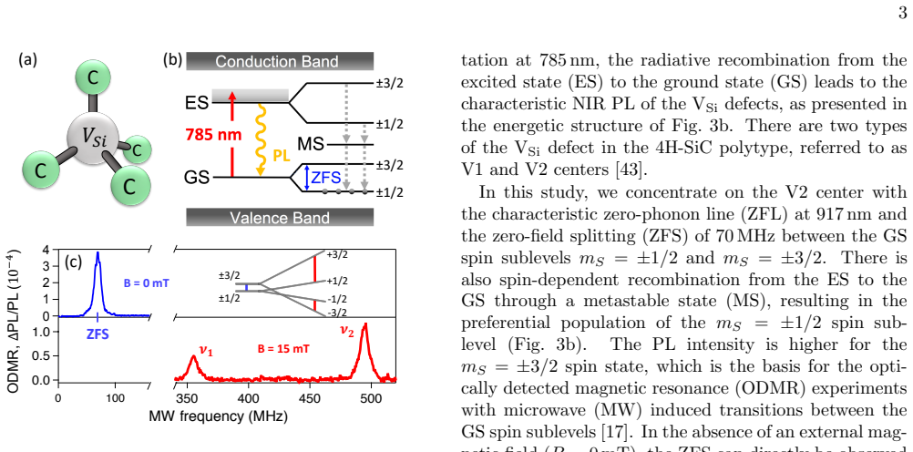
The load-bearing object is the negatively charged silicon vacancy in 4H-SiC (the V2 center, an $S=3/2$ defect spin read out by pulsed optically detected magnetic resonance, ODMR), and the load-bearing identity is the two-parameter formula $T_2 = T_2^{\mathrm{pristine}}/(1+T_2^{\mathrm{pristine}}\kappa N_V)$. The mechanism behind it is additive spin-bath decoherence: separate channels from nuclear spins, paramagnetic impurities, residual defects, and irradiation-induced defects each contribute a rate, and the irradiation channel is taken to be proportional to the optically active emitter density $N_V$. The formula does the work of collapsing data taken with neutrons, electrons, and protons of several energies onto one family of curves, with $\kappa$ parameterizing how much collateral damage each irradiation type produces per useful vacancy.
What would settle it
A decisive test is to measure $T_2$ in electron-irradiated samples with the same emitter density $N_V\approx 10^{15}\,\mathrm{cm}^{-3}$ produced at 1 MeV and at 25 MeV: the formula with a single $\kappa$ predicts identical $T_2$, so any resolvable difference would falsify the energy-independence claim. A second target: for one irradiation type, vary fluence across several $N_V$ values and check that $T_2^{\mathrm{pristine}}/T_2-1$ is exactly linear in $N_V$ with zero intercept; curvature would show that the irradiation decoherence rate is not simply proportional to $N_V$.
Extended reading notes
Core claim
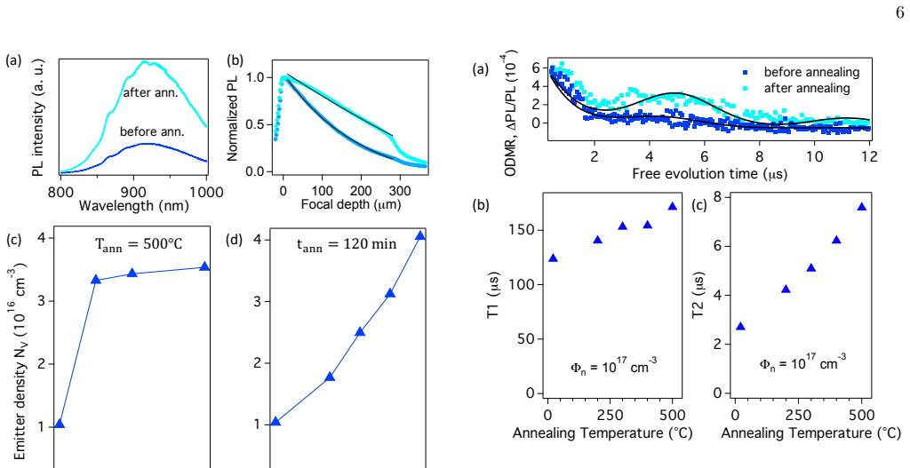
On the paper's own terms, the discovery is a common scaling curve for irradiation-induced decoherence of the V2 silicon-vacancy spin in 4H-SiC. The decoherence rate is written as $1/T_2 = 1/T_2^{(n)}+1/T_2^{(p)}+1/T_2^{(r)}+1/T_2^{(i)}$, with the nuclear contribution $1/T_2^{(n)}$ suppressed by a 15 mT field, and the irradiation contribution assumed to grow linearly with the density of optically active vacancies: $1/T_2^{(i)}=\kappa N_V$. The resulting expression $T_2 = T_2^{\mathrm{pristine}}/(1+T_2^{\mathrm{pristine}}\kappa N_V)$ describes all measured electron, neutron, and proton data with two independent parameters; electron irradiation gives $\kappa=0.8\times 10^{-11}\,\mathrm{s^{-1}}\,\mathrm{cm^3}$, neutron irradiation gives larger $\kappa$ values ($3.8$ and $25.2\times 10^{-11}\,\mathrm{s^{-1}}\,\mathrm{cm^3}$ in the two reactors used), and proton data approach the same law. $T_1$ stays essentially constant at about 300 $\mu$s up to $N_V=7\times 10^{15}\,\mathrm{cm}^{-3}$, showing that spin-lattice relaxation is an intrinsic spin-phonon (Raman) property rather than an irradiation effect. Annealing a heavily neutron-irradiated sample raises $T_2$ by a factor of about 2.5 without removing the VSi centers, which the authors attribute to healing of other paramagnetic defects.
Load-bearing premise
The assumption the whole scaling rests on is that each additional optically active silicon vacancy adds exactly the same decoherence rate $1/T_2^{(i)}=\kappa N_V$, regardless of irradiation type, particle energy, or local damage structure; if that proportionality breaks, Eq. (1) is only a curve fit and the claimed universality collapses.
Editorial extensions
If this is right
- Once $\kappa$ for a given beam line or reactor is known, Eq. (1) predicts $T_2$ at any fluence, so irradiation recipes can be designed to hit a target coherence time without trial-and-error.
- Electron irradiation is the gentlest route to dense coherent ensembles, while neutron irradiation buys higher volume density at the price of shorter $T_2$; annealing recovers part of that loss.
- $T_1$'s insensitivity up to $7\times 10^{15}\,\mathrm{cm}^{-3}$ means the spin-lattice limit will not bottleneck quantum operations in that density range, leaving $T_2$ as the controlling figure of merit.
- The same two-parameter curve should organize published and future data for other irradiation particles and energies once $N_V$ and $T_2^{\mathrm{pristine}}$ are fixed, making the result a benchmark for device-oriented studies.
Reading between the lines
- If the proportionality is exact, $\kappa$ becomes a direct measure of collateral damage per useful emitter, so comparing $\kappa$ across irradiation types should correlate with computed displacement damage and could be predicted from stopping-power simulations.
- The same collapse plot could be applied to divacancy and other spin defects in SiC: if their decoherence is also dominated by irradiation-induced paramagnetic defects, their $T_2$ should fall on the same functional form with a defect-specific $\kappa$.
- The annealing results suggest a separate route to high coherence: irradiate densely and then selectively heal non-vacancy defects below the vacancy-annealing temperature; testing intermediate temperatures between $500$ and $700\,^{\circ}\mathrm{C}$ would map the trade-off between recovered $T_2$ and lost $N_V$.
Signed reviews
Editorial analysis
A structured set of objections, weighed in public.
Referee Report
Summary. The manuscript reports a systematic pulsed ODMR study of T1 and T2 for silicon vacancies in 4H-SiC after neutron, electron, and proton irradiation over wide fluence ranges, including annealing experiments. The central claim is that T2 follows a universal scaling with the optically active emitter density NV, T2 = T2_pristine / (1 + T2_pristine kappa NV), with T2_pristine and kappa as the only parameters, and that T1 remains near 300 microseconds up to NV ≈ 7x10^15 cm^-3. The data include new measurements and literature points, and the paper proposes this scaling as a design rule for choosing irradiation conditions.
Significance. If the proposed scaling were established, it would provide a practically useful rule for estimating T2 from NV and irradiation type. The paper's dataset is valuable: it compares multiple irradiation particles and energies, demonstrates T1 robustness, and shows annealing can partially recover T2. However, the central universal-scaling claim currently rests on fitting Eq. (1) with irradiation-type-dependent kappa values and an untested proportionality between decoherence rate and the PL-derived NV, so the paper's significance is diminished until the scaling is substantiated with independent calibrations and uncertainty-aware fits.
major comments (4)
- [Discussion, Eq. (1); Conclusion] The claimed universal scaling is not supported because kappa is not a single parameter across the data. The fits use kappa = 0.8x10^-11, 3.8x10^-11, and 25.2x10^-11 s^-1 cm^3 for electron, BER II neutron, and TRIGA neutron irradiations, respectively. With a different kappa per irradiation condition, Eq. (1) becomes a parametrization, and the concluding statement that 'all data can be well described by the same equation with two independent parameters' is misleading because the two parameters are re-fit per data set. To claim universality, the authors would need to show kappa is determined by known irradiation parameters (e.g., particle type, energy, or displacement cross-section) and to test the scaling form with at least one parameter-free prediction.
- [Discussion: 'We assume that 1/T2^(i) is proportional to the number of all irradiation induced defects...'] This assumption is the load-bearing premise of Eq. (1), but it is not tested. NV is calibrated from PL intensity of optically active VSi centers (Results, Fig. 2), not from the total irradiation-induced defect concentration. The authors themselves note that PL drops at high fluence because non-radiative defects dominate while total damage increases; indeed, they report a deviation from Eq. (1) for NV > 7x10^15 cm^-3. In the absence of an independent measure of total defect density, the linear relation 1/T2^(i) = kappa NV is an unverified proxy, and the model's claimed predictive power is not established. The manuscript should either provide independent evidence for this proportionality (e.g., from EPR or absorption measurements) or explicitly limit the claim to the regime where PL-derived NV is monotonic in fluence.
- [Discussion, neutron-irradiated samples] The authors state that coherence times of neutron-irradiated samples 'should be seen as a lower bound' because of microwave-field inhomogeneity. If T2 is a lower bound, then the fitted kappa values for neutron data (3.8x10^-11 and 25.2x10^-11 s^-1 cm^3) are not reliable: the true T2 may be longer and kappa correspondingly smaller. Fitting lower-bound data to extract kappa and then comparing these kappa values with electron data biases the conclusion that neutron irradiation produces a larger decoherence per emitter. These points should either be corrected with homogeneous-pulse measurements or excluded from quantitative kappa extraction, with the qualitative trend stated separately.
- [Results, Fig. 5; Methods] The manuscript does not report uncertainties for the fitted parameters T2_pristine and kappa, and many T2 data points in Fig. 5b lack error bars. Without these, the statement that the data are 'well described' by Eq. (1) cannot be assessed, and the comparison of kappa values across irradiation types is not meaningful. Please report standard errors or confidence intervals for all fitted parameters, and show fit residuals or include the number of data points and goodness-of-fit metrics. The same applies to the T1 = 300 microseconds plateau, for which only representative error bars are shown.
minor comments (6)
- [Introduction and Results] The abbreviation 'ZFL' in 'zero-phonon line (ZFL)' should be 'ZPL'.
- [Fig. 4c caption] 'varyable delay time' should be 'variable delay time'.
- [Discussion] 'inrease' should be 'increase'.
- [Fig. 5 caption] 'red close symbols' should be 'red closed symbols'.
- [Fig. 2 axes] The axis labels appear garbled as 'N#(cm&')' and similar; please ensure correct typesetting of the emitter-density and fluence units.
- [Results, NV calibration] The NV calibration is described only by reference [25]; please add a short description of the calibration procedure and its uncertainty in the Methods section.
Circularity Check
No significant circularity: Eq. (1) is an explicitly stated linear modeling assumption fitted to data, not a hidden reduction or an out-of-sample prediction.
full rationale
The paper's central scaling law, Eq. (1), is not derived by circular reasoning. In the Discussion the authors explicitly declare the load-bearing input: 'We assume that 1/T2^(i) is proportional to the number of all irradiation induced defects, which in turn scales with NV.' Equation (1) is merely the algebraic rearrangement of that assumption together with additive decoherence rates. The parameters T2^(pristine) and κ are then fitted to the measured T2(NV) data, and the paper uses the language 'fitted' and 'described' rather than presenting an independent, parameter-free prediction. Varying κ across electron and neutron irradiations is disclosed ('They can be described assuming κ = 3.8 × 10^-11 s^-1 cm^3 and κ = 25.2 × 10^-11 s^-1 cm^3'), and the authors further concede that for ion irradiation 'κ should depend on the ion type and energy as well as on the depth from the irradiated surface.' The neutron T2 values are explicitly identified as lower bounds due to microwave-field inhomogeneity. The NV calibration cites the authors' prior work [25], but this is an experimental calibration of PL intensity, not a theorem used to forbid alternatives; it does not by construction generate the T2(NV) relationship. Thus, while the universality claim is only as strong as the untested proportionality assumption, that assumption is openly stated and is not a circular reduction of the paper's input into its output.
Assumptions & free parameters
free parameters (5)
- T2_pristine =
48 microseconds for main electron and neutron fits; 100 microseconds for the literature-sample dashed fit
- kappa (electron irradiation) =
0.8 x 10^-11 s^-1 cm^3
- kappa (neutron irradiation, BER II reactor) =
3.8 x 10^-11 s^-1 cm^3
- kappa (neutron irradiation, TRIGA reactor) =
25.2 x 10^-11 s^-1 cm^3
- Literature N_V estimate for Carter sample =
approximately 10^15 cm^-3
assumptions (5)
- ad hoc to paper 1/T2^(i) is proportional to the number of all irradiation-induced defects, which in turn scales with N_V.
- domain assumption T1 is dominated by the Raman spin-phonon mechanism, which is intrinsic to SiC and independent of irradiation fluence.
- domain assumption The photoluminescence intensity is proportional to N_V through a calibration using a reference 4H-SiC sample of known N_V.
- domain assumption Electron irradiation produces a nearly homogeneous VSi distribution across the 300 micrometer sample thickness at 1 to 25 MeV.
- domain assumption Thermal neutrons produce negligible displacement, so only epithermal and fast neutron fluences are counted.
Cite this review
Pith. "Pith review of Influence of irradiation on defect spin coherence in silicon carbide." pith.science (2026). https://pith.science/paper/O42UOL2L
@misc{pith2026190806829,
  author       = {Pith},
  title        = {Pith review of: Influence of irradiation on defect spin coherence in silicon carbide},
  year         = {2026},
  howpublished = {\url{https://pith.science/paper/O42UOL2L}},
  note         = {Machine review of arXiv:1908.06829}
}
abstract
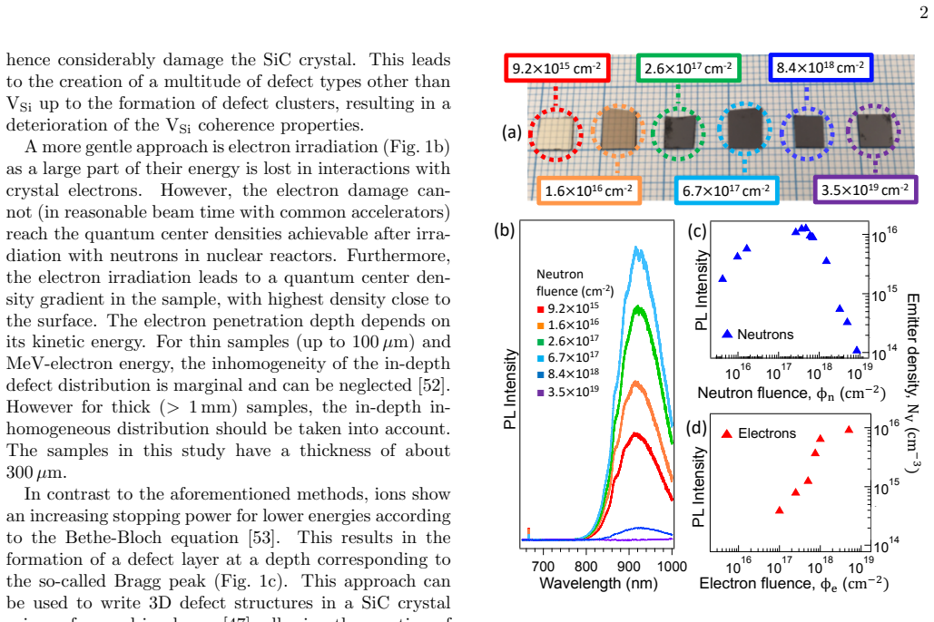
Irradiation-induced lattice defects in silicon carbide (SiC) have already exceeded their previous reputation as purely performance-inhibiting. With their remarkable quantum properties, such as long room-temperature spin coherence and the possibility of downscaling to single-photon source level, they have proven to be promising candidates for a multitude of quantum information applications. One of the most crucial parameters of any quantum system is how long its quantum coherence can be preserved. By using the pulsed optically detected magnetic resonance (ODMR) technique, we investigate the spin-lattice relaxation time ($T_1$) and spin coherence time ($T_2$) of silicon vacancies in 4H-SiC created by neutron, electron and proton irradiation in a broad range of fluences. We also examine the effect of irradiation energy and sample annealing. We establish a robustness of the $T_1$ time against all types of irradiation and reveal a universal scaling of the $T_2$ time with the emitter density. Our results can be used to optimize the coherence properties of silicon vacancy qubits in SiC for specific tasks.
Figures

Figures from the paper (3 more)


Reference graph
Works this paper leans on
-
[1]
P. G. Baranov, A. P. Bundakova, A. A. Soltamova, S. B. Orlinskii, I. V. Borovykh, R. Zondervan, R. Verberk, and J. Schmidt, Silicon vacancy in SiC as a promising quantum system for single-defect and single-photon spec- troscopy, Physical Review B 83, 125203 (2011)
work page 2011
-
[2]
W. F. Koehl, B. B. Buckley, F. J. Heremans, G. Calu- sine, and D. D. Awschalom, Room temperature coherent control of defect spin qubits in silicon carbide, Nature 479, 84 (2011)
2011
- [3]
-
[4]
J. R. Weber, W. F. Koehl, J. B. Varley, A. Janotti, B. B. Buckley, C. G. Van de Walle, and D. D. Awschalom, Quantum computing with defects, Proceedings of the Na- tional Academy of Sciences 107, 8513 (2010)
2010
-
[5]
A. L. Falk, B. B. Buckley, G. Calusine, W. F. Koehl, V. V. Dobrovitski, A. Politi, C. A. Zorman, P. X. L. Feng, and D. D. Awschalom, Polytype control of spin qubits in silicon carbide, Nature Communications 4, 1819 (2013)
work page 2013
-
[6]
L.-P. Yang, C. Burk, M. Widmann, S.-Y. Lee, J. Wrachtrup, and N. Zhao, Electron spin decoherence in silicon carbide nuclear spin bath, Physical Review B 90, 241203 (2014)
work page 2014
-
[7]
S. G. Carter, ¨O. O. Soykal, P. Dev, S. E. Economou, and E. R. Glaser, Spin coherence and echo modulation of the silicon vacancy in 4H-SiC at room temperature, Physical Review B 92, 161202 (2015)
2015
-
[8]
H. Seo, A. L. Falk, P. V. Klimov, K. C. Miao, G. Galli, and D. D. Awschalom, Quantum decoherence dynamics of divacancy spins in silicon carbide, Nature Communi- cations 7, 12935 (2016)
work page 2016
Show all 57 references
-
[9]
Simin, H
D. Simin, H. Kraus, A. Sperlich, T. Ohshima, G. V. As- takhov, and V. Dyakonov, Locking of electron spin co- herence above 20 ms in natural silicon carbide, Physical Review B 95, 161201(R) (2017)
2017
-
[10]
Fischer, A
M. Fischer, A. Sperlich, H. Kraus, T. Ohshima, G. V. Astakhov, and V. Dyakonov, Highly Efficient Optical Pumping of Spin Defects in Silicon Carbide for Stimu- lated Microwave Emission, Physical Review Applied 9, 2126 (2018)
2018
-
[11]
P. G. Brereton, D. Puent, J. Vanhoy, E. R. Glaser, and S. G. Carter, Spin coherence as a function of implantation depth for silicon vacancies in proton-irradiated 4H-SiC, arXiv:1812.10432
-
[12]
V. A. Soltamov, C. Kasper, A. V. Poshakinskiy, A. N. Anisimov, E. N. Mokhov, A. Sperlich, S. A. Tarasenko, P. G. Baranov, G. V. Astakhov, and V. Dyakonov, Exci- tation and coherent control of spin qudit modes in silicon carbide at room temperature, Nature Communications 10, 16...
2019
-
[13]
Kraus, V
H. Kraus, V. A. Soltamov, D. Riedel, S. V¨ ath, F. Fuchs, A. Sperlich, P. G. Baranov, V. Dyakonov, and G. V. As- takhov, Room-temperature quantum microwave emitters based on spin defects in silicon carbide, Nature Physics 10, 157 (2014)
2014
-
[14]
A. L. Falk, P. V. Klimov, B. B. Buckley, V. Iv´ ady, I. A. Abrikosov, G. Calusine, W. F. Koehl, A. Gali, and D. D. Awschalom, Electrically and Mechanically Tunable Elec- tron Spins in Silicon Carbide Color Centers, Physical Re- view Letters 112, 187601 (2014)
2014
-
[15]
¨O. O. Soykal and T. L. Reinecke, Quantum metrology with a single spin-3/2 defect in silicon carbide, Physical Review B 95, 081405 (2017)
2017
-
[16]
Castelletto, B
S. Castelletto, B. C. Johnson, and A. Boretti, Quantum Effects in Silicon Carbide Hold Promise for Novel Inte- grated Devices and Sensors, Advanced Optical Materials 1, 609 (2013)
2013
-
[17]
Kraus, V
H. Kraus, V. A. Soltamov, F. Fuchs, D. Simin, A. Sper- lich, P. G. Baranov, G. V. Astakhov, and V. Dyakonov, Magnetic field and temperature sensing with atomic-scale spin defects in silicon carbide, Scientific Reports 4, 5303 (2014)
2014
-
[18]
Simin, F
D. Simin, F. Fuchs, H. Kraus, A. Sperlich, P. G. Baranov, G. V. Astakhov, and V. Dyakonov, High-Precision Angle- Resolved Magnetometry with Uniaxial Quantum Centers in Silicon Carbide, Physical Review Applied 4, 014009 (2015)
2015
-
[19]
S.-Y. Lee, M. Niethammer, and J. Wrachtrup, Vector magnetometry based on S=3/2 electronic spins, Physical Review B 92, 115201 (2015)
2015
-
[20]
Simin, V
D. Simin, V. A. Soltamov, A. V. Poshakinskiy, A. N. Anisimov, R. A. Babunts, D. O. Tolmachev, E. N. Mokhov, M. Trupke, S. A. Tarasenko, A. Sperlich, P. G. Baranov, V. Dyakonov, and G. V. Astakhov, All-Optical dc Nanotesla Magnetometry Using Silicon Vacancy Fine Structure in Is...
2016
-
[21]
Niethammer, M
M. Niethammer, M. Widmann, S.-Y. Lee, P. Stenberg, O. Kordina, T. Ohshima, N. T. Son, E. Janz´ en, and J. Wrachtrup, Vector Magnetometry Using Silicon Va- cancies in 4H-SiC Under Ambient Conditions, Physical Review Applied 6, 034001 (2016)
2016
-
[22]
C. J. Cochrane, J. Blacksberg, M. A. Anders, and P. M. Lenahan, Vectorized magnetometer for space applica- tions using electrical readout of atomic scale defects in silicon carbide, Scientific Reports 6, 37077 (2016)
2016
-
[23]
A. N. Anisimov, D. Simin, V. A. Soltamov, S. P. Lebe- dev, P. G. Baranov, G. V. Astakhov, and V. Dyakonov, Optical thermometry based on level anticrossing in sili- con carbide, Scientific Reports 6, 33301 (2016)
2016
-
[24]
Castelletto, B
S. Castelletto, B. C. Johnson, V. Iv´ ady, N. Stavrias, T. Umeda, A. Gali, and T. Ohshima, A silicon carbide room-temperature single-photon source, Nature Materi- 9 als 13, 151 (2013)
2013
-
[25]
Fuchs, B
F. Fuchs, B. Stender, M. Trupke, D. Simin, J. Pflaum, V. Dyakonov, and G. V. Astakhov, Engineering near- infrared single-photon emitters with optically active spins in ultrapure silicon carbide, Nature Communications 6, 7578 (2015)
2015
-
[26]
D. J. Christle, A. L. Falk, P. Andrich, P. V. Klimov, J. u. Hassan, N. T. Son, E. Janz´ en, T. Ohshima, and D. D. Awschalom, Isolated electron spins in silicon carbide with millisecond coherence times, Nature Materials 14, 160 (2015)
2015
-
[27]
Widmann, S.-Y
M. Widmann, S.-Y. Lee, T. Rendler, N. T. Son, H. Fedder, S. Paik, L.-P. Yang, N. Zhao, S. Yang, I. Booker, A. Denisenko, M. Jamali, S. A. Momen- zadeh, I. Gerhardt, T. Ohshima, A. Gali, E. Janz´ en, and J. Wrachtrup, Coherent control of single spins in silicon carbide at room ...
2015
-
[28]
D. J. Christle, P. V. Klimov, C. F. de las Casas, K. n. Sz sz, V. Iv dy, V. Jokubavicius, J. Ul Hassan, M. Syv j rvi, W. F. Koehl, T. Ohshima, N. T. Son, E. Janz n, d. m. Gali, and D. D. Awschalom, Isolated Spin Qubits in SiC with a High-Fidelity Infrared Spin-to-Photon Interf...
2017
-
[29]
R. Nagy, M. Niethammer, M. Widmann, Y.-C. Chen, P. Udvarhelyi, C. Bonato, J. u. Hassan, R. Karhu, I. G. Ivanov, N. T. Son, J. R. Maze, T. Ohshima,¨O. O. Soykal, A. Gali, S.-Y. Lee, F. Kaiser, and J. Wrachtrup, High- fidelity spin and optical control of single silicon-vacancy ce...
2019
-
[30]
H. B. Banks, ¨O. O. Soykal, R. Myers-Ward, D. K. Gaskill, T. L. Reinecke, and S. G. Carter, Resonant optical spin initialization and readout of single silicon vacancies in 4H-SiC, arXiv:1811.01293
-
[31]
S. J. Whiteley, G. Wolfowicz, C. P. Anderson, A. Bourassa, H. Ma, M. Ye, G. Koolstra, K. J. Satzinger, M. V. Holt, F. J. Heremans, A. N. Cleland, D. I. Schuster, G. Galli, and D. D. Awschalom, Spin–phonon interac- tions in silicon carbide addressed by Gaussian acoustics, Natur...
2019
-
[32]
A. V. Poshakinskiy and G. V. Astakhov, Optically de- tected spin-mechanical resonance in silicon carbide mem- branes, arXiv:1903.00876
1903 arXiv
-
[33]
Calusine, A
G. Calusine, A. Politi, and D. D. Awschalom, Silicon car- bide photonic crystal cavities with integrated color cen- ters, Applied Physics Letters 105, 011123 (2014)
2014
-
[34]
D. O. Bracher and E. L. Hu, Fabrication of High- Q Nanobeam Photonic Crystals in Epitaxially Grown 4H- SiC, Nano Letters 15, 6202 (2015)
2015
-
[35]
Radulaski, M
M. Radulaski, M. Widmann, M. Niethammer, J. L. Zhang, S.-Y. Lee, T. Rendler, K. G. Lagoudakis, N. T. Son, E. Janz´ en, T. Ohshima, J. Wrachtrup, and J. Vuˇ ckovi´ c, Scalable Quantum Photonics with Single Color Centers in Silicon Carbide, Nano Letters 17, 1782 (2017)
2017
-
[36]
Lohrmann, T
A. Lohrmann, T. J. Karle, V. K. Sewani, A. Laucht, M. Bosi, M. Negri, S. Castelletto, S. Prawer, J. C. Mc- Callum, and B. C. Johnson, Integration of Single-Photon Emitters into 3C-SiC Microdisk Resonators, ACS Pho- tonics 4, 462 (2017)
2017
-
[37]
Fuchs, V
F. Fuchs, V. A. Soltamov, S. V¨ ath, P. G. Baranov, E. N. Mokhov, G. V. Astakhov, and V. Dyakonov, Silicon car- bide light-emitting diode as a prospective room tempera- ture source for single photons, Scientific Reports 3, 1637 (2013)
2013
-
[38]
Lohrmann, N
A. Lohrmann, N. Iwamoto, Z. Bodrog, S. Castelletto, T. Ohshima, T. J. Karle, A. Gali, S. Prawer, J. C. McCal- lum, and B. C. Johnson, Single-photon emitting diode in silicon carbide, Nature Communications 6, 7783 (2015)
2015
-
[39]
Niethammer, M
M. Niethammer, M. Widmann, T. Rendler, N. Morioka, Y.-C. Chen, R. St¨ ohr, J. u. Hassan, S. Onoda, T. Ohshima, S.-Y. Lee, A. Mukherjee, J. Isoya, N. T. Son, and J. Wrachtrup, Coherent electrical readout of defect spins in 4H-SiC by photo-ionization at ambient conditions, arXiv...
1903 arXiv
-
[40]
Castelletto, B
S. Castelletto, B. C. Johnson, C. Zachreson, D. Beke, I. Balogh, T. Ohshima, I. Aharonovich, and A. Gali, Room Temperature Quantum Emission from Cubic Sili- con Carbide Nanoparticles, ACS Nano 8, 7938 (2014)
2014
-
[41]
Muzha, F
A. Muzha, F. Fuchs, N. V. Tarakina, D. Simin, M. Trupke, V. A. Soltamov, E. N. Mokhov, P. G. Baranov, V. Dyakonov, A. Krueger, and G. V. As- takhov, Room-temperature near-infrared silicon carbide nanocrystalline emitters based on optically aligned spin defects, Applied Physics...
2014
-
[42]
Y.-C. Chen, P. S. Salter, M. Niethammer, M. Widmann, F. Kaiser, R. Nagy, N. Morioka, C. Babin, J. ¨ u. Er- lekampf, P. Berwian, M. Booth, and J. ¨ o. Wrachtrup, Laser writing of scalable single colour centre in silicon carbide, arXiv:1812.04284
-
[43]
S¨ orman, N
E. S¨ orman, N. Son, W. Chen, O. Kordina, C. Hallin, and E. Janz´ en, Silicon vacancy related defect in 4H and 6H SiC, Physical Review B 61, 2613 (2000)
2000
-
[44]
H. J. von Bardeleben, J. L. Cantin, L. Henry, and M. F. Barthe, Vacancy defects in p-type 6H-SiC created by low- energy electron irradiation, Physical Review B 62, 10841 (2000)
2000
-
[45]
H. L. Heinisch, L. R. Greenwood, W. J. Weber, and R. E. Williford, Displacement damage in silicon carbide irradi- ated in fission reactors, Journal of Nuclear Materials327, 175 (2004)
2004
-
[46]
von Bardeleben, J
H. von Bardeleben, J. Cantin, I. Vickridge, and G. Bat- tistig, Proton-implantation-induced defects in n-type 6H- and 4H-SiC: An electron paramagnetic resonance study, Physical Review B 62, 10126 (2000)
2000
-
[47]
Kraus, D
H. Kraus, D. Simin, C. Kasper, Y. Suda, S. Kawa- bata, W. Kada, T. Honda, Y. Hijikata, T. Ohshima, V. Dyakonov, and G. V. Astakhov, Three-Dimensional Proton Beam Writing of Optically Active Coherent Va- cancy Spins in Silicon Carbide, Nano Letters 17, 2865 (2017)
2017
-
[48]
J. Wang, X. Zhang, Y. Zhou, K. Li, Z. Wang, P. Ped- dibhotla, F. Liu, S. Bauerdick, A. Rudzinski, Z. Liu, and W. Gao, Scalable Fabrication of Single Silicon Va- cancy Defect Arrays in Silicon Carbide Using Focused Ion Beam, ACS Photonics 4, 1054 (2017)
2017
-
[49]
J. Wang, Y. Zhou, X. Zhang, F. Liu, Y. Li, K. Li, Z. Liu, G. Wang, and W. Gao, Efficient Generation of an Ar- ray of Single Silicon-Vacancy Defects in Silicon Carbide, Physical Review Applied 7, 064021 (2017)
2017
-
[50]
J. S. Embley, J. S. Colton, K. G. Miller, M. A. Morris, M. Meehan, S. L. Crossen, B. D. Weaver, E. R. Glaser, and S. G. Carter, Electron spin coherence of silicon va- cancies in proton-irradiated 4H-SiC, Physical Review B 95, 045206 (2017)
2017
-
[51]
J.-F. Wang, Q. Li, F.-F. Yan, H. Liu, G.-P. Guo, W.-P. 10 Zhang, X. Zhou, Z.-H. Lin, J.-M. Cui, X.-Y. Xu, J.-S. Xu, C.-F. Li, and G.-C. Guo, On-demand generation of shal- low silicon vacancy in silicon carbide, arXiv:1810.11252
-
[52]
Campbell and A
B. Campbell and A. Mainwood, Radiation Damage of Diamond by Electron and Gamma Irradiation, physica status solidi (a) 181, 99 (2000)
2000
-
[53]
Sigmund, Particle Penetration and Radiation Effects , Springer Series in Solid-State Sciences, Vol
P. Sigmund, Particle Penetration and Radiation Effects , Springer Series in Solid-State Sciences, Vol. 151 (Springer Berlin Heidelberg, Berlin, Heidelberg, 2006)
2006
-
[54]
Wendler, T
E. Wendler, T. Bierschenk, F. Felgentr¨ ager, J. Sommer- feld, W. Wesch, D. Alber, G. Bukalis, L. C. Prinsloo, N. van der Berg, E. Friedland, and J. B. Malherbe, Dam- age formation and optical absorption in neutron irradi- ated SiC, Nuclear Instruments and Methods in Physics R...
2012
-
[55]
T. C. Hain, F. Fuchs, V. A. Soltamov, P. G. Baranov, G. V. Astakhov, T. Hertel, and V. Dyakonov, Excitation and recombination dynamics of vacancy-related spin cen- ters in silicon carbide, Journal of Applied Physics 115, 133508 (2014)
2014
-
[56]
P. L. Stanwix, L. M. Pham, J. R. Maze, D. Le Sage, T. K. Yeung, P. Cappellaro, P. R. Hemmer, A. Ya- coby, M. D. Lukin, and R. L. Walsworth, Coherence of nitrogen-vacancy electronic spin ensembles in diamond, Physical Review B 82, 201201 (2010)
2010
-
[57]
N¨ obauer, A
T. N¨ obauer, A. Angerer, B. Bartels, M. Trupke, S. Rot- ter, J. Schmiedmayer, F. Mintert, and J. Majer, Smooth Optimal Quantum Control for Robust Solid-State Spin Magnetometry, Physical Review Letters 115, 190801 (2015)
2015
Reviewed August 14, 2026 · model on record in the stance chip above.
Discussion (0). Continue with ORCID to comment.