REVIEW 3 major objections 6 minor 59 references
Light emission from the layered metal 2H-TaSe$_2$ and its potential applications
T0 review · 3 major / 6 minor · reviewed 2026-08-14 · deepseek-v4-flash
Pith's one-line read The metallic layered compound 2H-TaSe2 emits strong photoluminescence, transfers energy to MoS2, and drives a vertical photodetector with above 10 A/W responsivity at 0.1 MHz.
desk verdict Solid, well-controlled observation of PL from metallic 2H-TaSe2, but the hot-electron-injector story built on sub-IRF lifetimes does not hold up. read the letter →
The pith
A machine-rendered reading of the paper's core claim, the machinery that carries it, and where it could break.
The reading
What carries the argument
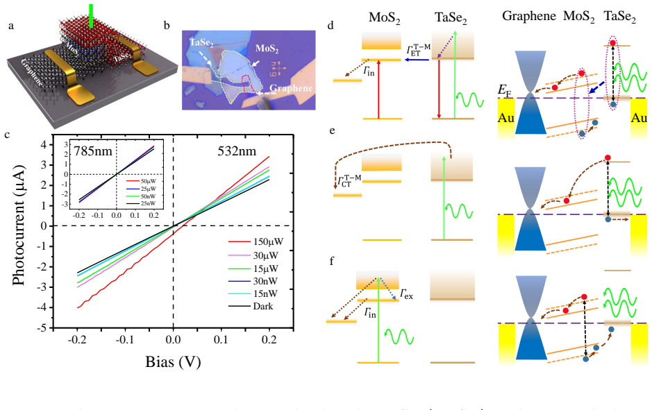
The load-bearing mechanism is the specific band structure of 2H-TaSe2: a narrow charge-density-wave-reconstructed band around the Fermi energy, with a large energy separation to the next bands, gives the material both metallic conductivity and optical inter-band transitions; the parallel-band region between $\Gamma$ and K provides strong absorption, and phonon-assisted relaxation feeds the broad emission. The second mechanism is non-radiative resonant energy transfer: the quasi-two-dimensional in-plane transition dipoles of TaSe2 and MoS2 allow momentum-matched dipole-dipole coupling, described by a rate-equation model whose central parameter is the transfer rate $\Gamma_{ET}$ from TaSe2 to MoS2. The third mechanism is the vertical built-in field in the TaSe2/MoS2/graphene stack, which separates photo-generated carriers and, together with hole trapping in MoS2 gap states, provides photoconductive gain.
What would settle it
Measure the photoluminescence decay of 2H-TaSe2 with a setup whose time resolution is better than 1 picosecond, for example a streak camera or femtosecond upconversion. If the decay time comes out below about 1 ps, the long-lifetime hot-carrier story collapses; a second check is to map photocurrent versus laser-spot-to-contact distance on bare TaSe2 and see whether the decay length matches a diffusion length computed from the true lifetime.
Extended reading notes
Core claim
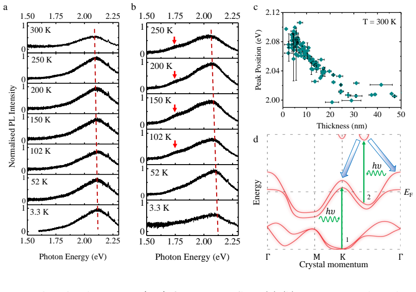
On the paper's own terms, the discovery is that the metallic character of 2H-TaSe2 does not prevent strong inter-band optical transitions. Its band structure has a narrow band at the Fermi energy and well-separated bands above and below; with 2.33 eV excitation, a direct transition at the K point and a parallel-band transition between $\Gamma$ and K both contribute to absorption, and photoexcited carriers relax indirectly with phonon assistance, producing a broad photoluminescence peak near 2.0-2.1 eV rather than the weak emission expected of a conventional metal. The same photoexcited carriers are claimed to survive for picoseconds, long enough to transfer energy by dipole-dipole coupling to MoS2 excitons or to be collected as hot electrons over micrometer distances. The paper then demonstrates that a vertical TaSe2/MoS2/graphene stack turns these effects into a zero-bias photodetector that simultaneously has internal gain and a response up to 0.1 MHz.
Load-bearing premise
The paper's account of long-lived hot carriers depends on measured light-decay times of 2.5 to 6.8 picoseconds, obtained by removing the instrument's own ~95 picosecond response from data that decay almost as fast as the instrument; the paper itself notes that this removal is only trustworthy down to about 9.5 picoseconds, so the real decay could be much faster.
Editorial extensions
If this is right
- 2H-TaSe2 can be used as both electrical contact and light-absorbing layer, so a single material replaces the separate metal electrode and absorber in thin-film optoelectronics.
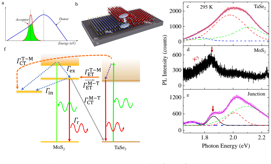
- Because its broad emission overlaps the A-exciton absorption of MoS2, TaSe2 can sensitize multilayer MoS2 by non-radiative energy transfer, brightening an otherwise dark indirect-gap emitter.
- Hot-electron injection from TaSe2 makes it a candidate source for carrier injection into TMDC channels without a conventional metal's short-lived hot carriers.
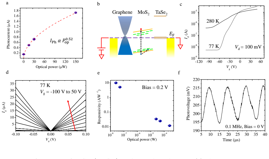
- The vertical TaSe2/MoS2/graphene geometry combines built-in field, short transit time, and trap-assisted gain, enabling zero-bias operation with responsivity above 10 A/W at 0.1 MHz.
Reading between the lines
- Inference: If the true hot-carrier lifetime is below about 1 ps, the micrometer-scale photocurrent observed on bare TaSe2 away from the junction would have to come from something other than long-lived hot electrons, such as lateral carrier diffusion driven by the built-in field or a photothermoelectric current; the paper's zero-bias and 785 nm control experiments narrow this down but cannot fully
- Inference: The same band-separation argument should apply to other 2H polytype metallic TMDCs with charge-density-wave gaps, so the luminescence and energy-transfer effects may be a family property and not unique to TaSe2; testing a sibling compound like 2H-TaS2 would show whether the mechanism generalizes.
- Inference: The thickness-dependent emission peak (about 100 meV shift from monolayer to 50 nm) could be used as an optical ruler for flake thickness in device fabrication, and might allow tuning the donor-acceptor spectral overlap to optimize NRET in heterostructures.
Signed reviews
Editorial analysis
A structured set of objections, weighed in public.
Referee Report
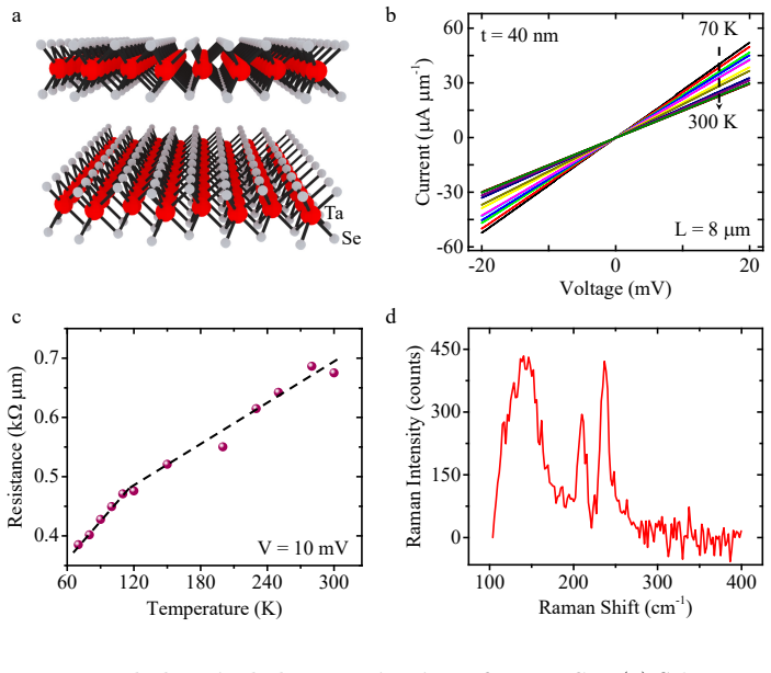
Summary. The paper reports strong photoluminescence and inter-band optical absorption in the layered metal 2H-TaSe2, and uses this in three applications: non-radiative resonant energy transfer (NRET) to enhance MoS2 photoluminescence, hot-electron injection from TaSe2 into MoS2, and a vertical TaSe2/MoS2/graphene photodetector with reported responsivity greater than 10 A/W at 0.1 MHz. The authors characterize the polytype using temperature-dependent resistivity and Raman spectroscopy, rule out oxide-related emission through vacuum, inert-atmosphere, Raman, and stability controls, and present scanning photocurrent, time-resolved photoluminescence, and device-level electrical measurements.
Significance. If the claims are established, the paper demonstrates a multifunctional metallic 2D material that can serve simultaneously as a contact, an absorber, a PL donor, and a hot-carrier source, which would be of genuine interest for all-2D optoelectronics. The paper has real strengths: careful controls for oxide-related emission (Section 2.1 and Supplementary Notes 3-5), polytype identification by multiple techniques, a large set of TRPL statistics across seven flakes, and a vertical photodetector with a useful performance comparison table. These direct measurements are valuable independently of the mechanistic interpretations. However, two load-bearing mechanistic claims—the long hot-electron lifetime and the NRET attribution—rest on evidence that is weaker than the paper's framing suggests, and they need to be re-supported or reframed before publication.
major comments (3)
- [Supplementary Note 7; Section 2.1; Abstract] The paper's central claim that TaSe2 has a 'rather long lifetime' and is an 'excellent hot electron injector' is not supported by the TRPL data. The mean deconvolved lifetimes (6.8 ps at 45 µW and 2.5 ps at 140 µW) are below the authors' own accuracy threshold, stated as 10% of the IRF width (about 9.5 ps for an IRF FWHM of ~95 ps). The Supplementary Note itself concludes that the lifetimes are 'shorter than 10 ps', and the main text acknowledges 'some inaccuracy'. Calling these values 'significantly longer than conventional metals' therefore overstates what the measurement can establish. The authors should either provide a direct measurement with faster time resolution (e.g., a streak camera or upconversion setup) or explicitly downgrade the claim to an upper bound of about 10 ps.
- [Section 2.3, Points 5 and 6 in Figure 4] The off-junction photocurrent observed when the 532 nm laser is on TaSe2 several micrometers away from the contact is attributed to collection of photoexcited carriers over that distance. This is quantitatively difficult to reconcile with a carrier lifetime of at most tens of picoseconds. For a conservative mobility of 100 cm2/Vs and a lifetime of 10 ps, the diffusion length is of order 50 nm, orders of magnitude shorter than the micrometer-scale collection shown in Figure 4b,d. The alternative bolometric or photoconductive response of the TaSe2 channel—which would also be bias-dependent and vanish at zero bias—is not excluded by the 785 nm control, because that control only shows a weaker photoresponse, not the absence of a thermal mechanism. The authors should provide a quantitative carrier-collection model or a discriminating experiment (e.g., temperature dependence of the photocurrent, time-resolved photocurrent, or a study of the photocurrent versus contact distance).
- [Section 2.2, Equation (1) and Supplementary Note 8] The NRET attribution of the sevenfold MoS2 PL enhancement relies on a rate-equation model with several unmeasured rates (Gamma_ET, Gamma_CT, Gamma_s, Gamma_d, and the generation ratio). The model is not fitted to the data, and the derivation assumes that charge transfer, cavity/reflection effects, and changes in MoS2 absorption are negligible. No spacer-layer control (e.g., inserting hBN of varying thickness) is provided to establish the distance-dependent dipole-dipole character of the enhancement. As written, the data show a real PL enhancement but do not uniquely identify the mechanism. Please add a control experiment or explicitly model the alternative contributions.
minor comments (6)
- [Abstract and Section 3] The abstract and discussion state that TaSe2 exhibits a 'rather long lifetime' of photoelectrons, while Supplementary Note 7 concludes that the lifetime is shorter than 10 ps. These statements should be reconciled so the main text does not contradict the supplementary data.
- [Section 2.1] The claim of 'strong optical absorption' is not directly quantified. The differential reflectance data in Supplementary Figure 9 show a broad interference-dominated response with no sharp excitonic feature. An absorption spectrum or a quantitative comparison with a known absorber would strengthen the statement.
- [Figure 2c] The caption states that error bars are obtained from a large number of flakes and positions, but it does not specify whether they are standard deviations or standard errors, nor the number of samples. Please provide this information.
- [Figure 4d] The top panel of Figure 4d is described as the spatial distribution of the built-in field, but it has no axis labels or scale. A quantitative relationship between this schematic field profile and the photocurrent data would help the reader evaluate the argument.
- [Supplementary Note 7] The sentence 'deconvolution can accurately extract lifetimes only up to 10% of the IRF width' should read 'down to 10% of the IRF width'. The extracted values below this threshold are currently reported as means with standard deviations, which suggests a precision the authors themselves disclaim; a clear uncertainty statement is needed.
- [Section 2.4, Figure 6f] The high-speed measurement is performed with a 10 MΩ oscilloscope termination. Please state the RC-limited bandwidth of the measurement chain so that the 0.1 MHz response is not overinterpreted as the intrinsic detector bandwidth.
Circularity Check
No significant circularity: the paper's central claims rest on new measurements, and the rate-equation model is not fitted to the quantity it is used to explain.
full rationale
I examined the derivation chain for the PL enhancement, the hot-electron-lifetime claim, and the photodetector responsivity. The PL enhancement from MoS2 in the TaSe2/MoS2 stack is a directly measured seven-fold change, and the rate-equation model in Supplementary Note 8 (Eqs. 1-4) is a phenomenological description using unmeasured rates; the enhancement factor alpha is not obtained by fitting the model to the enhancement, so Eq. (1) does not reduce to its own input by construction. The hot-electron claim is supported by two independent measurements, TRPL lifetimes and scanning photocurrent, and the paper uses the extracted lifetimes to interpret the photocurrent rather than fitting the photocurrent to define a lifetime. The vertical photodetector responsivity is a measured device result compared against external benchmarks in Supplementary Table 1. The paper cites the authors' prior work (refs 5, 20, 42) for NRET and vertical-device frameworks, but those citations are not load-bearing for the new measurements: the NRET framework is also supported by independent references 17-19, and the central experimental claims do not depend on an unverified self-citation. The TRPL limitation noted in Supplementary Note 7 (deconvolution can extract lifetimes only down to about 10% of the IRF width, while the extracted means are 6.8 ps and 2.5 ps) is a measurement-accuracy caveat, not a circular step, and the paper explicitly acknowledges the resulting inaccuracy. No fitted parameter is renamed as a prediction, no uniqueness theorem is imported from the authors' own work, and no ansatz is smuggled in through self-citation. I therefore find no circularity in the claimed derivation chain.
Assumptions & free parameters
free parameters (1)
- Power-law exponent n =
0.52
assumptions (4)
- ad hoc to paper The PL enhancement of MoS2 on TaSe2 is modeled solely by non-radiative energy transfer rates (Gamma_ET, Gamma_CT, Gamma_s, Gamma_d) without measurable values; other contributions such as charge transfer, cavity or reflection effects, and altered absorption are assumed negligible.
- domain assumption Published band structures and ARPES data for 2H-TaSe2 (refs 11-15, 29-31) are accurate enough to assign the observed PL to specific interband transitions at 2.33 eV.
- domain assumption The deconvolved TRPL lifetimes (2.5-6.8 ps) are treated as physically meaningful carrier lifetimes even though the measured decays are close to the instrument response function and the paper states deconvolution is only reliable to about 10 percent of the IRF width.
- domain assumption The ratio of measured PL intensities (MoS2 on TaSe2 vs on SiO2) is taken directly as the exciton-density enhancement; no correction is made for possible differences in laser absorption, outcoupling, or interference in the stack.
Cite this review
Pith. "Pith review of Light emission from the layered metal 2H-TaSe$_2$ and its potential applications." pith.science (2026). https://pith.science/paper/E6PCVGOL
@misc{pith2026190806913,
  author       = {Pith},
  title        = {Pith review of: Light emission from the layered metal 2H-TaSe$_2$ and its potential applications},
  year         = {2026},
  howpublished = {\url{https://pith.science/paper/E6PCVGOL}},
  note         = {Machine review of arXiv:1908.06913}
}
abstract
Conventional metals, in general, do not exhibit strong photoluminescence. 2H-TaSe$_2$ is a layered transition metal dichalcogenide that possesses metallic property with charge density wave characteristics. Here we show that 2H-TaSe$_2$ exhibits a surprisingly strong optical absorption and photoluminescence resulting from inter-band transitions. We use this perfect combination of electrical and optical properties in several optoelectronic applications. We show a seven-fold enhancement in the photoluminescence intensity of otherwise weakly luminescent multi-layer MoS$_2$ through non-radiative resonant energy transfer from TaSe$_2$ transition dipoles. Using a combination of scanning photocurrent and time-resolved photoluminescence measurements, we also show that the hot electrons generated by light absorption in TaSe$_2$ have a rather long lifetime unlike conventional metals, making TaSe$_2$ an excellent hot electron injector. Finally, we show a vertical TaSe$_2$/MoS$_2$/graphene photodetector demonstrating a responsivity of $>10$ AW$^{-1}$ at $0.1$ MHz - one of the fastest reported photodetectors using MoS$_2$.
Figures
Figures from the paper (3 more)

Reference graph
Works this paper leans on
-
[1]
Atomically thin p–n junctions with van der waals heterointerfaces
Lee, C.H et al. Atomically thin p–n junctions with van der waals heterointerfaces. Nature nanotechnology 9, 676 (2014)
work page 2014
-
[2]
Withers, F. et al. WSe2 light-emitting tunneling transistors with enhanced brightness at room temperature. Nano letters 15, 8223–8228 (2015)
work page 2015
-
[3]
Shim, J. et al. Electronic and optoelectronic devices based on two-dimensional materials: From fabrication to application. Advanced Electronic Materials 3, 1600364 (2017)
work page 2017
-
[4]
Massicotte, M. et al. Picosecond photoresponse in van der waals heterostructures. Nature nanotechnology 11, 42–46 (2016). 14
work page 2016
-
[5]
Kallatt, S., Nair, S. & Majumdar, K. Asymmetrically encapsulated vertical ITO/MoS2/Cu2O photodetector with ultrahigh sensitivity. Small 14, 1702066 (2018)
work page 2018
-
[6]
Withers, F. et al. Light-emitting diodes by band-structure engineering in van der waals heterostructures. Nature materials 14, 301 (2015)
work page 2015
-
[7]
Wilson, J.A., Di Salvo, F.J. & Mahajan, S. Charge-density waves in metallic, layered, transition-metal dichalcogenides. Physical review letters 32, 882 (1974)
work page 1974
- [8]
Show all 59 references
-
[9]
& Tanaka, S
Naito, M. & Tanaka, S. Electrical tranport properties in 2H-NbS 2, -NbSe 2, -TaS 2 and -TaSe2. Journal of the Physical Society of Japan 51, 219–227 (1982)
1982
-
[10]
T., Du, Y., Liu, H
Neal, A. T., Du, Y., Liu, H. & Ye, P. D. Two-dimensional TaSe 2 metallic crystals: spin– orbit scattering length and breakdown current density. Acs Nano 8, 9137–9142 (2014)
2014
-
[11]
& Smith, N.V
Rossnagel, K. & Smith, N.V. Spin-orbit splitting, fermi surface topology, and charge- density-wave gapping in 2H-TaSe2. Physical Review B 76, 073102 (2007)
2007
-
[12]
Laverock, J. et al. k-resolved susceptibility function of 2H-TaSe2 from angle-resolved pho- toemission. Physical Review B 88, 035108 (2013)
2013
-
[13]
Renteria, J. et al. All-metallic electrically gated 2H-TaSe 2 thin-film switches and logic circuits. Journal of Applied Physics 115, 034305 (2014)
2014
-
[14]
Tsoutsou, D. et al. Epitaxial 2d MoSe 2 (HfSe2) semiconductor/2D TaSe 2 metal van der waals heterostructures. ACS applied materials & interfaces 8, 1836–1841 (2016)
2016
-
[15]
Li, Y.W. et al. Folded superstructure and degeneracy-enhanced band gap in the weak- coupling charge density wave system 2H- TaSe 2. Physical Review B 97, 115118 (2018)
2018
-
[16]
Shi, J. et al. Chemical vapor deposition grown wafer-scale 2D Tantalum Diselenide with robust charge-density-wave order. Advanced Materials 30, 1804616 (2018)
2018
-
[17]
Kozawa, D. et al. Evidence for fast interlayer energy transfer in MoSe 2/WS2 heterostruc- tures. Nano letters 16, 4087–4093 (2016). 15
2016
-
[18]
& Demir, H
Guzelturk, B. & Demir, H. V. Near-field energy transfer using nanoemitters for optoelec- tronics. Advanced Functional Materials 26, 8158–8177 (2016)
2016
-
[19]
Deshmukh, R. et al. Long-range resonant energy transfer using optical topological transi- tions in metamaterials. ACS Photonics 5, 2737–2741 (2018)
2018
-
[20]
Dandu, M. et al. Strong single-and two-photon luminescence enhancement by non-radiative energy transfer across layered heterostructure. ACS nano 13, 4795–4803 (2019)
2019
-
[21]
& Mahajan, S
Wilson, J.A., Di Salvo, F.J. & Mahajan, S. Charge-density waves and superlattices in the metallic layered transition metal dichalcogenides. Advances in Physics 24, 117–201 (1975)
1975
-
[22]
& Tanuma, S
Inada, R., ¯Onuki, Y. & Tanuma, S. Hall effect of 1T-TaS 2 and 1T-TaSe2. Physica B+ C 99, 188–192 (1980)
1980
-
[23]
Hajiyev, P., Cong, C., Qiu, C. & Yu, T. Contrast and raman spectroscopy study of single-and few-layered charge density wave material: 2H-TaSe 2. Scientific reports 3, 2593 (2013)
2013
-
[24]
A., Cruz, M
Yan, J. A., Cruz, M. A. D., Cook, B. & Varga, K. Structural, electronic and vibrational properties of few-layer 2H- and 1T-TaSe 2. Scientific reports 5, 16646 (2015)
2015
-
[25]
Luo, H. et al. Differences in chemical doping matter: Superconductivity in Ti 1−xTaxSe2 but not in Ti 1−xNbxSe2. Chemistry of Materials 28, 1927–1935 (2016)
2016
-
[26]
Castellanos-Gomez, A. et al. Fast and reliable identification of atomically thin layers of TaSe2 crystals. Nano Research 6, 191–199 (2013)
2013
-
[27]
& Castellanos-Gomez, A
Coronado, E., Forment-Aliaga, A., Navarro-Moratalla, E., Pinilla-Cienfuegos, E. & Castellanos-Gomez, A. Nanofabrication of TaS 2 conducting layers nanopatterned with Ta2O5 insulating regions via AFM. Journal of Materials Chemistry C 1, 7692–7694 (2013)
2013
-
[28]
Cartamil-Bueno, S. J. et al. High-quality-factor tantalum oxide nanomechanical resonators by laser oxidation of TaSe 2. Nano Research 8, 2842–2849 (2015). 16
2015
-
[29]
Electronic structure of two-dimensional hexagonal diselenides: charge density waves and pseudogap behavior
Kuchinskii, E.Z, Nekrasov, I.A & Sadovskii, M.V. Electronic structure of two-dimensional hexagonal diselenides: charge density waves and pseudogap behavior. Journal of Experi- mental and Theoretical Physics 114, 671–680 (2012)
2012
-
[30]
Band structures of the layer compounds 1T-TaS2 and 2H-TaSe2 in the presence of commensurate charge-density waves
Smith, N.V., Kevan, S.D & Di Salvo, F.J. Band structures of the layer compounds 1T-TaS2 and 2H-TaSe2 in the presence of commensurate charge-density waves. Journal of Physics C: Solid State Physics 18, 3175 (1985)
1985
-
[31]
Jakovidis, G., Riley, J. D. & Leckey, R. C. G. Experimental bandstructure of 2H-TaSe 2. Journal of Electron Spectroscopy and Related Phenomena 61, 19–26 (1992)
1992
-
[32]
Photoluminescence of metals
Mooradian, A. Photoluminescence of metals. Physical Review Letters 22, 185 (1969)
1969
-
[33]
Energy transfer of excitons between quantum wells separated by a wide barrier
Lyo, S.K. Energy transfer of excitons between quantum wells separated by a wide barrier. Physical Review B - Condensed Matter and Materials Physics 62, 13641–13656 (2000)
2000
-
[34]
Bertoni, R. et al. Generation and evolution of spin-, valley-, and layer-polarized excited carriers in inversion-symmetric WSe 2. Physical review letters 117, 277201 (2016)
2016
-
[35]
Puchert, R. P. et al. Spectral focusing of broadband silver electroluminescence in nanoscopic fret-leds. Nature nanotechnology 12, 637 (2017)
2017
-
[36]
Hong, T. et al. Plasmonic hot electron induced photocurrent response at MoS 2–metal junctions. ACS nano 9, 5357–5363 (2015)
2015
-
[37]
Schroder, D. K. Semiconductor material and device characterization (Wiley-Interscience, Hoboken, New Jersey, 2006)
2006
-
[38]
Majumdar, K. et al. STLM: A sidewall tlm structure for accurate extraction of ultralow specific contact resistivity. IEEE Electron Device Letters 34, 1082–1084 (2013)
2013
-
[39]
Photodetectors based on graphene, other two-dimensional materials and hybrid systems
Koppens, F.H.L et al. Photodetectors based on graphene, other two-dimensional materials and hybrid systems. Nature nanotechnology 9, 780 (2014)
2014
-
[40]
Li, X. et al. Graphene and related two-dimensional materials: Structure-property relation- ships for electronics and optoelectronics. Applied Physics Reviews 4, 021306 (2017). 17
2017
-
[41]
Mak, K. F. & Shan, J. Photonics and optoelectronics of 2D semiconductor transition metal dichalcogenides. Nature Photonics 10, 216 (2016)
2016
-
[42]
& Majumdar, K
Murali, K. & Majumdar, K. Self-Powered, Highly Sensitive, High-Speed Photodetection Using ITO/WSe2/SnSe2 Vertical Heterojunction. IEEE Transactions on Electron Devices 65, 4141–4148 (2018)
2018
-
[43]
M., Polyushkin, D
Furchi, M. M., Polyushkin, D. K., Pospischil, A. & Mueller, T. Mechanisms of photocon- ductivity in atomically thin MoS 2. Nano letters 14, 6165–6170 (2014)
2014
-
[44]
Khurgin, J. B. & Sun, G. In search of the elusive lossless metal. Applied Physics Letters 96, 181102 (2010)
2010
-
[45]
Sepia II
Gjerding, M. N., Pandey, M. & Thygesen, K. S. Band structure engineered layered metals for low-loss plasmonics. Nature communications 8, 15133 (2017). Acknowledgements This work was partially supported in part by a grant under Indian Space Research Organi- zation (ISRO), by th...
2017
-
[46]
Castellanos-Gomez, A. et al. Fast and reliable identification of atomically thin layers of TaSe2 crystals. Nano Res. 6, 191–199 (2013)
2013
-
[47]
DecayFit - Fluorescence Decay Analysis Software
Preus, S. DecayFit - Fluorescence Decay Analysis Software. (2014)
2014
-
[48]
Advanced time-correlated single photon counting techniques
Becker, W. Advanced time-correlated single photon counting techniques. 81, (Springer Science & Business Media, 2005)
2005
-
[49]
Xu, Z. et al. Monolayer MoS 2/GaAs heterostructure self -driven photodetector with extremely high detectivity. Nano Energy 23, 89–96 (2016)
2016
-
[50]
Long, M. et al. Broadband Photovoltaic Detectors Based on an Atomically Thin Heterostructure. Nano Lett. 16, 2254–2259 (2016)
2016
-
[51]
Zhang, K. et al. Ultrasensitive Near -Infrared Photodetectors Based on a Graphene - MoTe2-Graphene Vertical van der Waals Heterostructure. ACS Appl. Mater. Interfaces 9, 5392–5398 (2017)
2017
-
[52]
Mudd, G. W. et al. High Broad-Band Photoresponsivity of Mechanically Formed InSe- Graphene van der Waals Heterostructures. Adv. Mater. 27, 3760–3766 (2015)
2015
-
[53]
Yu, W. J. et al. Highly efficient gate -tunable photocurrent generation in vertical heterostructures of layered materials. Nat. Nanotechnol. 8, 952–958 (2013)
2013
-
[54]
Wang, L. et al. MoS2/Si heterojunction with vertically standing layered structure for ultrafast, high-detectivity, self-driven visible-near infrared photodetectors. Adv. Funct. Mater. 25, 2910–2919 (2015)
2015
-
[55]
& Konstantatos, G
Kufer, D. & Konstantatos, G. Highly Sensitive, Encapsulated MoS2 Photodetector with Gate Controllable Gain and Speed. Nano Lett. 15, 7307–7313 (2015)
2015
-
[56]
Qiao, S. et al. A vertically layered MoS2/Si heterojunction for an ultrahigh and ultrafast photoresponse photodetector. J. Mater. Chem. C 6, 3233–3239 (2018)
2018
-
[57]
Chen, Y. et al. High-Performance Photovoltaic Detector Based on MoTe 2/MoS2 Van der Waals Heterostructure. Small 14, 1703293 (2018)
2018
-
[58]
Buscema, M. et al. Fast and broadband photoresponse of few -layer black phosphorus field-effect transistors. Nano Lett. 14, 3347–3352 (2014)
2014
-
[59]
& Majumdar, K
Kallatt, S., Nair, S. & Majumdar, K. Asymmetri cally Encapsulated Vertical ITO/MoS2/Cu2O Photodetector with Ultrahigh Sensitivity. Small 14, 1702066 (2018)
2018
Reviewed August 14, 2026 · model on record in the stance chip above.
Discussion (0). Continue with ORCID to comment.