REVIEW 2 major objections 5 minor 53 references
Single spin-polarised Fermi surface in SrTiO$_3$ thin films
T0 review · 2 major / 5 minor · reviewed 2026-08-14 · deepseek-v4-flash
Pith's one-line read Thin SrTiO3 films grown on niobium-doped substrates reduce the surface 2D electron gas to a single spin-polarised Fermi surface, a configuration that could host Majorana bound states.
desk verdict A credible growth-based route to a single helical Fermi surface on STO, with the Zeeman-gap interpretation still resting on crystal data rather than film data. read the letter →
The pith
A machine-rendered reading of the paper's core claim, the machinery that carries it, and where it could break.
The reading
What carries the argument
The argument rests on two ingredients. The first is a growth-controlled chemical-potential shift: pulsed-laser-deposited homoepitaxial SrTiO3 films on Nb-doped substrates fix the $d_{xy}$ band bottom at 80 meV, far below the 230 meV filling of cleaved or annealed crystals. The second is the Rashba-Zeeman spin gap at the surface Brillouin zone centre, a spin gap that opens at $\bar{\Gamma}$ when spin-orbit and magnetic interactions combine, as previously measured for STO crystal surfaces. Placing the Fermi level inside that gap yields exactly one helical Fermi surface; the simultaneous fit of spin-integrated intensity and the three spin-polarisation components of the momentum distribution curve is the tool that establishes this single band. The Nb-doping level of the substrate moves the band bottom and thus selects how many bands cross the Fermi level.
What would settle it
A decisive test is to measure the spin-resolved dispersion of the 10 u.c. film across a range of binding energies down to the band bottom. If the spin splitting between the two $d_{xy}$ branches is smaller than 80 meV, or if a second spin-polarised branch is found crossing $E_F$, then the Fermi level is not in the Zeeman gap and the central claim is refuted.
Extended reading notes
Core claim
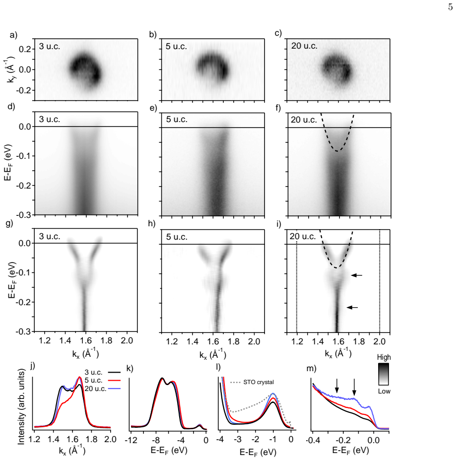
For pulsed-laser-deposited SrTiO3 films between 3 and 20 unit cells (u.c.) thick on 0.5 wt% Nb-doped SrTiO3(001), the surface 2DEG consists of a single $d_{xy}$-derived parabolic band with a band bottom at 80 meV binding energy and an effective mass of $0.74\,m_e$; the heavier $d_{xz}$ and $d_{yz}$ bands are absent, and the state is purely two-dimensional in photon-energy scans. Spin-resolved angle-resolved photoemission on a 10 u.c. film resolves one band whose in-plane spin polarisation is perpendicular to the crystal momentum and reverses sign across the zone centre, matching a helical Rashba-like texture. Interpreting this through the Zeeman gap previously reported at the STO surface Brillouin zone centre, the authors conclude that the Fermi level for these films lies inside the gap, leaving a single spin-polarised Fermi surface. On 0.05 wt% Nb-doped substrates the band bottom moves back up to roughly 170 meV and a second inner band appears to be populated, showing that substrate doping tunes the filling. The authors further infer, from the thickness independence and from XPS of Sr 3d and Ti 3p core levels, that the 2DEG is confined to no more than two unit cells beneath the top TiO2 layer and that the amount of surface SrOx, rather than the Ti3+ fraction, tracks the band filling.
Load-bearing premise
The paper assumes that the magnetic spin gap seen at the surface of SrTiO3 crystals is still present in the thin films and is larger than 80 meV; the authors do not measure this gap in the films and explicitly write that "a change in spin splitting cannot be excluded and requires experimental verification."
Editorial extensions
If this is right
- Stable control of band filling: unlike the universal 230 meV filling seen on cleaved and annealed SrTiO3 crystals, films on Nb-doped substrates put the Fermi level where the experimenter chooses within the spin gap, with no gate voltage or surface contamination required.
- A single helical Fermi surface exists for films of 3 to at least 20 u.c. on 0.5 wt% Nb-doped substrates; combined with the superconductivity of STO, this is a single-material platform for Majorana bound states.
- The 2DEG does not extend beyond the top two unit cells, so its properties are governed by the surface termination and the film's dielectric response rather than the bulk vacancy concentration.
- Changing the substrate Nb doping from 0.5 to 0.05 wt% shifts the band bottom from 80 meV to about 170 meV, showing the filling can be tuned across the spin-gap window.
- The correlation between surface SrOx content and band filling suggests surface chemistry is an additional, possibly independent, tuning knob.
Reading between the lines
- If the Zeeman gap in the films has the same size as on crystals, there should be an intermediate Nb-doping level at which the Fermi level crosses the gap edge; mapping that crossover would turn the single-vs-double Fermi surface transition into a controlled phase boundary.
- Direct SARPES of the full band dispersion, not just the Fermi level, could measure the film's spin splitting directly and test whether the gap is actually larger than the 80 meV band bottom.
- The SrOx correlation suggests a testable extension: preparing adjacent regions of the same film with different SrOx coverage (e.g., by localised annealing or patterned growth) should produce regions with different band fillings on one substrate.
- If the confinement to two unit cells is right, then the single-spiral regime should be independent of film thickness beyond 3 u.c. but disappear when the surface termination is changed to TiO2-rich; this is checkable with existing PLD and ARPES tools.
Signed reviews
Editorial analysis
A structured set of objections, weighed in public.
Referee Report
Summary. The paper reports ARPES and spin-resolved ARPES studies of pulsed-laser-deposited SrTiO3 films grown on Nb-doped SrTiO3(001) substrates. The authors find that the surface 2DEG in these films has a much reduced dxy band filling compared with STO single crystals: the dxy band bottom lies at about 80 meV for films on 0.5 wt% Nb-doped substrates, and the heavy dxz/dyz bands are absent, resulting in a purely two-dimensional state. For these films the Fermi surface consists of a single band with a helical spin texture, which the authors interpret as the Fermi level lying inside the Zeeman gap at the surface Brillouin-zone centre. For films on 0.05 wt% Nb-doped substrates the band filling is larger (about 170 meV), and the authors report evidence for a second populated band. XPS data correlate the band filling with the amount of surface SrOx and suggest that the filling changes are related to the surface termination and possibly the dielectric response. The authors conclude that film growth on Nb-doped substrates provides a stable way to control the 2DEG filling and that the 0.5% films host a single spin-polarised Fermi surface relevant for Majorana physics.
Significance. The experimental data are of high quality and the paper introduces a promising growth-based route to tune the filling of the STO surface 2DEG. The thickness-independence study over 3–20 unit cells, the direct spin-resolved observation of a helical texture in the films, and the XPS correlation with surface SrOx are valuable additions to the field. The paper is also honest about its limitations, explicitly flagging the need for spin-splitting verification. However, the central claim that the Fermi level lies inside the Zeeman gap, and hence that the 0.5% films host a single helical Fermi surface relevant for Majorana physics, depends on an unmeasured parameter: the size (and even existence) of the Zeeman gap in these PLD-grown films is not directly established by the present data. This makes the headline result conditional on an external measurement whose reproducibility is debated.
major comments (2)
- [Section II.A, Fig. 4] The central conclusion that the Fermi level lies inside the Zeeman gap for the 0.5 wt% Nb-substrate films is not directly measured. The spin gap Δ is taken from Ref. [18] on STO single crystals and assumed to be unchanged in the PLD-grown films; the paper itself states in Section II.A that "a change in spin splitting cannot be excluded and requires experimental verification." Because an inner spin-split branch would have a small Fermi wave vector (roughly 0.05 Å⁻¹ for Δ just below 80 meV) and could be masked by the 70 meV energy resolution of the COPHEE SARPES and the strong incoherent spectral weight below 150 meV, the observation of a single band in the spin-resolved MDC does not by itself place the Fermi level inside the gap. This assumption is load-bearing for the Majorana-platform claim in Section III and for the title/abstract statement of a single spin-polarised Fermi surface.
- [Section II.B and Appendix Sec. 5] The evidence that the 0.05 wt% Nb-substrate film hosts two occupied bands relies on a four-peak fit to low-resolution COPHEE data and on unresolved or broad spectral weight in the high-resolution ARPES data; the authors acknowledge in Section II.B that this "requires further investigation." Since this film is one of only two substrate dopings used to demonstrate substrate-controlled band filling, the abstract's claim that band filling "can be controlled" by the substrate doping is stronger than the present evidence. A more systematic doping series or a clearly resolved second band in the 0.05% film would be needed to fully support the claim of controlled, monotonic tuning of the 2DEG filling.
minor comments (5)
- [Fig. 3 caption] The caption describes "The 2DEG on 10 u.c. film grown on highly-doped substrate," but panels (a-c) are for 3, 5, and 20 u.c. films; this appears to be a typo and should be corrected.
- [Appendix Sec. 1] The appendix contains leftover text from a thesis ("6.2. Ba x Sr1°x TiO3 Thin Films" and "6.2.1 Film preparation") that is not part of the paper and should be removed.
- [Sec. II.C] The word "spectromiscroscopy" should be "spectromicroscopy."
- [Appendix Sec. 3] The sentence "Along (a) ΓX and (b) ΓX" should read "Along (a) ΓX and (b) ΓM."
- [Fig. 1] The labels "b) SrTiO3 thin film" and "b) SrTiO3 single crystal" appear to be interchanged; the schematic in panel (b) shows the film structure and should be labelled accordingly.
Circularity Check
No significant circularity: the single-Fermi-surface claim rests on direct ARPES/SARPES data, with the Zeeman-gap interpretation imported from external prior work and explicitly flagged as needing verification.
full rationale
The paper's central claims are direct experimental observations: the dxy band bottom, Fermi wave vector, absence of heavy bands, number of bands crossing EF, and helical spin polarization are all measured by ARPES/SARPES on PLD-grown films. The interpretation that EF lies inside the Zeeman gap combines the measured 80 meV band bottom with the Rashba+Zeeman model from external SARPES on STO crystals (ref. 18), but the gap is not fitted here and is not defined in terms of the conclusion. The authors explicitly acknowledge the assumption: 'a change in spin splitting cannot be excluded and requires experimental verification' (Sec. II A). Ref. 18 is independent, externally falsifiable prior work, even though some authors overlap, and its disputed status is openly discussed (ref. 21, Appendix Sec. 6). No equation in the paper reduces the predicted result to an input by construction, and no fitted parameter is renamed as a prediction. Concerns about the unmeasured Zeeman gap in PLD films are external validity or robustness issues, not circularity.
Assumptions & free parameters
free parameters (3)
- dxy band bottom energy (0.5% films) =
80 meV
- dxy band bottom energy (0.05% films) =
170 meV
- dxy effective mass =
0.74 me
assumptions (4)
- domain assumption The 2DEG on STO films has the same Rashba-Zeeman spin structure as the crystal surface 2DEG, with a Zeeman gap at the zone centre large enough to contain the Fermi level when band filling is 80 meV (from Santander-Syro et al. Nat. Mater. 2014 [18]).
- domain assumption The band filling difference between crystals and films corresponds to a rigid shift of the dxy band, so the spin splitting (Rashba parameter) is unchanged.
- domain assumption Absence of the heavy dxz/dyz bands at hν = 85 eV in films indicates they are unoccupied, not simply not probed.
- domain assumption The similarity of Fermi surfaces for 3, 5, and 20 u.c. films implies the 2DEG is confined to the top 2 u.c. or less.
Cite this review
Pith. "Pith review of Single spin-polarised Fermi surface in SrTiO$_3$ thin films." pith.science (2026). https://pith.science/paper/SYTYQSC2
@misc{pith2026190807379,
  author       = {Pith},
  title        = {Pith review of: Single spin-polarised Fermi surface in SrTiO$_3$ thin films},
  year         = {2026},
  howpublished = {\url{https://pith.science/paper/SYTYQSC2}},
  note         = {Machine review of arXiv:1908.07379}
}
abstract
The 2D electron gas (2DEG) formed at the surface of SrTiO$_3$(001) has attracted great interest because of its fascinating physical properties and potential as a novel electronic platform, but up to now has eluded a comprehensible way to tune its properties. Using angle-resolved photoemission spectroscopy with and without spin detection we here show that the band filling can be controlled by growing thin SrTiO$_3$ films on Nb doped SrTiO$_3$(001) substrates. This results in a single spin-polarised 2D Fermi surface, which bears potential as platform for Majorana physics. Based on our results it can furthermore be concluded that the 2DEG does not extend more than 2 unit cells into the film and that its properties depend on the amount of SrO$_x$ at the surface and possibly the dielectric response of the system.
Figures


Figures from the paper (4 more)


Reference graph
Works this paper leans on
-
[18]
W. Meevasana, P. D. C. King, R. H. He, S.-K. Mo, M. Hashimoto, A. Tamai, P. Songsiriritthigul, F. Baumberger, and Z.-X. Shen, Nature Materials 10, 114 (2011)
work page 2011
-
[1]
Growth of the films 6.2. Ba x Sr1°x TiO3 Thin Films 6.2 Bax Sr1°x TiO3 Thin Films 6.2.1 Film preparation The samples discussed in this sections are all PLD grown films. The growth took place at a substrate temperature of 680± to 700± in an partial oxygen pressure of 1 · 10°5 mbar, same as for the discussed films of BTO and CTO. After growth, the samples are ...
-
[2]
Details of (S)ARPES measurements The prepared films were transferred in-situ to the high-resolution ARPES endstation at the Surface and Interface Spectroscopy beamline of the Swiss Light Source at the Paul Scherrer Institut. X-ray photoemission (XPS) and ARPES spectra were measured with a Scienta R4000 analyzer with instrumental angle and energy resolution...
-
[3]
Dimensionality of the 2DEG In the photon energy scans of the 20 u.c. film shown in Fig. 2 of the main text, the dxy-derived state shows a pure 2D character. This is also concluded for the 3 and 5 u.c. films as noted below. Fig. A2 shows the a the Fermi surface in kx-ky plane for the 5 u.c. film along the symmetry direction GX and FM, which show a pure 2D cha...
-
[4]
ARPES of films on different substrates The larger band filling of the 2DEG on the films grown on the 0.05 wt%, compared to the ones and 0.5 wt% Nb- doped STO(001) substrate, is presented in Fig. 5 of the main text. Here we compare the MDCs and EDCs obtained from these two samples, to show that the data indeed suggests the presence of 2 bands on the film grown ...
-
[5]
SARPES of films on different substrates We now proceed with the comparison of the obtained spin-resolved data. Fig. A4(a) shows the spin-resolved MDC of the 10 u.c. STO/0.5 wt% Nb:STO film, measured at the Fermi level with C + photons of 85 eV, along the ΓY direction, the same as in Fig. 4(c) of the main text. As mentioned, the main spin polarization signal ...
-
[6]
Comparison to conflicting SARPES results Triggered by the SARPES results on STO crystals published in [18], another group has attempted to reproduce these findings under different conditions, but found no clear spin polarization signal [21]. This discrepancy deserves attention, although a full explanation will probably require both further studies and input ...
work page 2012
-
[7]
A8 shows the Sr 3d and Ti 3p XPS spectra of the STO crystal, 20 u.c
Details of the XPS analysis The top panels of Fig. A8 shows the Sr 3d and Ti 3p XPS spectra of the STO crystal, 20 u.c. films on 0.5% Nb:STO and 10 u.c. films on 0.5% Nb:STO, along with their respective fits in the lowe panes. For simplicity, we omitted the fits of spectra of the 3 and 5 u.c. films, which are only shown for comparison as dashed lines in the to...
Show all 53 references
-
[8]
Spaldin, S.-W
N. Spaldin, S.-W. Cheong, and R. Ramesh, Physics Today 63, 38 (2010)
2010
-
[9]
Reyren, S
N. Reyren, S. Thiel, A. D. Caviglia, L. F. Kourkoutis, G. Hammerl, C. Richter, C. W. Schneider, T. Kopp, A.-S. R¨ uetschi, D. Jaccard, M. Gabay, D. A. Muller, J.-M. Triscone, and J. Mannhart, Science 317, 1196 (2007). 16 Intensity (a.u.) Crystal 10 u.c 0.05% 20 u.c. 0.5% Ti 3p...
2007
-
[10]
J. A. Bert, B. Kalisky, C. Bell, M. Kim, Y. Hikita, H. Y. Hwang, and K. A. Moler, Nature Physics 7, 767 (2011)
2011
-
[11]
Ariando, X. Wang, G. Baskaran, Z. Q. Liu, J. Huijben, J. B. Yi, A. Annadi, A. R. Barman, A. Rusydi, S. Dhar, Y. P. Feng, J. Ding, H. Hilgenkamp, and T. Venkatesan, Nature Communications 2, 188 (2011)
2011
-
[12]
Kalisky, J
B. Kalisky, J. A. Bert, C. Bell, Y. Xie, H. K. Sato, M. Hosoda, Y. Hikita, H. Y. Hwang, and K. A. Moler, Nano Letters 12, 4055 (2012)
2012
-
[13]
Ohtomo and H
A. Ohtomo and H. Hwang, Nature 427, 423 (2004)
2004
-
[14]
Cancellieri, M
C. Cancellieri, M. L. Reinle-Schmitt, M. Kobayashi, V. N. Strocov, P. R. Willmott, D. Fontaine, P. Ghosez, A. Filippetti, P. Delugas, and V. Fiorentini, Phys. Rev. B 89, 121412 (2014)
2014
-
[15]
N. C. Plumb and M. Radovi´ c, Journal of Physics: Condensed Matter 29, 433005 (2017)
2017
-
[16]
Frantzeskakis, T
E. Frantzeskakis, T. C. R¨ odel, F. Fortuna, and A. F. Santander-Syro, Journal of Electron Spectroscopy and Related Phenomena 219, 16 (2017)
2017
-
[17]
A. F. Santander-Syro, O. Copie, T. Kondo, F. Fortuna, S. Pailh` es, R. Weht, X. G. Qiu, F. Bertran, A. Nicolaou, A. Taleb- Ibrahimi, P. L. F` evre, G. Herranz, M. Bibes, N. Reyren, Y. Apertet, P. Lecoeur, A. Barth´ el´ emy, and M. J. Rozenberg, Nature 469, 189 (2011)
2011
-
[19]
N. C. Plumb, M. Salluzzo, E. Razzoli, M. M˚ ansson, M. Falub, J. Krempasky, C. E. Matt, J. Chang, M. Schulte, J. Braun, H. Ebert, J. Min´ ar, B. Delley, K.-J. Zhou, T. Schmitt, M. Shi, J. Mesot, L. Patthey, and M. Radovi´ c, Phys. Rev. Lett. 113, 086801 (2014)
2014
-
[20]
S. M. Walker, F. Y. Bruno, Z. Wang, A. de la Torre, S. Ricc´ o, A. Tamai, T. K. Kim, M. Hoesch, M. Shi, M. S. Bahramy, P. D. C. King, and F. Baumberger, Advanced Materials 27, 3894 (2015)
2015
-
[21]
S. N. Rebec, T. Jia, H. M. Sohail, M. Hashimoto, D. Lu, Z.-X. Shen, and R. G. Moore, Proceedings of the National Academy of Sciences 116, 16687 (2019)
2019
-
[22]
Delugas, V
P. Delugas, V. Fiorentini, A. Mattoni, and A. Filippetti, Phys. Rev. B 91, 115315 (2015)
2015
-
[23]
A. D. Caviglia, M. Gabay, S. Gariglio, N. Reyren, C. Cancellieri, and J.-M. Triscone, Physical Review Letters 104, 126803 (2010)
2010
-
[24]
M. J. Veit, R. Arras, B. J. Ramshaw, R. Pentcheva, and Y. Suzuki, Nature Communications 9, 1458 (2018)
2018
-
[25]
A. F. Santander-Syro, F. Fortuna, C. Bareille, T. C. R¨ odel, G. Landolt, N. C. Plumb, J. H. Dil, and M. Radovi´ c, Nature materials 13, 1085 (2014)
2014
-
[26]
L. P. Gor’kov, Journal of Physics: Condensed Matter 27, 252001 (2015)
2015
-
[27]
A. C. Garcia-Castro, M. G. Vergniory, E. Bousquet, and A. H. Romero, Phys. Rev. B 93, 045405 (2016)
2016
-
[28]
McKeown Walker, S
S. McKeown Walker, S. Ricc` o, F. Y. Bruno, A. de la Torre, A. Tamai, E. Golias, A. Varykhalov, D. Marchenko, M. Hoesch, M. S. Bahramy, P. D. C. King, J. S´ anchez-Barriga, and F. Baumberger, Physical Review B 93, 245143 (2016)
2016
-
[29]
Mourik, K
V. Mourik, K. Zuo, S. M. Frolov, S. R. Plissard, E. P. A. M. Bakkers, and L. P. Kouwenhoven, Science 336, 1003 (2012)
2012
-
[30]
J. F. Schooley, W. R. Hosler, and M. L. Cohen, Phys. Rev. Lett. 12, 474 (1964)
1964
-
[31]
Momma and F
K. Momma and F. Izumi, Journal of Applied Crystallography 44, 1272 (2011)
2011
-
[32]
T. C. R¨ odel, F. Fortuna, S. Sengupta, E. Frantzeskakis, P. L. F` evre, F. Bertran, B. Mercey, S. Matzen, G. Agnus, T. Maroutian, P. Lecoeur, and A. F. Santander-Syro, Advanced Materials 28, 1976 (2016)
2016
-
[33]
Z. Wang, S. M. Walker, A. Tamai, Y. Wang, Z. Ristic, F. Y. Bruno, A. De La Torre, S. Ricc` o, N. Plumb, M. Shi, P. Hlawenka, J. S´ anchez-Barriga, A. Varykhalov, T. Kim, M. Hoesch, P. King, W. Meevasana, U. Diebold, J. Mesot, B. Moritz, T. Devereaux, M. Radovi´ c, and F. Baumb...
2016
-
[34]
J. H. Dil, J. W. Kim, S. Gokhale, M. Tallarida, and K. Horn, Phys. Rev. B 70, 045405 (2004)
2004
-
[35]
Ogawa, K
S. Ogawa, K. Kato, N. Nagatsuka, S. Ogura, and K. Fukutani, Phys. Rev. B 96, 085303 (2017)
2017
-
[36]
Zhang, P
P. Zhang, P. Richard, T. Qian, Y.-M. Xu, X. Dai, and H. Ding, Review of Scientific Instruments 82, 043712 (2011)
2011
-
[37]
Moser, L
S. Moser, L. Moreschini, J. Ja´ cimovi´ c, O. S. Bariˇ si´ c, H. Berger, A. Magrez, Y. J. Chang, K. S. Kim, A. Bostwick, E. Rotenberg, L. Forr´ o, and M. Grioni, Phys. Rev. Lett. 110, 196403 (2013)
2013
-
[38]
P. D. C. King, S. McKeown Walker, A. Tamai, A. de la Torre, T. Eknapakul, P. Buaphet, S. K. Mo, W. Meevasana, M. S. Bahramy, and F. Baumberger, Nature Communications 5, 3414 (2014)
2014
-
[39]
Y. S. Kim, J. Kim, S. J. Moon, W. S. Choi, Y. J. Chang, J.-G. Yoon, J. Yu, J.-S. Chung, and T. W. Noh, Applied Physics Letters 94, 202906 (2009)
2009
-
[40]
S. A. Chambers, Y. Du, Z. Zhu, J. Wang, M. J. Wahila, L. F. J. Piper, A. Prakash, J. Yue, B. Jalan, S. R. Spurgeon, D. M. Kepaptsoglou, Q. M. Ramasse, and P. V. Sushko, Phys. Rev. B 97, 245204 (2018)
2018
-
[41]
Hoesch, T
M. Hoesch, T. Greber, V. N. Petrov, M. Muntwiler, M. Hengsberger, W. Auwaerter, and J. Osterwalder, Journal of Electron Spectroscopy and Related Phenomena 124, 263 (2002)
2002
-
[42]
J. H. Dil, Electronic Structure 1, 023001 (2019)
2019
-
[43]
Meier, J
F. Meier, J. H. Dil, and J. Osterwalder, New Journal of Physics 11, 125008 (2009)
2009
-
[44]
R. C. Hatch, K. D. Fredrickson, M. Choi, C. Lin, H. Seo, A. B. Posadas, and A. A. Demkov, Journal of Applied Physics 114, 103710 (2013), https://doi.org/10.1063/1.4821095
2013 doi
-
[45]
Janotti, J
A. Janotti, J. B. Varley, M. Choi, and C. G. Van de Walle, Phys. Rev. B 90, 085202 (2014)
2014
-
[46]
X. Hao, Z. Wang, M. Schmid, U. Diebold, and C. Franchini, Phys. Rev. B 91, 085204 (2015)
2015
-
[47]
Sokolovi´ c, M
I. Sokolovi´ c, M. Schmid, U. Diebold, and M. Setvin, Phys. Rev. Materials 3, 034407 (2019)
2019
-
[48]
Stengel, Phys
M. Stengel, Phys. Rev. Lett. 106, 136803 (2011)
2011
-
[49]
A. A. Sirenko, C. Bernhard, A. Golnik, A. M. Clark, J. Hao, W. Si, and X. X. Xi, Nature 404, 373 (2000)
2000
-
[50]
Ostapchuk, J
T. Ostapchuk, J. Petzelt, V. ˇZelezn´ y, A. Pashkin, J. Pokorn´ y, I. Drbohlav, R. Kuˇ zel, D. Rafaja, B. P. Gorshunov, M. Dressel, C. Ohly, S. Hoffmann-Eifert, and R. Waser, Phys. Rev. B 66, 235406 (2002)
2002
-
[51]
C. Cen, S. Thiel, G. Hammerl, C. Schneider, K. Andersen, C. Hellberg, J. Mannhart, and J. Levy, Nature Materials 7, 298 (2008)
2008
-
[52]
V. N. Petrov, M. S. Galaktionov, and A. S. Kamochkin, Review of Scientific Instruments 72, 3728 (2001)
2001
-
[53]
Yeh and I
J. Yeh and I. Lindau, Atomic Data and Nuclear Data Tables 32, 1 (1985)
1985
Reviewed August 14, 2026 · model on record in the stance chip above.
Discussion (0). Continue with ORCID to comment.