REVIEW 4 major objections 4 minor 39 references
Mottness versus unit-cell doubling as the driver of the insulating state in 1T-TaS2
T0 review · 4 major / 4 minor · reviewed 2026-08-14 · deepseek-v4-flash
Pith's one-line read A single unpaired layer of Star-of-David clusters in 1T-TaS2 holds an odd number of electrons per unit cell yet is insulating, proving Mott localisation alone drives the gap.
desk verdict A genuinely new two-termination STM observation that supports Mott localization in 1T-TaS2, but the conclusion leans on an assumed ACAC stacking and a small number of step-edge examples. read the letter →
The pith
A machine-rendered reading of the paper's core claim, the machinery that carries it, and where it could break.
The reading
What carries the argument
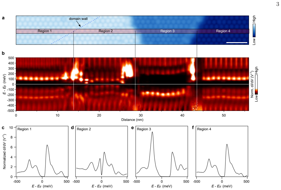
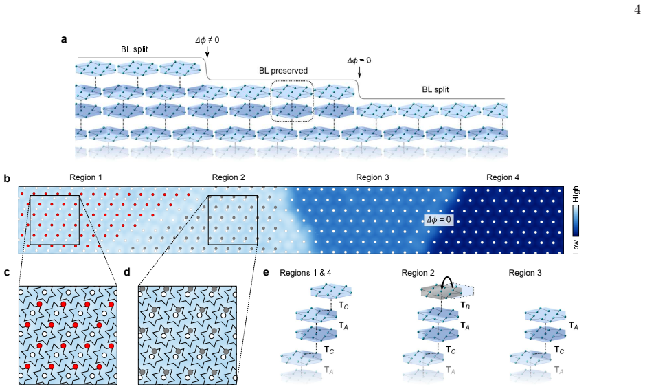
The Star-of-David (SD) cluster is the working object: in the commensurate $\sqrt{13}\times\sqrt{13}\,R13.9^\circ$ charge-density-wave state, each cluster of 13 Ta ions leaves one half-filled orbital, the candidate for Mott localisation. The argument is carried by the two cleavage planes of the ACAC stacking pattern: one plane separates intact $T_A$-stacked bilayers (even electron count per supercell, ~150 meV gap), the other cuts through a bilayer and exposes a single unpaired SD layer (odd electron count, ~50 meV gap). The authors determine which surface is which by measuring the in-plane phase jump of the CDW lattice across single-layer steps — a zero or non-zero shift identifies whether the step ends on the same bilayer or on an unpaired layer. The odd electron count of the unpaired layer is the load-bearing fact that separates the Mott mechanism from unit-cell doubling.
What would settle it
Image the small-gap termination with a structure-sensitive technique: if it shows a reconstruction in which neighbouring Star-of-David clusters pair their remaining orbitals, the surface would have an even number of electrons per unit cell and the ~50 meV gap could be a band gap, not a Mott gap. Alternatively, a magnetic probe that finds no localised $S=1/2$ moments on the unpaired layer would contradict the cluster-Mott interpretation.
Extended reading notes
Core claim
The central claim is that Mott localisation alone is enough to drive the insulating state of 1T-TaS2, and that unit-cell doubling is not needed. From step-terrace spectroscopy combined with an analysis of the in-plane phase of the charge-density-wave lattice across steps, the authors identify two types of surface termination expected for the ACAC stacking pattern: an intact bilayer termination showing a gap of about 150 meV, and an unpaired Star-of-David layer showing a smaller gap of about 50 meV. The unpaired layer has 13 orbitals per surface unit cell, i.e. an odd number of electrons, and it is insulating; this is precisely the situation in which only Mott localisation can produce an insulating state. The authors therefore conclude that the insulating phase of bulk 1T-TaS2 is a cluster Mott insulator, and they interpret the metallic termination, which corresponds to a metastable $T_B$ stacking, as a Mottness-collapsed state in which the effective $U/t$ ratio has been reduced by the interlayer registry.
Load-bearing premise
The conclusion depends on cleaved surfaces preserving the bulk ACAC stacking without reconstruction, so that the small-gap surface really is a single unpaired Star-of-David layer with an odd number of electrons per surface unit cell; if a surface reconstruction re-paired the remaining orbitals, the electron count would become even and a band gap could explain the spectrum.
Editorial extensions
If this is right
- The long-standing cluster-Mott description of 1T-TaS2's low-temperature phase is restored; the insulating state can be understood without invoking unit-cell doubling.
- Proposals of a quantum spin liquid state in 1T-TaS2 remain viable at surfaces and stacking faults, where an unpaired odd-electron layer can host a triangular lattice of localised $S=1/2$ moments.
- Interlayer stacking becomes the microscopic control parameter for insulator-metal transitions in this material, explaining the metallic mosaic, hidden states, and voltage-switching phenomena reported in thin flakes.
- The two measured gaps (~150 meV for the bilayer termination and ~50 meV for the unpaired layer) give concrete targets for cluster-Hubbard-model calculations of the effective $U$ and $t$ parameters.
Reading between the lines
- A monolayer of 1T-TaS2 is by definition an unpaired SD layer, so the data predict that exfoliated or epitaxial monolayers should be insulating with a gap near 50 meV; this is directly testable.
- The difference in gap size between the bilayer (≈150 meV) and unpaired layer (≈50 meV) suggests the effective $U/t$ depends on the stacking environment, so measuring the gap as a function of film thickness or stacking vector would map how correlations respond to dimensionality.
- Controlled tip-induced re-stacking of the top layer onto different stacking vectors ($T_A$, $T_B$, $T_C$) could turn the accidental metallic termination into a deliberate, reversible switch of Mottness — a candidate route for atom-scale memristive devices.
Editorial analysis
A structured set of objections, weighed in public.
Referee Report
Summary. The manuscript reports a low-temperature STM study of 1T-TaS2. The authors identify two distinct surface spectral types: a large-gap (~150 meV) type observed on 18 of 24 cleaved surfaces and a small-gap (~50 meV) type observed on the remaining 6. Using step-terrace topography and analysis of the in-plane phase of the √13×√13 CDW, they assign the large-gap type to termination at the TA-stacked bilayer and the small-gap type to a surface exposing an unpaired Star-of-David layer (TC stacking). They argue that this unpaired layer has an odd number of electrons per surface unit cell and, being insulating, demonstrates that Mott localization alone drives gap formation. They also observe a single metallic region which they attribute to TB stacking, interpreting it as evidence that interlayer stacking controls metal-insulator transitions.
Significance. The paper addresses a key open question in 1T-TaS2: whether the insulating state is a Mott insulator or a band insulator stabilized by unit-cell doubling. The experiment is well conceived: by studying different surface terminations of the same material, it attempts to isolate the layer whose electron count is odd. The step-terrace phase analysis is internally consistent, and the 18:6 distribution of the two spectral types is a large statistical sample at the level of surfaces. The electron-count argument connecting an odd number of electrons per unit cell to the necessity of interactions is textbook and is applied cleanly. If the assignments are correct, the observation of an insulating odd-electron layer would be a direct demonstration that Mott localization is sufficient to open the gap, and the metallic region attributed to TB stacking would be a striking example of stacking-controlled Mottness collapse. However, the strength of these conclusions is currently limited by the lack of independent verification of the ACAC stacking assumption and by the small number of side-by-side observations.
major comments (4)
- [Fig. 2 and p. 2] The central inference that the small-gap termination is an odd-electron Mott insulator depends on two unverified assumptions: (i) the bulk CDW stacking is ACAC, and (ii) the cleaved surface does not reconstruct. The paper states that 'the bulk structure of the CDW should be preserved' (p. 2), but no bulk-sensitive measurement (e.g., X-ray scattering) is presented, and no systematic Fourier-space search for superlattice peaks beyond the √13×√13 CDW is reported for the small-gap surfaces. If the actual stacking differs from ACAC, or if a surface period-doubling re-pairs the nominally unpaired SD orbital, the electron count per surface unit cell could be even, and the ~50 meV gap could be a band or CDW gap rather than a Mott gap. This would invalidate the paper's central claim.
- [Figs. 2–3 and Supplementary Figs. S1–S2] The assignment of the two spectral types to the two ACAC cleavage planes rests on a small number of step-terrace observations: one four-region terrace (Figs. 2–3) with a single partial replication (Supplementary Fig. S2), plus one buried-domain-wall case (Supplementary Fig. S1). The phase-jump analysis is internally consistent, but it presupposes the ACAC model to interpret the displacements; it does not independently establish the stacking. The authors do not report the total number of step edges examined or any instance that would be inconsistent with ACAC. With only two step-edge cases, the possibility of a fortuitous coincidence or of a different stacking sequence (e.g., ABAB or a stacking fault) cannot be excluded.
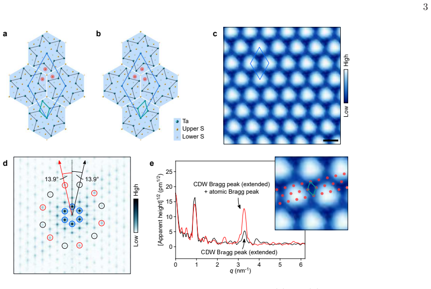
- [p. 4, 'The surface of unpaired SD clusters...'] The paper claims that the unpaired layer has 'an odd number of electrons per (surface) unit cell' (p. 4). This is true only if the surface unit cell equals the √13×√13 cell containing one SD and if the surface layer retains the bulk atomic structure. The STM data do not directly measure the surface electron count, and an in-plane distortion that doubles the surface unit cell (e.g., pairing of SD centers) would make the count even. No such reconstruction is ruled out; the atomic-resolution imaging in Supplementary Fig. S3 is limited to one region and does not establish the absence of long-range period-doubling. Please provide a quantitative check (e.g., analysis of STM topographs for superlattice peaks, or comparison of measured atomic positions to the bulk structure) or state this as a limitation that prevents the Mott conclusion.
- [Fig. 2 and p. 4] The 'Mottness collapse' claim is based on a single observation of a metallic region (Region 2) attributed to TB stacking. The paper explicitly notes that this region was 'observed nowhere else throughout measurements on twenty-three other samples' (p. 3), yet it still makes a general statement that 'the microscopic mechanism of insulator-metal transitions lies in degrees of freedom of interlayer stacking' (Abstract). A single event, with a stacking assignment inferred only from the in-plane displacement, does not support such a broad conclusion. The manuscript should either present additional instances or temper the claim.
minor comments (4)
- [p. 3] The phrase 'twenty-three other samples' appears to be a typo; the paper reports 24 surfaces from 8 crystals, so 'other surfaces' is likely intended.
- [Methods] The normalization of dI/dV data is described, but the resulting uncertainty in the reported gap values (~150 meV and ~50 meV) is not given. A sentence on how gap sizes vary across regions would be useful.
- [Fig. 3e] The schematic in Fig. 3e labels the regions but the caption does not describe the legend, particularly the grey layer for Region 2; please clarify the correspondence.
- [Supplementary Fig. S3] The line cuts in Supplementary Fig. S3(e) are not labeled with the direction convention; adding axis labels would improve interpretability.
Circularity Check
No circularity: the two terminations are identified from STM phase-jump data and prior external stacking models; no fitted parameter is relabeled as a prediction.
full rationale
The paper's derivation is empirical rather than circular. It measures two distinct conductance spectra (a ~150 meV gap on 18 of 24 surfaces and a ~50 meV gap on 6), uses step-edge phase jumps and Fourier analysis to assign them to intact-bilayer versus unpaired-layer terminations under the externally proposed ACAC stacking model, and then applies the standard Mott criterion (odd electron count per unit cell plus insulating behavior) to infer that Mott localization alone drives the gap. No parameter is fitted to a subset of the data and then called a prediction; no equation in the paper reduces to its own input; and the cited prior work by Ritschel et al. and Lee et al. is external to the authors. The ACAC stacking is an assumption, explicitly stated as such ('the bulk structure of the CDW should be preserved'), and the observations are described as 'consistent with' rather than derived from it, so any uncertainty about stacking is a correctness or assumption risk, not a circularity. The self-citations in the Methods are instrumental details and are not load-bearing for the central claim. Thus the central derivation is self-contained with respect to its empirical inputs.
Assumptions & free parameters
assumptions (5)
- domain assumption The bulk CDW of 1T-TaS2 stacks in an alternating TA, TC, TA, TC pattern (ACAC), giving a doubled unit cell.
- domain assumption Each Star-of-David cluster leaves one half-filled Ta 5d orbital at its center, with the other 12 orbitals forming filled bands.
- domain assumption Cleaving preserves the bulk ACAC CDW structure at the surface, with no reconstruction or re-pairing of orbitals.
- domain assumption The number of exposed cleavage planes of the two types is roughly equal, so the observed 18:6 ratio reflects surface formation energies.
- domain assumption The in-plane phase of the CDW, measured by Lawler-Fujita displacement maps and atomic-lattice orientation from Fourier peak intensities, correctly determines interlayer stacking vectors.
Cite this review
Pith. "Pith review of Mottness versus unit-cell doubling as the driver of the insulating state in 1T-TaS2." pith.science (2026). https://pith.science/paper/QW26HLQP
@misc{pith2026190808221,
  author       = {Pith},
  title        = {Pith review of: Mottness versus unit-cell doubling as the driver of the insulating state in 1T-TaS2},
  year         = {2026},
  howpublished = {\url{https://pith.science/paper/QW26HLQP}},
  note         = {Machine review of arXiv:1908.08221}
}
read the original abstract
If a material with an odd number of electrons per unit cell turns out to be insulating, Mott localisation may be invoked as an explanation. This is widely accepted for the layered compound 1T-TaS2, which has a low-temperature insulating phase comprising charge order clusters with 13 unpaired orbitals each. But if the stacking of layers doubles up the unit cell to include an even number of orbitals, the nature of the insulating state is ambiguous. Here, scanning tunnelling microscopy (STM) reveals two distinct terminations of the charge order in 1T-TaS2, the sign of such a double-layer stacking pattern. However, spectroscopy at both terminations allows us to disentangle unit-cell doubling effects and determine that Mott localisation alone is enough to drive gap formation. We also observe the collapse of Mottness at an extrinsically restacked termination, demonstrating that the microscopic mechanism of insulator-metal transitions lies in degrees of freedom of interlayer stacking.
Figures

Figures from the paper (3 more)


Reference graph
Works this paper leans on
-
[1]
Mott, N. F. & Peierls, R. Discussion of the paper by de Boer and Verway. Proc. Phys. Soc. Lond. 49, 72 (1937). https://doi.org/10.1088/0959-5309/49/4S/308
-
[2]
Imada, M., Fujimori, A. & Tokura, Y. Metal-insulator transitions. Rev. Mod. Phys. 70, 1039 (1998). https://doi.org/10.1103/RevModPhys.70.1039
-
[3]
Wilson, J. A., Di Salvo, F. J. & Mahajan, S. Charge-density waves and superlattices in the metallic layered transition metal dichalcogenides. Adv. Phys. 24, 117--201 (1975). https://doi.org/10.1080/00018737500101391
-
[4]
Fazekas, P. & Tosatti, E. Electrical, structural and magnetic properties of pure and doped 1T-TaS _ 2 . Phil. Mag. B 39, 229--244 (1979). https://doi.org/10.1080/13642817908245359
-
[5]
Fazekas, P. & Tosatti, E. Charge carrier localization in pure and doped 1T-TaS _ 2 . Physica B & C 99, 183--187 (1980). https://doi.org/10.1016/0378-4363(80)90229-6
-
[6]
Ritschel, T., Berger, H. & Geck, J. Stacking-driven gap formation in layered 1T-TaS _ 2 . Phys. Rev. B 98, 195134 (2018). https://doi.org/10.1103/PhysRevB.98.195134
-
[7]
Lee, S.-H., Goh, J. S. & Cho, D. Origin of the Insulating Phase and First-Order Metal-Insulator Transition in 1T-TaS _ 2 . Phys. Rev. Lett. 122, 106404 (2019). https://doi.org/10.1103/PhysRevLett.122.106404
-
[8]
Stojchevska, L. et al. Ultrafast switching to a stable hidden quantum state in an electronic crystal. Science 344, 177–180 (2014). https://doi.org/10.1126/science.1241591
Show all 39 references
-
[9]
& Mihailovic, D
Stojchevska, L., Vaskivskyi, I., Mertelj, T., Kusar, P., Svetin, D., Brazovskii, S. & Mihailovic, D. Ultrafast switching to a stable hidden quantum state in an electronic crystal. Science 344, 177–180 (2014)
2014
-
[10]
Hollander, M. J. et al. Electrically Driven Reversible Insulator-Metal Transition in 1T-TaS _ 2 . Nano Lett. 15, 1861--1866 (2015). https://doi.org/10.1021/nl504662b
2015 doi
-
[11]
J., Liu, Y., Lu, W.-J., Li, L.-J., Sun, Y.-P., Robinson, J
Hollander, M. J., Liu, Y., Lu, W.-J., Li, L.-J., Sun, Y.-P., Robinson, J. A. & Datta, S. Electrically Driven Reversible Insulator-Metal Transition in 1T-TaS _ 2 . Nano Lett. 15, 1861--1866 (2015)
2015
-
[12]
Vaskivskyi, I. et al. Controlling the metal-to-insulator relaxation of the metastable hidden quantum state in 1T-TaS _ 2 . Sci. Adv. 1, e1500168 (2015). https://doi.org/10.1126/sciadv.1500168
2015 doi
-
[13]
A., Mertelj, T
Vaskivskyi, I., Gospodaric, J., Brazovskii, S., Svetin, D., Sutar, P., Goreshnik, E., Michailovic, I. A., Mertelj, T. & Mihailovic, D. Controlling the metal-to-insulator relaxation of the metastable hidden quantum state in 1T-TaS _ 2 . Sci. Adv. 1, e1500168 (2015)
2015
-
[14]
Yoshida, M., Suzuki, R., Zhang, Y., Nakano. M. & Iwasa, Y. Memristive phase switching in two-dimensional 1T-TaS _ 2 . Sci. Adv. 1, e1500606 (2015). https://doi.org/10.1126/sciadv.1500606
2015 doi
-
[15]
Vaskivskyi, I. et al. Fast electronic resistance switching involving hidden charge density wave states. Nat. Communs. 7, 11442 (2016). https://doi.org/10.1038/ncomms11442
2016 doi
-
[16]
A., Brazovskii, S., Gospodaric, J., Mertelj, T., Svetin, D., Sutar, P
Vaskivskyi, I., Michailovic, I. A., Brazovskii, S., Gospodaric, J., Mertelj, T., Svetin, D., Sutar, P. & Mihailovic, D. Fast electronic resistance switching involving hidden charge density wave states. Nat. Communs. 7, 11442 (2016)
2016
-
[17]
Cho, D. et al. Nanoscale manipulation of the Mott insulating state coupled to charge order in 1T-TaS _ 2 . Nat. Communs. 7, 10453 (2016). https://doi.org/10.1038/ncomms10453
2016 doi
-
[18]
& Yeom, H.-W
Cho, D., Cheon, S., Kim, K.-S., Lee, S.-H., Cho, Y.-H., Cheong, S.-W. & Yeom, H.-W. Nanoscale manipulation of the Mott insulating state coupled to charge order in 1T-TaS _ 2 . Nat. Communs. 7, 10453 (2016)
2016
-
[19]
Ma, L. et al. A metallic mosaic phase and the origin of Mott-insulating state in 1T-TaS _ 2 . Nat. Communs. 7, 10956 (2016). https://doi.org/10.1038/ncomms10956
2016 doi
-
[20]
Y., Lu, X
Ma, L., Ye, C., Yu. Y., Lu, X. F., Niu, X., Kim, S., Feng, D., Tom\' a nek, D., Son, Y.-W., Chen, X. H. & Zhang, Y. A metallic mosaic phase and the origin of Mott-insulating state in 1T-TaS _ 2 . Nat. Communs. 7, 10956 (2016)
2016
-
[21]
Spin liquids in frustrated magnets
Balents, L. Spin liquids in frustrated magnets. Nature 464, 199--208 (2010). https://doi.org/10.1038/nature08917
2010 doi
-
[22]
Law, K. T. & Lee, P. A. 1T-TaS _ 2 as a quantum spin liquid. Proc. Natl. Acad. Sci. 114 (27), 6996--7000 (2017). https://doi.org/10.1073/pnas.1706769114
2017 doi
-
[23]
Klanj s ek, M. et al. A high-temperature quantum spin liquid with polaron spins. Nat. Phys. 13, 1130--1134 (2017). https://doi.org/10.1038/nphys4212
2017 doi
-
[24]
& Ar c on D
Klanj s ek, M., Zorko, A., Z itko, R., Mravlje, J., Jagli c i\' c , Z., Kumar, P., Prelov s ek, P., Mihailovic, D. & Ar c on D. A high-temperature quantum spin liquid with polaron spins. Nat. Phys. 13, 1130--1134 (2017)
2017
-
[25]
Ribak, A. et al. Gapless excitations in the ground state of 1T-TaS _ 2 . Phys. Rev. B 96, 195131 (2017). https://doi.org/10.1103/PhysRevB.96.195131
2017 doi
-
[26]
Ritschel, T. et al. Orbital textures and charge density waves in transition metal dichalcogenides. Nat. Phys. 11, 328--331 (2015). https://doi.org/10.1038/nphys3267
2015 doi
-
[27]
v., Berger, H., Joe, Y
Ritschel, T., Trinkauf, J., Koepernik, K., B\" u chner, B., Zimmermann, M. v., Berger, H., Joe, Y. I., Abbamonte, P. & Geck, J. Orbital textures and charge density waves in transition metal dichalcogenides. Nat. Phys. 11, 328--331 (2015)
2015
-
[28]
& Tanaka, S
Tanda, S., Sambongi, T., Tani, T. & Tanaka, S. X-Ray Study of Charge Density Wave Structure of 1T-TaS _ 2 . J. Phys. Soc. Jpn. 53, 476--479 (1984). https://doi.org/10.1143/JPSJ.53.476
1984 doi
-
[29]
& Tanaka, S
Naito, M., Nishihara, H. & Tanaka, S. Nuclear quadrupole resonance in the charge density wave state of 1T-TaS _ 2 . J. Phys. Soc. Jpn. 53, 1610--1613 (1984). https://doi.org/10.1143/JPSJ.53.1610
1984 doi
-
[30]
& Tanaka, S
Naito, M., Nishihara, H. & Tanaka, S. Nuclear magnetic resonance and nuclear quadrupole resonance study of ^ 181 Ta in the commensurate charge density wave state of 1T-TaS _ 2 . J. Phys. Soc. Jpn. 55, 2410--2421 (1986). https://doi.org/10.1143/JPSJ.55.2410
1986 doi
-
[31]
Cho, D. et al. Correlated electronic states at domain walls of a Mott-charge-density-wave insulator 1T-TaS _ 2 . Nat. Communs. 8, 392 (2017). https://doi.org/10.1038/s41467-017-00438-2
2017 doi
-
[32]
& Yeom H
Cho, D., Gye, G., Lee, J., Lee, S.-H., Wang, L., Cheong, S.-W. & Yeom H. W. Correlated electronic states at domain walls of a Mott-charge-density-wave insulator 1T-TaS _ 2 . Nat. Communs. 8, 392 (2017)
2017
-
[33]
Qiao, S. et al. Mottness Collapse in 1T-TaS _ 2-x Se _ x Transition-Metal Dichalcogenide: An Interplay between Localized and Itinerant Orbitals. Phys. Rev. X 7, 041054 (2017). https://doi.org/10.1103/PhysRevX.7.041054
2017 doi
-
[34]
& Liu, Z
Qiao, S., Li, X., Wang, N., Ruan, W., Ye, C., Cai, P., Hao, Z., Yao, H., Chen, X., Wu, J., Wang, Y. & Liu, Z. Mottness Collapse in 1T-TaS _ 2-x Se _ x Transition-Metal Dichalcogenide: An Interplay between Localized and Itinerant Orbitals. Phys. Rev. X 7, 041054 (2017)
2017
-
[35]
Ligges, M. et al. Ultrafast Doublon Dynamics in photoexcited 1T-TaS _ 2 . Phys. Rev. Lett. 120, 166401 (2018). https://doi.org/10.1103/PhysRevLett.120.166401
2018 doi
-
[36]
Ligges, M., Avigo, I., Gole z , D., Strand, H. U. R., Beyazit, Y., Hanff, K., Dieknamm, F., Stojchevska, L., Kall\" a ne, M., Zhou, P., Rossnagel, K., Eckstein, M., Werner, P. & Bovensiepen, U. Ultrafast Doublon Dynamics in photoexcited 1T-TaS _ 2 . Phys. Rev. Lett. 120, 166401 (2018)
2018
-
[37]
& Tanaka S
Tani, T., Okajima, K., Itoh, T. & Tanaka S. Electronic transport properties in 1T-TaS _ 2 . Physica B & C 105, 127--131 (1981). https://doi.org/10.1016/0378-4363(81)90230-8
1981 doi
-
[38]
Development of high-field STM and its application to the study on magnetically tuned criticality in Sr _ 3 Ru _ 2 O _ 7
Hanaguri, T. Development of high-field STM and its application to the study on magnetically tuned criticality in Sr _ 3 Ru _ 2 O _ 7 . J. Phys. Conf. Ser. 51, 514 (2006). https://doi.org/10.1088/1742-6596/51/1/117
2006 doi
-
[39]
Lawler M. J. et al. Intra-Unit-Cell Electronic Nematicity of the High-T _ c Copper-Oxide Pseudogap States. Nature 466, 347 (2010). https://doi.org/10.1038/nature09169
2010 doi
Reviewed August 14, 2026 · model on record in the stance chip above.
Discussion (0). Continue with ORCID to comment.