REVIEW 2 major objections 5 minor 14 references
Non-Thermal Resistive Switching in Mott Insulators
T0 review · 2 major / 5 minor · reviewed 2026-08-14 · deepseek-v4-flash
Pith's one-line read In V2O3 nanowires, resistive switching can be driven by an electric field alone, with the wire heating by only 0.3 K.
desk verdict A well-designed experimental study that convincingly separates thermal and non-thermal switching in VO2/V2O3 nanowires; the non-thermal V2O3 conclusion is probably right but rests partly on an unverified thermal-coupling assumption that should be checked. read the letter →
The pith
A machine-rendered reading of the paper's core claim, the machinery that carries it, and where it could break.
The reading
What carries the argument
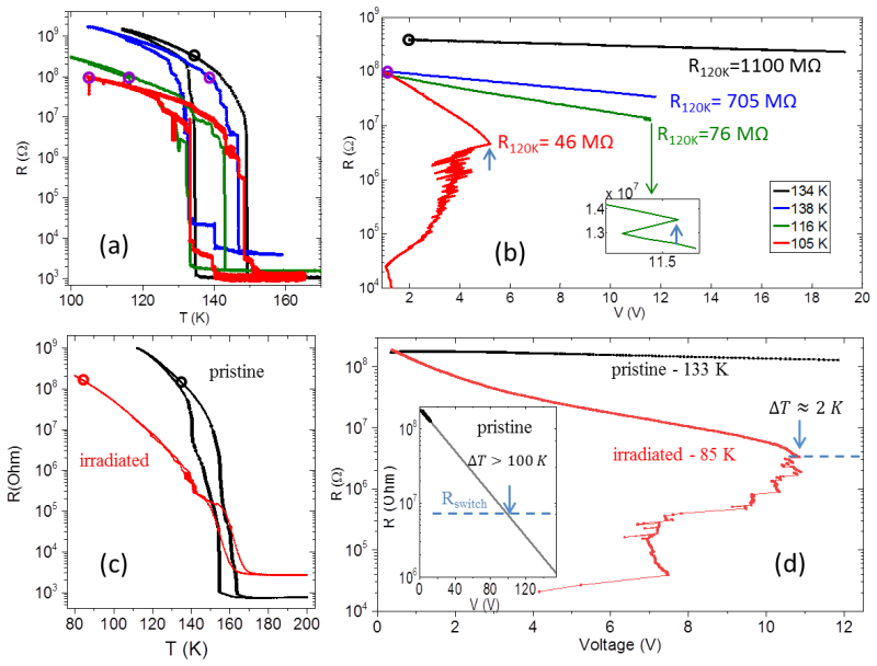
The central measurement object is the quasi-one-dimensional nanowire geometry combined with a measured thermal coupling constant $\kappa$. In steady state the wire temperature is $T_{\mathrm{wire}} = P/\kappa + T_0$ (Eq. 2), with $\kappa$ determined in the fully metallic state; this calibration converts measured $R(P)$ curves into $R(T_{\mathrm{wire}})$ curves and lets the paper test whether switching is purely Joule heating. The transition mechanism itself is field-assisted Poole-Frenkel carrier generation feeding a doping-driven Mott transition: defects create in-gap states that act as a carrier reservoir, the electric field lowers the emission barrier, and dynamical mean-field theory shows that a few percent of extra carriers destroys the insulating state. The nanowire width is comparable to the metal/insulator domain size, which suppresses current filaments and makes the uniform-temperature assumption credible.
What would settle it
Measure the nanowire's temperature directly at the switching event, for example with a local thermometer or scanning thermal probe, while recording the current-voltage curve. If the wire's temperature at switching in V$_2$O$_3$ reaches the equilibrium insulator-metal transition onset near $120$ K, or if the switching resistance falls on the equilibrium $R(T)$ curve when an insulating-state $\kappa$ is used, the non-thermal claim is falsified. A direct reading of $T_{\mathrm{wire}} \approx T_0 + 0.3$ K at the switching point would confirm it.
Extended reading notes
Core claim
The paper's central claim is that an applied electric field can drive a Mott insulator into its metallic state by injecting carriers, not by heating it to its transition temperature. The mechanism is field-assisted excitation of trapped carriers from defect-induced in-gap states into the upper Hubbard band (Poole-Frenkel emission); once the extra carrier density reaches a few percent, the Mott insulator becomes unstable and the gap collapses, so the wire switches at a resistance lower than the equilibrium insulating resistance at any temperature. The paper demonstrates the thermal route in VO$_2$ nanowires and the non-thermal route in V$_2$O$_3$ nanowires, and shows that focused-ion-beam irradiation, which adds defects, turns on the non-thermal route in both materials. Dynamical mean-field calculations for a single-band Hubbard model reproduce the qualitative features: small doping of a few percent suffices, and the switching resistance is weakly temperature dependent.
Load-bearing premise
The load-bearing assumption is that the thermal coupling constant $\kappa$ measured in the fully metallic state also holds in the insulating state and during partial switching; if the true insulating-state $\kappa$ were much smaller, the Joule heating at the switching point could be far larger than the claimed $0.3$ K.
Editorial extensions
If this is right
- The thermal-versus-electronic controversy in VO$_2$ and V$_2$O$_3$ is resolved by sample-specific defect density: low-defect samples switch thermally, high-defect samples switch electronically, which explains contradictory reports on nominally the same material.
- Defect engineering, including focused-ion-beam irradiation, can deliberately select the switching mechanism and make a Mott-insulator device switch with femtojoule-scale energy.
- Non-thermal switching removes the heat-dissipation time bound on device operation, so switching times could approach the picosecond scale seen in optical pump-probe experiments.
- Because the mechanism is generic carrier doping of a Mott state, it should apply broadly across Mott insulators, not just VO$_2$ and V$_2$O$_3$.
- The measured upper bound of 5 fJ per event is about three orders of magnitude below the energy of the Joule-heating route and is comparable to state-of-the-art memristors and biological neurons.
Reading between the lines
- If the doping-driven collapse is correct, then other ways of adding a few percent of carriers, such as chemical doping, electrostatic gating, or photoexcitation, should trigger the same transition at a comparable critical density; the paper does not test this directly.
- A quantitative scaling law linking activation energy and defect density to the switching field could be extracted from a systematic series of irradiation doses; the paper reports the trend but does not formulate such a law.
- The thermal calibration assumption could be checked by measuring $\kappa$ in the insulating state, for example by tracking the wire's transient cooling or by local thermometry; if $\kappa$ is smaller in the insulator, the inferred temperature rise at switching grows, though the resistance-below-equilibrium argument would remain.
- Because the switching energy was only bounded with 6 ns pulses, shorter-pulse experiments could push the true switching energy below 5 fJ and probe the intrinsic speed limit of the electronic route.
Signed reviews
Editorial analysis
A structured set of objections, weighed in public.
Referee Report
Summary. The paper investigates the mechanism of electrically triggered resistive switching in quasi-1D nanowires of VO2 and V2O3. Through power-to-temperature calibration with a single fitting parameter κ, the authors conclude that switching in VO2 is Joule-heating driven, whereas in V2O3 the switching is non-thermal and attributed to field-assisted carrier generation (Poole-Frenkel effect) that dopes the Mott insulator and drives it metallic. They further show that introducing defects via focused ion-beam irradiation enhances the non-thermal switching, report a crossover between thermal and non-thermal regimes controlled by defect density, present DMFT calculations that qualitatively reproduce several observed features under the assumption that field effects act as doping, and demonstrate an ultra-low switching energy of 5 fJ from pulsed measurements. The central claim is that the electrically driven IMT in Mott insulators can be purely field-induced and is universal across materials.
Significance. If the non-thermal switching claim is robust, the paper provides an important resolution to a long-standing controversy and identifies a practical lever (defect engineering) to control the switching mechanism. The use of quasi-1D nanowires to suppress filamentary conduction is a thoughtful design, and the near-constancy of switching power with substrate temperature plus the 5 fJ pulsed-energy measurement are compelling pieces of evidence. The DMFT calculations, however, assume the field-generated-carrier scenario rather than deriving it, so they illustrate but do not independently prove the proposed mechanism. The claim of a universal mechanism for Mott insulators, based on two materials, is plausible but extrapolative.
major comments (2)
- [Power-to-temperature calibration; Fig. 2(c,d); Supplemental Section 3]
- [Introduction; Fig. 3(d)]
minor comments (5)
- [Fig. 1(c) caption]
- [Eq. (2) and following text]
- [Fig. 2(d) and related text]
- [Mechanism section; Supplemental Section 6]
- [References]
Circularity Check
No significant circularity: the non-thermal switching inference rests on an independently calibrated power-to-temperature conversion and an explicitly stated doping assumption, not on a fitted parameter masquerading as a prediction.
full rationale
The paper's central experimental claim for V2O3 is not forced by construction. The thermal coupling constant κ is determined by collapsing metallic-state R(P) curves onto the equilibrium R_eq(T) curve (Fig. 1b–c), and the same κ is then applied without re-fitting to insulating-state data. The subsequent failure of the R(T_wire) curves to collapse onto R_eq(T) in Fig. 2(d) is an empirical result, not an artifact of the calibration. The quoted ΔT ≈ 0.3 K at P ≈ 7 μW is an arithmetic consequence of Eq. (2), T_wire = P/κ + T_0, using a κ measured in the metallic state; the near-constancy of P_switch over a 15 K range of T_0 is an independent, nontrivial check against a thermal picture. The main vulnerability—transferring κ from the metallic to the insulating state—is an assumption, but it is not circular because the target conclusion is not encoded in the calibration. Similarly, the DMFT section explicitly states 'we assume that the main effect of the electric field is to promote charge carriers in the system, which is modeled by shifting the electric (chemical) potential to adjust the doping level.' The calculation therefore illustrates the consequences of that assumption rather than independently deriving field-induced doping. This limits the confirmatory weight of the theory, but the paper does not disguise the assumption, and the experimental voltage/defect trends plus the Poole-Frenkel analysis provide independent evidence for carrier generation. Self-citations appear in support of domain-size simulations and related prior measurements, but no load-bearing uniqueness theorem or hidden ansatz is imported from the authors' own work; no predicted resistance, temperature, or switching threshold is statistically forced by a fitted parameter. The derivation chain is self-contained for the claims actually made, with the acknowledged caveat about κ transferability being a robustness concern rather than circularity.
Assumptions & free parameters
free parameters (4)
- κ (thermal coupling constant) =
21-24 μW/K (V2O3), 45 μW/K (VO2)
- Activation energy Δ (V2O3) =
60 meV
- Activation energy Δ (VO2) =
~265 meV
- U/W ratio in DMFT =
1.7
assumptions (5)
- domain assumption A single thermal coupling constant κ relates dissipated power to nanowire temperature via Twire = P/κ + T0, with uniform temperature in the wire.
- domain assumption κ measured in the metallic state remains valid in the insulating state.
- domain assumption The single-band Hubbard model with U/W=1.7 and semicircular DOS captures the qualitative physics of both VO2 and V2O3.
- ad hoc to paper The main effect of the applied electric field is to promote carriers, equivalent to adjusting the chemical potential (doping level).
- domain assumption The smooth voltage-induced resistance decrease is due to Poole-Frenkel field-assisted excitation of trapped carriers.
Cite this review
Pith. "Pith review of Non-Thermal Resistive Switching in Mott Insulators." pith.science (2026). https://pith.science/paper/IJAOUNQH
@misc{pith2026190808555,
  author       = {Pith},
  title        = {Pith review of: Non-Thermal Resistive Switching in Mott Insulators},
  year         = {2026},
  howpublished = {\url{https://pith.science/paper/IJAOUNQH}},
  note         = {Machine review of arXiv:1908.08555}
}
read the original abstract
Resistive switching can be achieved in a Mott insulator by applying current/voltage, which triggers an insulator-metal transition (IMT). This phenomenon is key for understanding IMT physics and developing novel memory elements and brain-inspired technology. Despite this, the roles of electric field and Joule heating in the switching process remain controversial. We resolve this issue by studying nanowires of two archetypical Mott insulators - VO2 and V2O3. Our findings show a crossover between two qualitatively different regimes. In one, the IMT is driven by Joule heating to the transition temperature, while in the other, field-assisted carrier generation gives rise to a doping driven IMT which is purely non-thermal. By identifying the key material properties governing these phenomena, we propose a universal mechanism for resistive switching in Mott insulators. This understanding enabled us to control the switching mechanism using focused ion-beam irradiation, thereby facilitating an electrically driven non-thermal IMT. The energy consumption associated with the non-thermal IMT is extremely low, rivaling that of state of the art electronics and biological neurons. These findings pave the way towards highly energy-efficient applications of Mott insulators.
Figures

Reference graph
Works this paper leans on
-
[1]
J. Trastoy, Y. Kalcheim, J. del Valle, I. Valmianski, I. K. Schuller, Enhanced metal – insulator transition in V 2O3 by thermal quenching after growth. J. Mater. Sci. 53, 9131– 9137 (2018)
work page 2018
-
[2]
A. Sharoni, J. G. Ram írez, I. K. Schuller, Multiple Avalanches across the Metal -Insulator Transition of Vanadium Oxide Nanoscaled Junctions. Phys. Rev. Lett. 101, 26404 (2008)
work page 2008
-
[3]
A. S. McLeod, E. van Heumen, J. G. Ramirez, S. Wang, T. Saerbeck, S. Guenon, M. Goldflam, L. Ande regg, P. Kelly, A. Mueller, M. K. Liu, I. K. Schuller, D. N. Basov, Nanotextured phase coexistence in the correlated insulator V2O3. Nat. Phys. 13, 80 (2016)
work page 2016
-
[4]
J. Wu, Q. Gu, B. S. Guiton, N. P. de Leon, L. Ouyang, H. Park, Strain -Induced Self Organization of Metal −Insulator Domains in Single -Crystalline VO2 Nanobeams. Nano Lett. 6, 2313–2317 (2006)
work page 2006
-
[5]
J. del Valle, N. Ghazikhanian, Y. Kalcheim, J. Trastoy, M. -H. Lee, M. J. Rozenberg, I. K. 39 Schuller, Resistive asymmetry due to spatial confinement in fir st-order phase transitions. Phys. Rev. B. 98, 45123 (2018)
work page 2018
-
[6]
J. S. Brockman, L. Gao, B. Hughes, C. T. Rettner, M. G. Samant, K. P. Roche, S. S. P. Parkin, Subnanosecond incubation times for electric -field-induced metallization of a correlated electron oxide. Nat. Nanotechnol. 9, 453 (2014)
work page 2014
-
[7]
O. V Lyakh, V. I. Surikov, V. I. Surikov, N. A. Prokudina, Magnetic susceptibility and heat capacity of V2O3 and V1.973Me0.0200O3 (Me = Fe, Cr, and Al). Russ. Phys. J. 55, 116– 119 (2012)
work page 2012
-
[8]
A. Georges, G. Kotlia r, W. Krauth, M. J. Rozenberg, Dynamical mean -field theory of strongly correlated fermion systems and the limit of infinite dimensions. Rev. Mod. Phys. 68, 13–125 (1996)
work page 1996
Show all 14 references
-
[9]
E. Gull, A. J. Millis, A. I. Lichtenstein, A. N. Rubtsov, M. Troyer, P. Werner, Continuous- time Monte Carlo methods for quantum impurity models. Rev. Mod. Phys. 83, 349–404 (2011)
2011
-
[10]
Mazza, A
G. Mazza, A. Amaricci, M. Capone, M. Fabrizio, Electronic transport and dynamics in correlated heterostructures. Phys. Rev. B. 91, 195124 (2015)
2015
-
[11]
Mazza, A
G. Mazza, A. Amaricci, M. Capone, M. Fabrizio, Field -Driven Mott Gap Collapse and Resistive Switch in Correlated Insulators. Phys. Rev. Lett. 117, 176401 (2016)
2016
-
[12]
Kalcheim, N
Y. Kalcheim, N. Butakov, N. M. Vargas, M. -H. Lee, J. del Valle, J. Trastoy, P. Salev, J. Schuller, I. K. Schuller, Robust Coupling between Structural and Electronic Transitions in a Mott Material. Phys. Rev. Lett. 122, 57601 (2019)
2019
-
[13]
Singer, J
A. Singer, J. G. Ramirez, I. Valmianski, D. Cela, N. Hua, R. Kukreja, J. Wingert, O. Kovalchuk, J. M. Glown ia, M. Sikorski, M. Chollet, M. Holt, I. K. Schuller, O. G. Shpyrko, Nonequilibrium Phase Precursors during a Photoexcited Insulator -to-Metal Transition in V2O3. Phys. ...
2018
-
[14]
Abreu, S
E. Abreu, S. Wang, J. G. Ram írez, M. Liu, J. Zhang, K. Geng, I. K. Schuller, R. D. Averitt, Dynamic conductivity scaling in photoexcited V 2O3 thin films. Phys. Rev. B . 92, 85130 (2015). 40
2015
Reviewed August 14, 2026 · model on record in the stance chip above.
Discussion (0). Continue with ORCID to comment.