REVIEW 3 major objections 5 minor 27 references
Electroluminescence and current-voltage measurements of single (In,Ga)N/GaN nanowire light-emitting diodes in the nanowire ensemble
T0 review · 3 major / 5 minor · reviewed 2026-08-14 · deepseek-v4-flash
Pith's one-line read Single-wire electroluminescence probing reveals how many nanowires actually emit in an ensemble LED.
desk verdict A careful single-wire EL/I-V study that delivers a plausible but assumption-laden estimate of active nanowire density; worth refereeing with revisions, not a home run. read the letter →
The pith
A machine-rendered reading of the paper's core claim, the machinery that carries it, and where it could break.
The reading
What carries the argument
The load-bearing identity is $J_{\mathrm{EQE}_{\max}}^{\mathrm{device}} = d_{\mathrm{on}} I_{\mathrm{EQE}_{\max}}^{\mathrm{NW}}$, which equates the ensemble device current density at its relative-EQE maximum with the per-wire current at the single-wire relative-EQE maximum times the number density of emitting nanowires. The relative EQE itself is defined as integrated electroluminescence divided by driving current. Fitting single-wire I-V curves with the modified Shockley equation and using the EQE-maximum current as a common fingerprint lets the authors transfer a single-wire measurement to the ensemble device.
What would settle it
Measure the EQE-versus-current curve of the same individual nanowires before and after depositing the ITO top contact, or count emitting spots in the working device with confocal microscopy: if the single-wire EQE-peak current shifts or the counted active-wire density differs from $6\times10^8$ cm$^{-2}$, the central relation fails.
Extended reading notes
Core claim
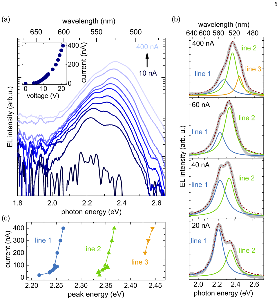
The central claim is that the relative external quantum efficiency of a single nanowire LED peaks at a well-defined current, about 80 nA for wires in this ensemble, and that the same peak appears in the processed ensemble device at a device current density of 47 A/cm$^2$. Dividing the latter by the former gives the number density of emitting nanowires, $d_{\mathrm{on}} = 6\times10^8$ cm$^{-2}$, only about 12% of the as-grown density $5\times10^9$ cm$^{-2}$. Active wires in the working device therefore carry current densities of 20 to 1000 A/cm$^2$ for device current densities of 0.9 to 47 A/cm$^2$. The paper also reports that single-wire EL spectra consist of several quantum-well emission lines whose widths grow as peak energy decreases, and that single-wire I-V curves follow the modified Shockley equation with high ideality factors caused by the probe contact.
Load-bearing premise
The count assumes that the current at which a single nanowire's relative EQE peaks is the same under a tungsten probe contact as for nanowires in the processed device with an ITO top contact, and that current spreads evenly across all active nanowires.
Editorial extensions
If this is right
- The ensemble EQE maximum shifts in proportion to the density of active wires, so a lower active fraction moves the device EQE peak to lower current densities.
- In this sample only about one in eight nanowires emits, meaning the processed LED is far from using its full as-grown wire density and processing optimization has a large headroom.
- Active nanowires in the working device experience current densities of 20 to 1000 A/cm$^2$, one to two orders of magnitude above the naive average over all as-grown wires.
- The ensemble EL spectrum is a superposition of strongly varying single-wire spectra, and single-wire linewidths increase linearly as peak emission energy decreases.
- Reverse leakage observed in the ensemble is also present in single as-grown wires, so it is intrinsic to the nanowire structure rather than a processing artifact.
Reading between the lines
- Beyond the paper: the same EQE-peak ratio could be used as a contact-free process monitor, counting active emitters in any working LED from one representative single-wire calibration.
- Beyond the paper: if the tungsten-probe contact changes the single-wire EQE-peak current, the 12% figure would shift; measuring the same wires through the ITO contact after processing would settle that calibration.
- Beyond the paper: the inferred spread of 20 to 1000 A/cm$^2$ across active wires implies strong current crowding, which could be tested by comparing degradation patterns with the estimated per-wire current density.
- Beyond the paper: the approach could be applied to other self-assembled emitter ensembles, and the per-wire current densities could feed efficiency-droop models that normally rely on device-averaged current density.
Signed reviews
Editorial analysis
A structured set of objections, weighed in public.
Referee Report
Summary. The authors use a tungsten probe tip inside an SEM to contact individual (In,Ga)N/GaN nanowire LEDs in an unprocessed as-grown ensemble and simultaneously measure their EL spectra and I-V characteristics. They observe several emission lines per single-wire spectrum, a linear increase of the spectral FWHM with decreasing emission energy, and diode-like I-V curves that are fitted with a modified Shockley equation, including very high ideality factors attributed to the tungsten/p-GaN contact. The main quantitative result is obtained by comparing the current at which the relative EQE peaks for single nanowires (about 80 nA) with the current density at which the processed ensemble device EQE peaks (47 A/cm2), yielding an active emitting nanowire density of 6e8 cm-2, about 12% of the as-grown density. From this value the authors estimate per-wire current densities of 20-1000 A/cm2 in the working device.
Significance. If the central estimate is correct, the finding that only about one in eight nanowires emits in a processed ensemble LED is important and practically relevant, and the ratio method J_device/I_NW is an elegant, parameter-free way to count active wires. The paper also introduces a useful measurement capability: simultaneous EL and I-V on single nanowires within their native ensemble, avoiding the artifacts of dispersion-based approaches. The authors are transparent about the main assumptions, and the independent cross-check via the ensemble series resistance adds credibility. The significance is tempered, however, by the fact that the headline 12% number depends on two unquantified assumptions: equal current sharing among active wires and transferability of the single-wire EQE-peak current from a tungsten-probe contact to an ITO contact.
major comments (3)
- [Sec. 3, Fig. 6 and the relation J_EQEmax_device = d_on I_EQEmax_NW] The central estimate d_on = 6e8 cm-2 assumes that, at the ensemble EQE peak, every current-carrying nanowire emits and carries exactly I_EQEmax_NW = 80 nA. The paper acknowledges the equal-current condition, but the data in Table 1 show a spread in single-wire series resistances (34-58 MOhm) and threshold voltages (7.0-7.8 V); under a common top contact such variations produce unequal current sharing, so the ensemble EQE is a current-weighted average over shifted single-wire EQE(I) curves rather than N copies of one wire at 80 nA. In addition, the fitted parallel resistance RP ~ 1.5 GOhm per wire implies that even a few nA of leakage through a large fraction of the 5e9 cm-2 wires adds tens of A/cm2 to J_device without contributing to EL, biasing d_on upward. A quantitative sensitivity analysis, such as propagating the measured Rtot and Vth distributions or bounding the leakage contribution, is needed to support the abstract's claim of a 'quite accurate' determination.
- [Sec. 3, Fig. 6(b) and the assumption stated after the definition of relative EQE] The single-wire value I_EQEmax_NW is measured through a tungsten probe that produces ideality factors around 50 and series resistances of tens of MOhm, whereas wires in the processed device are contacted by ITO. The text assumes that a high contact resistance has negligible influence on the integrated EL and relative EQE, but this is not demonstrated and is not obviously guaranteed: a contact-dominated junction can alter the injection geometry, local current density, and heating in the nanowire, and the ITO contact injects over the full nanowire tip. Because d_on is inversely proportional to I_EQEmax_NW, a contact-induced shift of the single-wire EQE peak by even a factor of two changes the headline result. Please provide a direct test, for example measuring the same nanowire under different probe pressures or contact areas, or cross-checking against confocal EL maps of the processed device as in Ref. [7].
- [Sec. 3, Fig. 2 and the paragraph beginning 'Within a set of more than 20 measurement positions'] The assignment of spectra C, E, and G to single nanowires is indirect: the SEM cannot resolve individual wires at a density of 5e9 cm-2, and the single-wire assignment relies on spectral shape and on one supporting example in the supplementary information. If any of these spectra actually contains two or more nanowires, the inferred I_EQEmax_NW is too large and d_on is correspondingly underestimated; the contrast with point F, which is explicitly a bundle and peaks at 300 nA, demonstrates the sensitivity. The paper should state how many of the more than 20 positions were classified as single-wire and provide an estimate of the misclassification rate, or corroborate the assignment with a spatially resolving measurement.
minor comments (5)
- [Sec. 2] The phrase 'we sweeped the voltage' should be 'we swept the voltage'.
- [References] Reference [22] is cited as '[22, ?]' in the text, and the reference list contains a stray '?' and malformed URL prefixes; please clean up the bibliography.
- [Table 1] The table caption contains a typo ('T able 1. . Series resistance'); the column headers could also include the units (Ohm, V) to avoid repetition.
- [Sec. 3, Fig. 4(b)] The FWHM trend is based on ten selected spectra without error bars or a statement of the fitting procedure; please add uncertainty information or soften the linear-trend wording.
- [Sec. 3, inset of Fig. 6(b)] The text says the ensemble relative EQE 'saturates' at 47 A/cm2, while the single-wire EQE is described as having a maximum; please use consistent terminology because the ensemble value is used as the EQE-peak current density.
Circularity Check
No significant circularity: the active-wire density is an inversion of two independently measured EQE-peak quantities, not a fitted or self-defined parameter.
full rationale
The central estimate d_on = J_EQEmax_device / I_EQEmax_NW = 47 A/cm^2 divided by 80 nA, giving about 6e8 cm^-2, is obtained from two independent measurements: the ensemble EQE-peak current density (from the prior device characterization in Ref. [12]) and the single-nanowire EQE-peak current (measured in this paper via probe-tip EL). Neither quantity is derived from the other, and no parameter is fitted to the target density. The relation J_EQEmax_device = d_on * I_EQEmax_NW is an identity under the stated equal-current-sharing assumption; the paper explicitly flags this assumption ('this relation is only true if the NWs have similar contact resistances, resulting in a homogeneous current spreading in the ensemble device') and supports it with the prior ITO-vs-Ni/Au comparison in Ref. [12]. That cited comparison is an external experimental result, not a circular premise. The self-citations to Refs. [7] and [12] supply data, interpretation, and consistency checks, but the 12% estimate does not reduce to those citations by construction. The acknowledged spread in single-wire series resistances and threshold voltages is a quantitative robustness concern, not a circularity. No step in the derivation chain is definitionally equivalent to its input.
Assumptions & free parameters
assumptions (5)
- standard math The modified Shockley equation (Eq. 1), including series resistance and parallel leakage, describes the forward I-V characteristic of the contacted NW diode.
- domain assumption Spectrum C arises from a single contacted NW, inferred from a single dominant asymmetric emission band and behavioral similarity to Ref. [7].
- domain assumption High probe contact resistance does not alter the current dependence of the relative EQE.
- domain assumption All active NWs in the ensemble have the same EQE-peak current and share current homogeneously.
- domain assumption N polarity and the three-dimensional strain profile from Ref. [7] explain the multiple emission lines and their current evolution.
Cite this review
Pith. "Pith review of Electroluminescence and current-voltage measurements of single (In,Ga)N/GaN nanowire light-emitting diodes in the nanowire ensemble." pith.science (2026). https://pith.science/paper/XGFFS6JA
@misc{pith2026190808863,
  author       = {Pith},
  title        = {Pith review of: Electroluminescence and current-voltage measurements of single (In,Ga)N/GaN nanowire light-emitting diodes in the nanowire ensemble},
  year         = {2026},
  howpublished = {\url{https://pith.science/paper/XGFFS6JA}},
  note         = {Machine review of arXiv:1908.08863}
}
read the original abstract
We present the combined analysis of the electroluminescence (EL) as well as the current-voltage (I-V) behavior of single, freestanding (In,Ga)N/GaN nanowire (NW) light-emitting diodes (LEDs) in an unprocessed, self-assembled ensemble grown by molecular beam epitaxy. The data were acquired in a scanning electron microscope equipped with a micromanipulator and a luminescence detection system. Single NW spectra consist of emission lines originating from different quantum wells, and the width of the spectra increases with decreasing peak emission energy. The corresponding I-V characteristics are described well by the modified Shockley equation. The key advantage of this measurement approach is the possibility to correlate the EL intensity of a single NW LED with the actual current density in this NW. This way, the external quantum efficiency (EQE) can be investigated as a function of the current in a single NW LED. The comparison of the EQE characteristic of single NWs and the ensemble device allows a quite accurate determination of the actual number of emitting NWs in the working ensemble LED and the respective current densities in its individual NWs. This information is decisive for a meaningful and comprehensive characterization of a NW ensemble device, rendering the measurement approach employed here a very powerful analysis tool.
Figures


Figures from the paper (3 more)


Reference graph
Works this paper leans on
-
[7]
Musolino M, Tahraoui A, Geelhaar L, Sacconi F, Panetta F, De Santi C, Meneghini M and Zanoni E 2017 Phys. Rev. Appl. 7 044014 ISSN 2331-7019 ( Preprint 1704.01569) URL http://link.aps.org/doi/10.1103/ PhysRevApplied.7.044014
work page Pith review arXiv 2017
-
[1]
Zhao S, Nguyen H P, Kibria M G and Mi Z 2015 Prog. Quantum Electron. 44 14–68 ISSN 00796727 URL http://www.sciencedirect.com/science/article/pii/ S0079672715000403
work page 2015
-
[2]
Kikuchi A, Tada M, Miwa K and Kishino K 2006 Growth and characterization of InGaN/GaN nanocolumn LED Quantum Dots, Part. Nanoclusters III vol 6129 ed Eyink K G and Huffaker D L (SPIE) p 612905 URL http: //link.aip.org/link/?PSI/6129/612905/1
work page 2006
-
[3]
L¨ ahnemann J, Brandt O, Pf¨ uller C, Flissikowski T, Jahn U, Luna E, Hanke M, Knelangen M, Trampert A and Grahn H T 2011 Phys. Rev. B 84 155303 ISSN 1098-0121 URL http://link.aps.org/doi/10.1103/PhysRevB.84. 155303
-
[4]
Bavencove A L, Tourbot G, Garcia J, D´ esi` eres Y, Gilet P, Levy F, Andr´ e B, Gayral B, Daudin B and Dang L S 12 2011 Nanotechnology 22 345705 ISSN 1361-6528 URL http://stacks.iop.org/0957-4484/22/i=34/a=345705
work page 2011
-
[5]
Limbach F, Hauswald C, L¨ ahnemann J, W¨ olz M, Brandt O, Trampert A, Hanke M, Jahn U, Calarco R, Geelhaar L and Riechert H 2012 Nanotechnology 23 465301 ISSN 0957-4484 ( Preprint 1210.7144) URL http: //stacks.iop.org/0957-4484/23/i=46/a=465301?key= crossref.d1856d6f5132f81fefaf90c50a9c1e77
work page Pith review arXiv 2012
-
[6]
Lee Y J, Lee C J, Chen C H, Lu T C and Kuo H C 2011 IEEE J. Sel. Top. Quantum Electron. 17 985–989 ISSN 1077-260X URL http://ieeexplore.ieee.org/lpdocs/ epic03/wrapper.htm?arnumber=5579987
work page 2011
-
[8]
Prague: IMC18 URL http://www.microscopy.cz/proceedings/ all.html
Ledig J, Scholz G, Popp M, Steib F, Fahl A, Wang X, Hartmann J, Mandl M, Schimpke T, Strassburg M, Wehmann H H and Waag A 2014 IMC. Prague: IMC18 URL http://www.microscopy.cz/proceedings/ all.html
work page 2014
Show all 27 references
-
[9]
Growth Des
Albert S, Bengoechea-Encabo A, Ledig J, Schimpke T, S´ anchez-Garcia M a, Strassburg M, Waag A and Calleja E 2015 Cryst. Growth Des. 15 3661–3665 ISSN 1528-7483 URL http://pubs.acs.org/doi/abs/ 10.1021/acs.cgd.5b00235
2015 doi
-
[10]
com/science/electron-and-ion-microscopy/ electro-optical-characterization-3d-leds
Ledig J, F¨ undling S, Steib F, Hartmann J, Wehmann H H and Waag A 2016 Imaging & Mi- croscopy 18 44–49 URL ttp://www.imaging-git. com/science/electron-and-ion-microscopy/ electro-optical-characterization-3d-leds
2016
-
[11]
Hartmann J, Steib F, Zhou H, Ledig J, Nicolai L, Fndling S, Schimpke T, Avramescu A, Varghese T, Trampert A, Straburg M, Lugauer H J, Wehmann H H and Waag A 2017 Journal of Crystal Growth 476 90 – 98 ISSN 0022-0248 URL http://www.sciencedirect.com/ science/article/pii/S0022024...
2017
-
[12]
Musolino M, Tahraoui A, Limbach F, L¨ ahnemann J, Jahn U, Brandt O, Geelhaar L and Riechert H 2014 Appl. Phys. Lett. 105 083505 ISSN 0003- 6951 URL http://scitation.aip.org/content/aip/ journal/apl/105/8/10.1063/1.4894241
2014 doi
-
[13]
5 2287–91 ISSN 1530-6984 URL http: //www.ncbi.nlm.nih.gov/pubmed/16277469
Qian F, Gradeˇ cak S, Li Y, Wen C Y and Lieber C M 2005 Nano Lett. 5 2287–91 ISSN 1530-6984 URL http: //www.ncbi.nlm.nih.gov/pubmed/16277469
2005
-
[14]
W¨ olz M, L¨ ahnemann J, Brandt O, Kaganer V M, Ram- steiner M, Pf¨ uller C, Hauswald C, Huang C N, Geelhaar L and Riechert H 2012 Nanotechnology 23 455203 ISSN 0957-4484 ( Preprint 1210.7597) URL http: //stacks.iop.org/0957-4484/23/i=45/a=455203?key= crossref.00611a10780902ef...
2012 arXiv
-
[15]
Morkoc H 2008 Handbook of Nitride Semiconductors and Devices - Volume 2: Electronic and Optical Processes in Nitrides vol 2 (Wiley-VCH) ISBN 9783527406678
2008
-
[16]
Mohammad S N 2010 J. Appl. Phys. 108 034311 ISSN 00218979 URL http://scitation.aip.org/content/ aip/journal/jap/108/3/10.1063/1.3446845
2010 doi
-
[17]
Suzue K, Mohammad S N, Fan Z F, Kim W, Aktas O, Botchkarev A E and Morkoc H 1996 J. Appl. Phys. 80 4467 ISSN 00218979 URL http://scitation.aip.org/ content/aip/journal/jap/80/8/10.1063/1.363408
1996 doi
-
[18]
Kim J R, Oh H, So H M, Kim J J, Kim J, Lee C J and Lyu S C 2002 Nanotechnology 13 701–704 ISSN 0957-4484
2002
-
[19]
14 2456– 2465 ISSN 1530-6992 URL http://www.ncbi.nlm.nih
Tchernycheva M, Lavenus P, Zhang H, Babichev A V, Jacopin G, Shahmohammadi M, Julien F H, Ciechonski R, Vescovi G and Kryliouk O 2014 Nano Lett. 14 2456– 2465 ISSN 1530-6992 URL http://www.ncbi.nlm.nih. gov/pubmed/24742151
2014
-
[20]
Electron
Brubaker M D, Blanchard P T, Schlager J B, Sanders A W, Herrero A M, Roshko A, Duff S M, Harvey T E, Bright V M, Sanford N A and Bertness K A 2013 J. Electron. Mater. 42 868–874 ISSN 0361-5235 URL http: //link.springer.com/10.1007/s11664-013-2498-y
2013 doi
-
[21]
149 1608–1610 ISSN 00381098 URL http://dx.doi.org/10.1016/j.ssc.2009.06.035
Lin Y, Li Q, Armstrong A and Wang G T 2009 Solid State Commun. 149 1608–1610 ISSN 00381098 URL http://dx.doi.org/10.1016/j.ssc.2009.06.035
2009 doi
-
[22]
Shah J M, Li Y L, Gessmann T and Schubert E F 2003 J. Appl. Phys. 94 2627 ISSN 00218979 URL http://link. aip.org/link/?JAPIAU/94/2627/1
2003
-
[23]
Musolino M, Tahraoui A, van Treeck D, Geel- haar L and Riechert H 2016 Nanotechnol- ogy 27 275203 ISSN 0957-4484 URL http: //stacks.iop.org/0957-4484/27/i=27/a=275203? key=crossref.7ede06cb5905f6299cb25bc59d7fb0da
2016
-
[24]
Musolino M, van Treeck D, Tahraoui A, Scarparo L, De Santi C, Meneghini M, Zanoni E, Geelhaar L and Riechert H 2016 J. Appl. Phys. 119 044502 ISSN 0021-8979 URL http://scitation.aip.org/content/ aip/journal/jap/119/4/10.1063/1.4940949http: //aip.scitation.org/doi/10.1063/1.4940949
2016 doi
-
[25]
Nguyen H P T, Djavid M, Cui K and Mi Z 2012 Nanotechnology 23 194012 ISSN 0957-4484 URL http://www.ncbi.nlm.nih.gov/pubmed/22539212http: //stacks.iop.org/0957-4484/23/i=19/a=194012?key= crossref.72d91a4fb74075e06aa72bd03ef36bd1
2012
-
[26]
Morkoc H 2009 Handbook of Nitride Semiconductors and Devices - Volume 3: GaN-based Optical and Electronic Devices vol 3 (Wiley-VCH) ISBN 9783527406678
2009
-
[27]
16 46164623 ISSN 1530-6984 URL http://pubs
Zhao C, Ng T K, ElAfandy R T, Prabaswara A, Consiglio G B, Ajia I A, Roqan I S, Janjua B, Shen C, Eid J, Alyamani A Y, El-Desouki M M and Ooi B S 2016 Nano Lett. 16 46164623 ISSN 1530-6984 URL http://pubs. acs.org/doi/abs/10.1021/acs.nanolett.6b01945
2016 doi
Reviewed August 14, 2026 · model on record in the stance chip above.
Discussion (0). Continue with ORCID to comment.