REVIEW 3 major objections 5 minor 53 references
Sputtered MoRe SQUID-on-tip for high-field magnetic and thermal nanoimaging
T0 review · 3 major / 5 minor · reviewed 2026-08-14 · deepseek-v4-flash
Pith's one-line read A collimated sputtering source lets SQUID-on-tip magnetic and thermal sensors operate to 5 tesla using the MoRe alloy.
desk verdict A solid fabrication advance with real high-field MoRe SQUIDs-on-tip, but the generality claim rests on an unmeasured ballistic-flow premise. read the letter →
The pith
A machine-rendered reading of the paper's core claim, the machinery that carries it, and where it could break.
The reading
What carries the argument
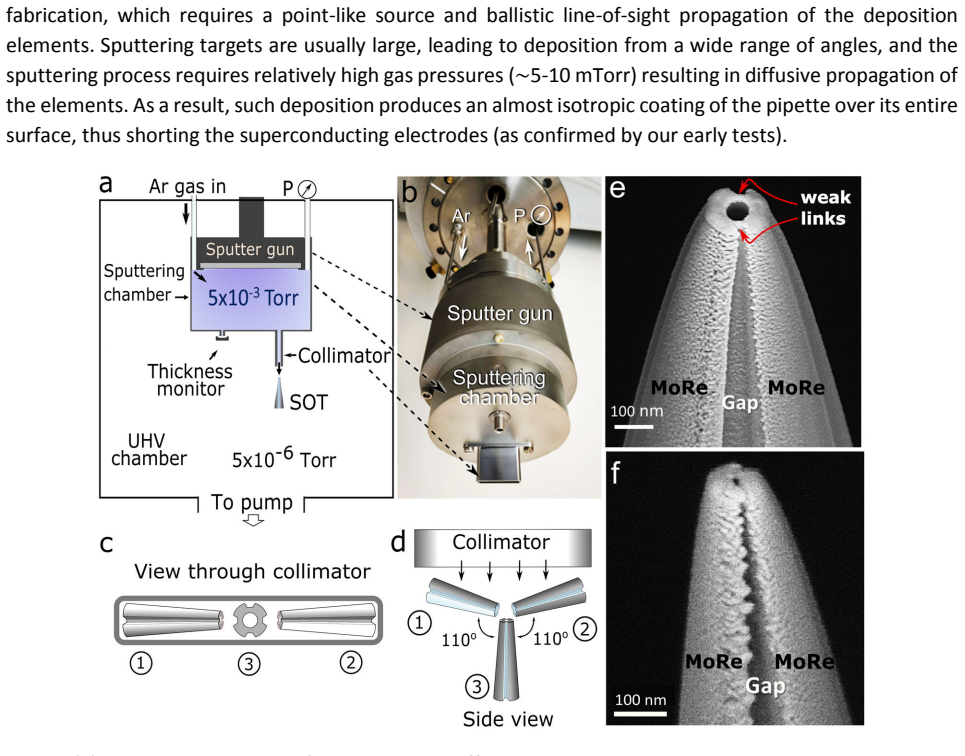
The central mechanism is collimated differential-pressure magnetron sputtering: a commercial magnetron source is sealed inside a small chamber held at roughly 5 mTorr of argon, and a long narrow collimator lets the sputtered flux escape into a UHV chamber at about 5×10⁻⁶ Torr. This produces line-of-sight, approximately point-source deposition that preserves the three-step self-aligned formation of two superconducting leads and an apex loop on a pulled quartz pipette, without lithography, while still allowing standard alloy sputtering recipes to be used.
What would settle it
Deposit MoRe through the same collimator onto a cylindrical test substrate at the same standoff and image the coverage: if the film wraps around the back side or the gap between the two lead depositions closes, the point-source ballistic assumption fails. Alternatively, shorten or widen the collimator while keeping the pressure fixed and check whether the SQUID interference pattern disappears as the deposition becomes more diffuse.
Extended reading notes
Core claim
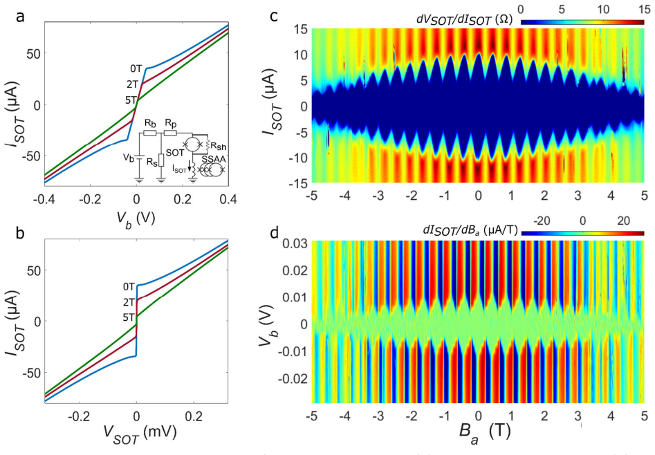
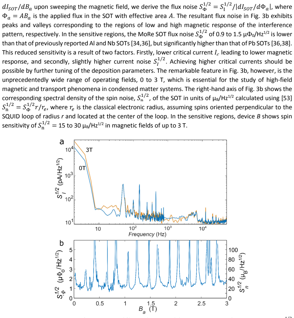
The paper claims that collimated differential-pressure magnetron sputtering enables the self-aligned three-step SQUID-on-tip fabrication from alloy superconductors, a capability previously limited to thermally evaporated elemental metals. In this technique, argon at about 5 mTorr fills a small sputtering chamber, while a 25 mm long, 2×20 mm racetrack collimator lets sputtered atoms pass into a cryopumped chamber at about 5×10⁻⁶ Torr, making the deposition effectively ballistic from a narrow source. Using this method, MoRe SQUID-on-tips with effective diameters of 49 to 105 nm remain superconducting at 5 T, show clear SQUID interference oscillations up to about 3 T with flux noise of 0.9 to 1.5 µΦ₀/√Hz and spin noise of 15 to 30 µB/√Hz, and reach thermal sensitivity better than 4 µK/√Hz over the full range up to 5 T.
Load-bearing premise
The entire fabrication scheme rests on the unmeasured assumption that sputtered atoms travel ballistically through the collimator from a small source, so the three angled depositions leave two separated leads and an apex loop instead of coating the pipette uniformly.
Editorial extensions
If this is right
- SQUID-on-tip sensors can now be made from high-field alloy superconductors, with MoRe operating to 5 T, roughly five times the field range of previous Pb and Nb devices.
- Nanoscale magnetic and spin imaging with sub-50 nm resolution becomes possible in fields up to about 3 T, with spin noise below 30 µB/√Hz in sensitive field regions.
- Cryogenic thermal imaging of dissipation reaches fields up to 5 T with thermal noise below 4 µK/√Hz, enabling studies of dissipation in fractional quantum Hall states and other high-field quantum systems.
- The sputtering route opens the door to other superconducting materials and multilayer structures, potentially tuning critical temperature, critical field, and device functionality beyond what elemental thermal evaporation allowed.
Reading between the lines
- The same differential-pressure collimation concept could transfer to other point-source deposition tasks, such as shadow-masked contacts or nanowire devices, wherever the source pressure and substrate pressure need to be decoupled.
- Because MoRe is not the highest-field superconductor available by sputtering, NbN or MgB2 SQUID-on-tips made this way might operate beyond 5 T, though film stress, oxidation, and deposition temperature would need to be managed.
- The paper observes that MoRe flux noise is higher than Pb SQUID-on-tips and attributes it to lower critical current; a direct next test is whether tuning sputtering parameters or annealing raises Ic and proportionally lowers flux noise.
- If the ballistic-deposition picture is correct, the collimator geometry should produce a sharp angular cutoff, so varying the collimator length or aspect ratio should predictably change the lead gap and interference visibility.
Signed reviews
Editorial analysis
A structured set of objections, weighed in public.
Referee Report
Summary. This manuscript reports a collimated differential-pressure magnetron sputtering method for fabricating SQUID-on-tip (SOT) nanodevices from superconducting alloys, and demonstrates MoRe SOTs with effective diameters down to 49 nm. The devices are characterized by current-voltage curves and SQUID interference patterns up to 5 T at 4.2 K, current-noise spectra, magnetic response functions, and temperature-dependent IVs. The authors report flux noise of 0.9-1.5 micro-Phi0/Hz^1/2 in sensitive field regions up to 3 T and thermal noise better than 4 micro-K/Hz^1/2 up to 5 T, and argue that the technique extends self-aligned SOT fabrication to a broad range of alloys.
Significance. If the fabrication claim holds, this is a practical advance: it replaces thermal evaporation with magnetron sputtering, which is compatible with many superconducting alloys, and the demonstrated MoRe SOTs operate at fields up to 5 T, far beyond the ~1 T range of earlier Pb and Nb SOTs, while retaining thermal sensitivity comparable to Pb SOTs at low field. The device-level evidence is strong: directly measured IV characteristics, SQUID oscillations persisting to 5 T, current-noise spectra, and temperature-dependent IV curves. The sensitivity numbers are derived from directly measured quantities (current noise with separately measured dI/dB or dI/dT) using standard formulas rather than from an unconstrained model. The principal weaknesses are that the general-extension claim rests on an unverified ballistic point-source assumption, and the headline sensitivity statements in the abstract are more sweeping than the data in Figs. 3 and 4.
major comments (3)
- [Fabrication setup (Fig. 1) and Conclusions] The claim that the collimated differential-pressure sputtering scheme provides a point-like ballistic source is not directly established. The stated parameters (~5 mTorr Ar in the sputtering chamber, a 25 mm collimator, and a ~20 mm source-substrate distance) imply a mean free path of order 1 cm, comparable to the collimator length, so transport through the collimator is not trivially ballistic. The SEM gap in Figs. 1e,f is consistent with ballistic deposition but can also be produced by topographic shadowing from the grooved quartz pipette even with a broad angular source, so it does not uniquely prove a point-like source. Because the Conclusions generalize the method to a wide range of materials and multilayer structures, this premise is load-bearing. I request a direct measurement of the angular distribution (for example, film thickness on planar witness substrates through apertures at controlled angles, or sidewall coverage on ungrooved test pipettes), together with a quantitative estimate of the scattering mean free path under the stated conditions. The unpublished early tests with conventional sputtering, cited as 'confirmed by our early tests', should also be shown or described quantitatively.
- [Abstract and Fig. 3b] The flux-sensitivity claim in the abstract, 'flux sensitivity of 1.2 micro-Phi0/Hz^1/2 up to 3 T', is only demonstrated in the sensitive regions of the interference pattern, not over the whole 0-3 T range. Figure 3b shows flux noise oscillating, with values of 0.9-1.5 micro-Phi0/Hz^1/2 in the valleys and substantially higher values near the peaks. The body text already contains the qualifier 'in the sensitive regions', but the abstract and conclusion do not, which overstates the continuous operating specification. In addition, the quoted range appears to be derived from a single device (device B) with no error bars or device-to-device statistics. Please either add the qualifier in the abstract and conclusion or provide a statistical summary over several devices, including the fraction of the 0-3 T range over which the specified sensitivity is maintained.
- [Fig. 4 and Abstract] The thermal-sensitivity statement 'better than 4 micro-K/Hz^1/2 up to 5 T' is supported by device E alone (2.5-3.8 micro-K/Hz^1/2 over the full range), whereas device D, the other device used for the field dependence, reaches about 1 micro-K/Hz^1/2 only up to about 1 T and then exhibits oscillatory behavior, with the 'better than 2 micro-K/Hz^1/2' property restricted to sensitive field regions up to 4 T. The abstract and conclusion should identify which device and which bias-optimization procedure support each quoted specification. The phrase 'about five times higher than any previous report' is also ambiguous: it should specify the benchmark device and the field at which the comparison is made, since the zero-field thermal noise of ~1 micro-K/Hz^1/2 is comparable to, not five times better than, previously reported Pb SOT values [40,41].
minor comments (5)
- [p. 4, film characterization] The statement that 'the critical magnetic field Hc2 of the MoRe being over 5 T' is inferred from the persistence of a critical current at 5 T; a direct measurement or reference for the Hc2 of the deposited MoRe films would be more rigorous.
- [Throughout] Several symbols are garbled in the rendered text (notably the effective-diameter formula and the flux-noise equation); the typesetting should be checked carefully before publication.
- [Fig. 2 caption] The figure captions should state explicitly which devices were annealed and which were not, since annealing is reported to affect the critical current and film quality.
- [References] Reference [42] is cited as 'Nature in press' with an arXiv identifier; this should be updated at proof stage.
- [Fig. 1f] The claim of a 'clear gap' in the 49 nm SOT would be easier to assess with a higher-magnification image or scale-bar overlay; the current image shows limited contrast in the apex region.
Circularity Check
No significant circularity: the reported sensitivities are direct measurements and prior SOT work is used only as benchmarks, not as inputs.
full rationale
The central claims rest on direct electrical and noise measurements, not on a fitted parameter relabeled as a prediction. Current noise is measured directly (Fig. 3a); flux noise is derived by dividing the measured current noise by the measured magnetic response dI/dPhi, with the effective loop area calibrated independently from the field periodicity of the SQUID interference pattern (Fig. 2c). Spin sensitivity uses the standard published Ketchen formula with explicitly stated assumptions about spin position and orientation, and thermal sensitivity is the ratio of measured current noise to measured dI/dT (Fig. 4b). None of these quantities is defined in terms of the paper's claimed conclusion, and no fitted input is renamed as a predicted outcome. Prior SQUID-on-tip works by the same group appear as benchmarks ('comparable to the state-of-the-art Pb SOT devices', 'lower than that of previously reported Al and Nb SOTs'), which is comparison rather than load-bearing derivation. The inference that sputtered atoms propagate ballistically is an empirical interpretation of the observed sharp SEM gap and SQUID interference, not a circular reduction: even if that inference is underdetermined or too strong, it does not make any measured sensitivity equal to an input by construction. No self-definitional relation, fitted-input-as-prediction, author-imported uniqueness theorem, or ansatz-smuggling-via-citation was found. The paper is self-contained against external benchmark comparisons, so the appropriate circularity score is 0.
Assumptions & free parameters
free parameters (1)
- SOT bias voltage V_g =
0.02 V for flux noise (device B), 0.04 V for thermal response (device C), tuned at each field for devices D/E
assumptions (5)
- standard math The SQUID critical current is periodic in applied flux with period Phi0 = h/2e, and the effective loop diameter is inferred from the field periodicity via D = 2 sqrt(Phi0 / (pi Delta B)).
- domain assumption At the stated pressures (about 5 mTorr in the sputtering chamber and about 5e-6 Torr in the UHV chamber), sputtered atoms travel ballistically through the collimator and do not coat the pipette sidewalls.
- domain assumption The spin-noise conversion formula from Ketchen et al. [53] describes a spin located at the loop center and oriented perpendicular to the loop plane.
- domain assumption A resistively shunted SOT behaves as an overdamped SQUID whose current-voltage characteristics and differential resistance encode the magnetic interference pattern without significant thermal or field-induced artifacts.
- domain assumption The thermal response dI_SOT/dT extracted from bath-temperature sweeps from 4.2 to 7 K accurately represents the local temperature response during nanoscale thermal imaging, including at fields above the 0-2 T range checked on one device.
Cite this review
Pith. "Pith review of Sputtered MoRe SQUID-on-tip for high-field magnetic and thermal nanoimaging." pith.science (2026). https://pith.science/paper/3FV6A3H7
@misc{pith2026190809305,
  author       = {Pith},
  title        = {Pith review of: Sputtered MoRe SQUID-on-tip for high-field magnetic and thermal nanoimaging},
  year         = {2026},
  howpublished = {\url{https://pith.science/paper/3FV6A3H7}},
  note         = {Machine review of arXiv:1908.09305}
}
abstract
Scanning nanoscale superconducting quantum interference devices (SQUIDs) are gaining interest as highly sensitive microscopic magnetic and thermal characterization tools of quantum and topological states of matter and devices. Here we introduce a novel technique of collimated differential-pressure magnetron sputtering for versatile self aligned fabrication of SQUID on tip (SOT) nanodevices, which cannot be produced by conventional sputtering methods due to their diffusive, rather than the required directional point-source, deposition. The new technique provides access to a broad range of superconducting materials and alloys beyond the elemental superconductors employed in the existing thermal deposition methods, opening the route to greatly enhanced SOT characteristics and functionalities. Utilizing this method, we have developed MoRe SOT devices with sub-50 nm diameter, magnetic flux sensitivity of 1.2 $\mu\Phi_0/Hz^{1/2}$ up to 3 T at 4.2 K, and thermal sensitivity better than 4 $\mu K/Hz^{1/2}$ up to 5 T, about five times higher than any previous report, paving the way to nanoscale imaging of magnetic and spintronic phenomena and of dissipation mechanisms in previously inaccessible quantum states of matter.
Figures
Figures from the paper (1 more)

Reference graph
Works this paper leans on
-
[1]
M. José Martínez-Pérez and D. Koelle, ''NanoSQUI Ds: Basics and recent advances'', Phys. Sci. Rev. 2, 5001 (2017)
work page 2017
-
[2]
C. Granata and A. Vettoliere, ''Nano Superconduc ting Quantum Interference device: A powerful tool for nanoscale investigations'', Phys. Rep. 614 , 1 (2016)
work page 2016
-
[3]
J. R. Kirtley, L. Paulius, A. J. Rosenberg, J. C . Palmstrom, C. M. Holland, E. M. Spanton, D. Schiessl, C. L. Jermain, J. Gibbons, Y.-K.-K. Fung, M. E. Huber, D. C. Ralph, M. B. Ketchen, G. W. Gibson, and K. A. Moler, ''Scanning SQUID susceptometers with sub-micron spatial resolution'', Rev. Sci. Instrum. 87 , 093702 (2016)
work page 2016
-
[4]
J. R. Kirtley, ''Fundamental studies of supercon ductors using scanning magnetic imaging'', Reports Prog. Phys. 73, 126501 (2010)
work page 2010
-
[5]
R. Kleiner, D. Koelle, F. Ludwig, and J. Clarke, ''Superconducting quantum interference devices: State of the art and applications'', Proc. IEEE 92 , 1534 (2004)
work page 2004
-
[6]
R. L. Fagaly, ''Superconducting quantum interfer ence device instruments and applications'', Rev. Sci. Instrum. 77 , 101101 (2006)
work page 2006
- [7]
- [8]
Show all 53 references
-
[9]
J. R. Kirtley and J. P. Wikswo, ''Scanning SQUID microscopy'', Annu. Rev. Mater. Sci. 29 , 117 (1999)
1999
-
[10]
J. R. Kirtley, C. C. Tsuei, Ariando, C. J. M. V erwijs, S. Harkema, and H. Hilgenkamp, ''Angle-resolved phase-sensitive determination of the in-plane gap symmetry in YBa2Cu3O7−δ'', Nat. Phys. 2, 190 (2006)
2006
-
[11]
D. J. Hykel, C. Paulsen, D. Aoki, J. R. Kirtley , and K. Hasselbach, ''Magnetic fields above the superconducting ferromagnet UCoGe'', Phys. Rev. B 90 , 184501 (2014)
2014
-
[12]
Nishio, V
T. Nishio, V. H. Dao, Q. Chen, L. F. Chibotaru, K. Kadowaki, and V. V. Moshchalkov, ''Scanning SQUID microscopy of vortex clusters in multiband superconductors'', Phys. Rev. B 81 , 020506 (2010)
2010
-
[13]
Kokubo, S
N. Kokubo, S. Okayasu, A. Kanda, and B. Shinoza ki, ''Scanning SQUID microscope study of vortex polygons and shells in weak-pinning disks of an amorphous superconducting film'', Phys. Rev. B 82 , 014501 (2010)
2010
-
[14]
Embon, Y
L. Embon, Y. Anahory, A. Suhov, D. Halbertal, J . Cuppens, A. Yakovenko, A. Uri, Y. Myasoedov, M. L. Rappaport, M. E. Huber, A. Gurevich, and E. Zeldov, ''Probing dynamics and pinning of single vortices in superconductors at nanometer scales'', Sci. Rep. 5, 7598 (2015)
2015
-
[15]
F. S. Wells, A. V. Pan, X. R. Wang, S. A. Fedos eev, and H. Hilgenkamp, ''Analysis of low-field isotropic vortex glass containing vortex groups in YBa2Cu3O7−x thin films visualized by scanning SQUID microscopy'', Sci. Rep. 5, 8677 (2015)
2015
-
[16]
Embon, Y
L. Embon, Y. Anahory, Ž. L. Jelić, E. O. Lachman , Y. Myasoedov, M. E. Huber, G. P. Mikitik, A. V. Silhanek, M. V. Milošević, A. Gurevich, and E. Zeldov, ''Imaging of super-fast dynamics and flow instabilities of superconducting vortices'', Nat. Commun. 8, 85 (2017)
2017
-
[17]
J. A. Bert, B. Kalisky, C. Bell, M. Kim, Y. Hik ita, H. Y. Hwang, and K. A. Moler, ''Direct imaging of the coexistence of ferromagnetism and superconductivity at the LaAlO3/SrTiO3 interface'', Nat. Phys. 7, 767 (2011)
2011
-
[18]
Kalisky, E
B. Kalisky, E. M. Spanton, H. Noad, J. R. Kirtl ey, K. C. Nowack, C. Bell, H. K. Sato, M. Hosoda, Y. Xie, Y. Hikita, C. Woltmann, G. Pfanzelt, R. Jany, C. Richter, H. Y. Hwang, J. Mannhart, and K. A. Moler, ''Locally enhanced conductivity due to the tetragonal domain structure...
2013
-
[19]
X. R. Wang, C. J. Li, W. M. Lu, T. R. Paudel, D . P. Leusink, M. Hoek, N. Poccia, A. Vailionis, T. Venkatesan, J. M. D. Coey, E. Y. Tsymbal, Ariando, and H. Hilgenkamp, ''Imaging and control of ferromagnetism in LaMnO3/SrTiO3 heterostructures'', Science 349 , 716 (2015)
2015
-
[20]
Anahory, L
Y. Anahory, L. Embon, C. J. Li, S. Banerjee, A. Meltzer, H. R. Naren, A. Yakovenko, J. Cuppens, Y. Myasoedov, M. L. Rappaport, M. E. Huber, K. Michaeli, T. Venkatesan, Ariando, and E. Zeldov, ''Emergent nanoscale superparamagnetism at oxide interfaces'', Nat. Commun. 7, 12566 (2016)
2016
-
[21]
Persky and B
E. Persky and B. Kalisky, ''Scanning SQUID View of Oxide Interfaces'', Adv. Mater. 30 , 1706653 (2018)
2018
-
[22]
K. C. Nowack, E. M. Spanton, M. Baenninger, M. König, J. R. Kirtley, B. Kalisky, C. Ames, P. Leubner, C. Brüne, H. Buhmann, L. W. Molenkamp, D. Goldhaber-Gordon, and K. A. Moler, ''Imaging currents in HgTe quantum wells in the quantum spin Hall regime'', Nat. Mater. 12 , 787 (2013)
2013
-
[23]
E. O. Lachman, A. F. Young, A. Richardella, J. Cuppens, H. R. Naren, Y. Anahory, A. Y. Meltzer, A. Kandala, S. Kempinger, Y. Myasoedov, M. E. Huber, N. Samarth, and E. Zeldov, ''Visualization of superparamagnetic dynamics in magnetic topological insulators'', Sci. Adv. 1, e150...
2015
-
[24]
E. O. Lachman, M. Mogi, J. Sarkar, A. Uri, K. B agani, Y. Anahory, Y. Myasoedov, M. E. Huber, A. Tsukazaki, M. Kawasaki, Y. Tokura, and E. Zeldov, ''Observation of superparamagnetism in coexistence with quantum anomalous Hall C = ±1 and C = 0 Chern states'', npj Quantum Mater....
2017
-
[25]
Kremen, H
A. Kremen, H. Khan, Y. L. Loh, T. I. Baturina, N. Trivedi, A. Frydman, and B. Kalisky, ''Imaging quantum fluctuations near criticality'', Nat. Phys. 14 , 1205 (2018)
2018
-
[26]
N. C. Koshnick, M. E. Huber, J. A. Bert, C. W. Hicks, J. Large, H. Edwards, and K. A. Moler, ''A terraced scanning super conducting quantum interference device susceptometer with submicron pickup loops'', Appl. Phys. Lett. 93 , 243101 (2008)
2008
-
[27]
J. R. Kirtley, M. B. Ketchen, K. G. Stawiasz, J . Z. Sun, W. J. Gallagher, S. H. Blanton, and S. J. Wind, ''High-resolution scanning SQUID microscope'', Appl. Phys. Lett. 66 , 1138 (1995)
1995
-
[28]
M. E. Huber, N. C. Koshnick, H. Bluhm, L. J. Ar chuleta, T. Azua, P. G. Björnsson, B. W. Gardner, S. T. Halloran, E. A. Lucero, and K. A. Moler, ''Gradiometric micro-SQUID susceptometer for scanning measurements of mesoscopic samples'', Rev. Sci. Instrum. 79, 053704 (2008)
2008
-
[29]
Wissberg, A
S. Wissberg, A. Kremen, Y. Shperber, and B. Kal isky, ''Vortex configuration in the presence of local magnetic field and locally applied stress'', Phys. C 533 , 114 (2017)
2017
-
[30]
J. R. Kirtley, C. C. Tsuei, K. A. Moler, V. G. Kogan, J. R. Clem, and A. J. Turberfield, ''Variable sample temperature scanning superconducting quantum interference device microscope'', Appl. Phys. Lett. 74 , 4011 (1999)
1999
-
[31]
Granata, A
C. Granata, A. Vettoliere, R. Russo, E. Esposit o, M. Russo, and B. Ruggiero, ''Supercurrent decay in nano-superconducting quantum interference devices for intrinsic magnetic flux resolution'', Appl. Phys. Lett. 94 , 062503 (2009)
2009
-
[32]
Shibata, S
Y. Shibata, S. Nomura, H. Kashiwaya, S. Kashiwa ya, R. Ishiguro, and H. Takayanagi, ''Imaging of current density distributions with a Nb weak-link scanning nano-SQUID microscope'', Sci. Rep. 5, 15097 (2015)
2015
-
[33]
Foroughi, J.-M
F. Foroughi, J.-M. Mol, T. Müller, J. R. Kirtle y, K. A. Moler, and H. Bluhm, ''A micro-SQUID with dispersive readout for magnetic scanning microscopy'', Appl. Phys. Lett. 112 , 252601 (2018)
2018
-
[34]
Finkler, Y
A. Finkler, Y. Segev, Y. Myasoedov, M. L. Rappa port, L. Ne’eman, D. Vasyukov, E. Zeldov, M. E. Huber, J. Martin, and A. Yacoby, ''Self-Aligned Nanoscale SQUID on a Tip'', Nano Lett. 10 , 1046 (2010)
2010
-
[35]
Finkler, D
A. Finkler, D. Vasyukov, Y. Segev, L. Ne’eman, E. O. Lachman, M. L. Rappaport, Y. Myasoedov, E. 11 Zeldov, and M. E. Huber, ''Scanning superconducting quantum interference device on a tip for magnetic imaging of nanoscale phenomena'', Rev. Sci. Instrum. 83 , 073702 (2012)
2012
-
[36]
Vasyukov, Y
D. Vasyukov, Y. Anahory, L. Embon, D. Halbertal , J. Cuppens, L. Neeman, A. Finkler, Y. Segev, Y. Myasoedov, M. L. Rappaport, M. E. Huber, and E. Zeldov, ''A scanning superconducting quantum interference device with single electron spin sensitivity'', Nat. Nanotechnol. 8, 639 (2013)
2013
-
[37]
Anahory, J
Y. Anahory, J. Reiner, L. Embon, D. Halbertal, A. Yakovenko, Y. Myasoedov, M. L. Rappaport, M. E. Huber, and E. Zeldov, ''Three-Junction SQUID-on-Tip with Tunable In-Plane and Out-of-Plane Magnetic Field Sensitivity'', Nano Lett. 14 , 6481 (2014)
2014
-
[38]
A. Uri, A. Y. Meltzer, Y. Anahory, L. Embon, E. O. Lachman, D. Halbertal, N. HR, Y. Myasoedov, M. E. Huber, A. F. Young, and E. Zeldov, ''Electrically Tunable Multiterminal SQUID-on-Tip'', Nano Lett. 16 , 6910 (2016)
2016
-
[39]
C. A. Watson, A. S. Gibbs, A. P. Mackenzie, C. W. Hicks, and K. A. Moler, ''Micron-scale measurements of low anisotropic strain response of local Tc in Sr2RuO4'', Phys. Rev. B 98 , 094521 (2018)
2018
-
[40]
Halbertal, J
D. Halbertal, J. Cuppens, M. Ben Shalom, L. Emb on, N. Shadmi, Y. Anahory, H. R. Naren, J. Sarkar, A. Uri, Y. Ronen, Y. Myasoedov, L. S. Levitov, E. Joselevich, A. K. Geim, and E. Zeldov, ''Nanoscale thermal imaging of dissipation in quantum systems'', Nature 539 , 407 (2016)
2016
-
[41]
Halbertal, M
D. Halbertal, M. Ben Shalom, A. Uri, K. Bagani, A. Y. Meltzer, I. Marcus, Y. Myasoedov, J. Birkbeck, L. S. Levitov, A. K. Geim, and E. Zeldov, ''Imaging resonant dissipation from individual atomic defects in graphene'', Science 358 , 1303 (2017)
2017
-
[42]
Marguerite, J
A. Marguerite, J. Birkbeck, A. Aharon-Steinberg , D. Halbertal, K. Bagani, I. Marcus, Y. Myasoedov, A. K. Geim, D. J. Perello, and E. Zeldov, ''Imaging work and dissipation in the quantum Hall state in graphene'', arXiv:1907.08973 (Nature in press) (2019)
2019 arXiv
-
[43]
S. N. Dorenbos, E. M. Reiger, U. Perinetti, V. Zwiller, T. Zijlstra, and T. M. Klapwijk, ''Low noise superconducting single photon detectors on silicon'', Appl. Phys. Lett. 93 , 131101 (2008)
2008
-
[44]
N. N. Iosad, B. D. Jackson, F. Ferro, J. R. Gao , S. N. Polyakov, P. N. Dmitriev, and T. M. Klapwijk, ''Source optimization for magnetron sputter-deposition of NbTiN tuning elements for SIS THz detectors'', Supercond. Sci. Technol. 12 , 736 (1999)
1999
-
[45]
Singh, B
V. Singh, B. H. Schneider, S. J. Bosman, E. P. J. Merkx, and G. A. Steele, ''Molybdenum-rhenium alloy based high- Q superconducting microwave resonators'', Appl. Phys. Lett. 105 , 222601 (2014)
2014
-
[46]
Bajt, ''Improved reflectance and stability o f Mo-Si multilayers'', Opt
S. Bajt, ''Improved reflectance and stability o f Mo-Si multilayers'', Opt. Eng. 41 , 1797 (2002)
2002
-
[47]
M. Aziz, D. Christopher Hudson, and S. Russo, ' 'Molybdenum-rhenium superconducting suspended nanostructures'', Appl. Phys. Lett. 104 , 233102 (2014)
2014
-
[48]
S. M. Rossnagel, D. Mikalsen, H. Kinoshita, and J. J. Cuomo, ''Collimated magnetron sputter deposition'', J. Vac. Sci. Technol. A 9, 261 (1991)
1991
-
[49]
C. C. Li, H. K. Kim, and M. Migliuolo, ''Er-dop ed glass ridge-waveguide amplifiers fabricated with a collimated sputter deposition technique'', IEEE Photonics Technol. Lett. 9, 1223 (1997)
1997
-
[50]
Maidul Haque, K
S. Maidul Haque, K. Divakar Rao, S. Tripathi, R . De, D. D. Shinde, J. S. Misal, C. Prathap, M. Kumar, T. Som, U. Deshpande, and N. K. Sahoo, ''Glancing angle deposition of SiO2 thin films using a novel collimated magnetron sputtering technique'', Surf. Coatings Technol. 319 ,...
2017
-
[51]
M. E. Huber, P. A. Neil, R. G. Benson, D. A. Bu rns, A. M. Corey, C. S. Flynn, Y. Kitaygorodskaya, O. Massihzadeh, J. M. Martinis, and G. C. Hilton, ''DC SQUID series array amplifiers with 120 MHz bandwidth'', IEEE Trans. Appiled Supercond. 11 , 1251 (2001)
2001
-
[52]
S. M. Deambrosis, G. Keppel, V. Ramazzo, C. Ron colato, R. G. Sharma, and V. Palmieri, ''A15 superconductors: An alternative to niobium for RF cavities'', Phys. C 441 , 108 (2006)
2006
-
[53]
M. B. Ketchen, D. D. Awschalom, W. J. Gallagher , A. W. Kleinsasser, R. L. Sandstrom, J. R. Rozen, 12 and B. Bumble, ''Design, fabrication, and performance of integrated miniature SQUID susceptometers'', IEEE Trans. Magn. 25 , 1212 (1989)
1989
Reviewed August 14, 2026 · model on record in the stance chip above.
Discussion (0). Continue with ORCID to comment.