REVIEW 4 major objections 4 minor 19 references
An Affordable Experimental Technique for SRAM Write Margin Characterization for Nanometer CMOS Technologies
T0 review · 4 major / 4 minor · reviewed 2026-08-12 · deepseek-v4-flash
Pith's one-line read A word-line voltage margin can expose every weak SRAM write cell
desk verdict A practical WL-voltage sweep method for SRAM write margin that mostly delivers, but needs a direct check of the monotonicity assumption and a reported step size before I'd trust the per-cell ordering. read the letter →
The pith
A machine-rendered reading of the paper's core claim, the machinery that carries it, and where it could break.
The reading
What carries the argument
The load-bearing object is the Word-line Voltage Margin (WLVM), defined as the maximum reduction of the word-line voltage that still allows a cell write. Its experimental implementation rests on a row decoder whose final inverting stage is powered by a dedicated supply node, VDD_WL, so the word-line high level can be set independently of the memory core; the cell array layout itself is unchanged. The measurement procedure is an iterative search: start with VDD_WL at the nominal supply, write the complementary state, read back under nominal conditions, and repeat with VDD_WL reduced by Δ for every cell that wrote successfully, recording the largest tolerated drop and assigning a failed cell a zero margin. This mechanism turns an internal dynamic property, the transient state-space crossing that determines whether a write succeeds, into a pass/fail decision visible from the memory's normal interface, which is what makes bit-level write-margin mapping possible without current probes or internal node access.
What would settle it
Repeat the WLVM search on the same array but stepping the word-line voltage upward from below the expected threshold instead of downward; if per-cell thresholds differ systematically, or if any cell fails at a low voltage and later succeeds at an even lower voltage, monotonicity fails and the WLVM ranking is not trustworthy. A second check is to repeat the downward search with a finer voltage step and require per-cell values to shift by no more than one step.
Extended reading notes
Core claim
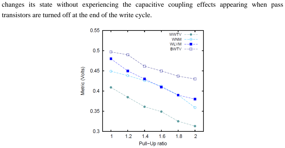
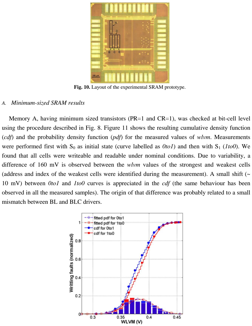
The central claim is that the write stability of a six-transistor SRAM bit cell can be quantified by a single externally observable number: the maximum word-line voltage drop that still lets the cell be overwritten. The paper shows that this number, WLVM, can be measured without touching the bit cell or the bit lines. The procedure writes the complementary state into a cell while the word-line voltage is stepped down by increments Δ, reads the cell back at nominal conditions after each attempt, and records the largest decrement for which the write still succeeds; the final WLVM for a cell is the minimum of the values obtained for the 0-to-1 and 1-to-0 write directions. In the minimum-sized 65 nm array these two directions differ, with a correlation of only r=0.2826, so both must be measured to identify weak cells. Across a 2048-cell array, WLVM spans roughly 160 mV between the strongest and weakest cell, and the mean value drops from 405 mV to 262 mV as the pull-up ratio rises from 1 to 2, rising to 482 mV for a pull-up ratio of 0.5, in agreement with simulation trends. The paper also reports that WLVM has a simulated linear correlation near 0.93 with both the bit-line write trip voltage and the word-line write trip voltage, while requiring none of the analogue switch arrays those metrics need.
Load-bearing premise
The search assumes that write success is monotone in word-line voltage: if a cell fails to write at one reduced voltage, it will also fail at every lower voltage, so stepping downward finds a clean single threshold without missing a narrow band of successful writes at lower voltages.
Editorial extensions
If this is right
- Every cell in a functional SRAM array can be assigned a per-cell WLVM, so cells that are hard to overwrite can be located by address instead of inferred from separate test structures.
- Because the measurement is only a write-and-read-back sequence with an adjustable word-line supply, it can be applied at bit, word, block, or full-memory level, trading resolution for test time.
- The simulated correlation near 0.93 with BWTV and WWTV indicates that WLVM ranks cells nearly the same way as established metrics while eliminating bit-line current monitoring and the associated switch arrays.
- WLVM distributions respond to pull-up ratio and transistor width in the expected direction, giving a quantitative, experimentally observable handle on how variability and sizing affect write-failure probability.
- The row-decoder modification is compatible with write-assist techniques, so the margin measurement can coexist with other word-line voltage adjustments already present in low-power memories.
Reading between the lines
- An extension the paper leaves implicit is using the same VDD_WL knob to probe read stability, since read-disturb margin also varies with word-line voltage; the identical read-back search could find the maximum word-line voltage that does not disturb stored data.
- The 0.93 correlation with BWTV and WWTV comes from simulation, not from simultaneous hardware measurement; putting all three metrics on the same die would test whether the ranking survives real process noise and measurement error.
- Because the procedure needs no special test mode beyond ordinary write and read operations, it could be embedded as a production or in-field self-test with an on-chip adjustable word-line supply, turning WLVM into a drift and variability sensor.
Editorial analysis
A structured set of objections, weighed in public.
Referee Report
Summary. The paper proposes Word-Line Voltage Margin (WLVM), defined as the maximum reduction of the word-line voltage that still allows an SRAM cell to be written, as an experimental writability metric. The measurement requires only a row-decoder modification providing a dedicated VDD_WL supply to the last decoder stage; the cell is written at progressively lower VDD_WL values and read back under nominal conditions. The authors validate the metric in Monte Carlo simulation against BWTV and WWTV, showing a linear correlation around 0.93, and then report measurements on a 65 nm CMOS prototype with five cell designs differing in pull-up ratio, demonstrating that the measured WLVM distributions exhibit the expected PR dependence and a spread attributable to process variability.
Significance. If the proposed technique is sound, it offers a practical, low-overhead way to obtain bit-level write-stability information from functional SRAM arrays without internal-node access, which would be valuable for weak-cell identification, yield analysis, and post-process characterization. The paper's main strength is the direct experimental demonstration: Table III and Fig. 14 show measured WLVM means within a few millivolts of simulation across five cell designs, and the monotonic dependence on pull-up ratio is consistent with device physics. The correlation with established writability metrics, however, is demonstrated only in simulation, not on the same test chip, and the search algorithm relies on an untested monotonicity assumption. The experimental data and the simple instrumentation are useful contributions, but the central measurement logic needs additional validation before the metric can be accepted as a reliable per-cell ranking tool.
major comments (4)
- [Section V-A, Table II] The search algorithm assumes that write success is monotonically non-decreasing with word-line voltage, but this is never established. The procedure records the first voltage step j at which a cell fails and then never revisits that cell; if a later attempt at a lower VDD_WL succeeds, due to probabilistic write behavior, bit-line coupling effects, or word-line pulse-shape changes, the stored wlvm value would be wrong and the ranked distributions in Figs. 11-14 would be distorted. Since the test chip already provides VDD_WL control and readback, this assumption should be checked directly by repeating the measurement on the same cells and by sweeping VDD_WL both downward and upward to test for hysteresis.
- [Section V-A, Table II] The textual description of the algorithm is internally inconsistent with the definition of WLVM. The paper defines WLVM as the maximum voltage reduction that still allows writing, but the algorithm updates wlvm_i to the first failing step (the minimum failing drop), not the last successful drop, and the sentence 'This procedure finishes when any cell can be written to the their complementary value' would terminate the loop at the first iteration if taken literally. The authors should rewrite the procedure to state clearly whether wlvm records the last success or the first failure, give the correct termination condition, and reconcile the notation 'min(jΔ)' with the physical quantity being reported.
- [Section V-A, Table II] The measurement step Δ is never specified for the experimental results, despite the fact that quantization effects are acknowledged for the simulations (Section IV, Fig. 6). Without knowing Δ, the reported means and standard deviations in Table II and Table III cannot be interpreted, and the resolution of the per-cell ranking is unknown. Please state the step size used in the prototype measurements and, if the step is not negligible relative to the observed standard deviations, discuss the resulting quantization error.
- [Section IV, Fig. 6] The claim of 'good correlation with existing writability metrics' is supported only by Monte Carlo simulation, not by experimental cross-measurement on the prototype. The abstract and introduction state this property without qualification, which overstates the evidence. Please qualify the claim in the abstract and conclusions, or provide experimental measurements of BWTV/WWTV on the same test chip for at least one cell type.
minor comments (4)
- [Section V-A, Table II] The text in Section V-A says the technique was applied at byte level, and Fig. 13 is described as byte-level results, but Table II labels the same level as 'Word level'. Please make the terminology consistent.
- [Abstract] There are minor language issues, including 'Their experimental measurement can be attained' in the abstract and the keyword 'SRAM estability' (should be 'stability'). A copyedit pass would be beneficial.
- [Section IV-B] The overline notation for the complementary state XS is not typeset clearly in the provided text; please use a distinct symbol (e.g., XS_bar or a different variable name) to avoid confusion between the two states.
- [Section IV, Fig. 5] The text states that WLVM was compared to WNM, BWTV, and WWTV in Fig. 5, but the correlation analysis in Fig. 6 only covers BWTV and WWTV. Please either add the WNM comparison to Fig. 6 or state explicitly that the WNM comparison is limited to the PR-trend plot.
Circularity Check
No significant circularity: WLVM is defined operationally and measured directly; the simulation correlations and PR-dependence experiments are independent checks, and the self-citations are implementation references rather than load-bearing arguments.
full rationale
The paper proposes WLVM as an operational quantity defined directly in Section IV as the maximum word-line voltage reduction that still allows a write, and Section IV-B measures it by an explicitly described decrement-and-readback search. No equation in the paper defines WLVM in terms of WWTV, BWTV, or WNM, nor are any of those metrics fitted to the WLVM data; the correlation in Fig. 6 is computed from independent Monte Carlo simulations using the same technology models, and the PR dependence in Table III is measured on a dedicated 65 nm prototype and compared with simulation, not forced by a fitted parameter. The authors cite their own prior work ([7], [9], [10], [19]) for the decoder modification, write-assist compatibility, area overhead, and regular-layout guidelines, but these are engineering implementation details and are not invoked as uniqueness theorems or as evidence that WLVM is equivalent to another metric. The untested monotonicity of write success versus word-line voltage in the Section IV-B search is a legitimate empirical correctness risk, but it is a measurement-assumption issue, not a circular reduction. The central claim remains self-contained: a direct experimental measurement plus an independent comparison with established writability metrics.
Assumptions & free parameters
free parameters (1)
- Measurement step size Δ (VDD_WL decrement) =
Not reported for silicon measurements; 10 mV used in simulation
assumptions (4)
- domain assumption The separatrix model of the 6T SRAM bistable latch correctly describes write operation dynamics (Section II, equations in [11]-[12]).
- domain assumption Write success is monotonically non-decreasing with word-line voltage (Section IV.B, Fig. 8 search algorithm).
- domain assumption Read operations at nominal conditions after each write attempt do not disturb the cell state, even for cells that nearly failed the write (Section IV.B).
- domain assumption The commercial 65 nm CMOS process design kit and Monte Carlo model accurately represent the silicon behavior of the fabricated prototype (Sections IV, V, Fig. 9/14).
Cite this review
Pith. "Pith review of An Affordable Experimental Technique for SRAM Write Margin Characterization for Nanometer CMOS Technologies." pith.science (2026). https://pith.science/paper/WJLN3RNE
@misc{pith2026241115521,
  author       = {Pith},
  title        = {Pith review of: An Affordable Experimental Technique for SRAM Write Margin Characterization for Nanometer CMOS Technologies},
  year         = {2026},
  howpublished = {\url{https://pith.science/paper/WJLN3RNE}},
  note         = {Machine review of arXiv:2411.15521}
}
read the original abstract
Increased process variability and reliability issues present a major challenge for future SRAM trends. Non-intrusive and accurate SRAM stability measurement is crucial for estimating yield in large SRAM arrays. Conventional SRAM variability metrics require including test structures that cannot be used to investigate cell bit fails in functional SRAM arrays. This work proposes the Word Line Voltage Margin (WLVM), defined as the maximum allowed word-line voltage drop during write operations, as a metric for the experimental characterization of write stability of SRAM cells. Their experimental measurement can be attained with minimal design modifications, while achieving good correlation with existing writability metrics. To demonstrate its feasibility, the distribution of WLVM values has been measured in an SRAM prototype implemented in 65 nm CMOS technology. The dependence of the metric with the width of the transistors has been also analysed, demonstrating their utility in post-process write stability characterization.
Figures


Figures from the paper (7 more)




Reference graph
Works this paper leans on
-
[1]
<http://www.itrs.net/> [October 2015]
International technology roadmap for semiconductors. <http://www.itrs.net/> [October 2015]
work page 2015
- [2]
-
[3]
J. Wang, S. Nalam , B.H. Calhoun, Analysing Static and Dynamic Write Margin for nanometers SRAMs, ACM/IEEE International Symposium on Low Power Electronics and Design (ISLPED) 2008, pp. 129-134
work page 2008
-
[4]
H. Aghababa, B. Ebrahimi, A. Afzali -Kusha, M. Pedram, Probability calculation of read failures in nano -scaled SRAM cells under process variations, Microelectron. Reliab. 52 (2012) 2805-2811
work page 2012
-
[5]
O. Hirabayashi, A. Kawasumi, A. Suzuki, Y. Takeyama, K. Kushiyama, T. Sasaki, A. Katayama, G. Fukano, Y. Fujimura, T. Nakazato, Y. Shizuki, N. Kushiyama, T. Yabe, A process-variation-tolerant dual power supply SRAM with 0.179 um 2 cell in 40nm CMOS using level -programmable wordl ine driver, IEEE International Solid -State Circuits Conference 2009, pp. 458-459
work page 2009
- [6]
-
[7]
C. Carmona, G. Torrens, B. Alorda, SRAM write margin cell estimation using wordline modulation and read/write operations, European Workshop on CMOS variability (VARI) 2014, pp 1-6
work page 2014
-
[8]
Z. Guo, A. Carlson, L. Pang, K. T. Duo ng, T. King Liu, B. Nikolic, Large-Scale SRAM Variability Characterization in 45nm CMOS, IEEE J. Solid-State Circuits 44 (2009) 3174-3192
work page 2009
Show all 19 references
-
[9]
Word-line power supply selector for stability improvement of embedded SRAMs in High Realiability Applications
B. Alorda C. Carmona, S. Bota. “Word-line power supply selector for stability improvement of embedded SRAMs in High Realiability Applications” Design Automation and Test in Europe Conference 2014, pp. 1-6
2014
-
[10]
Alorda, G
B. Alorda, G. Torrens, S. Bota, J. Segura, Adaptive static and dynamic noise margin improvement in minimum - sized 6T-SRAM cells, Microelectron. Reliab. 54 (2014) 2613-2620
2014
-
[11]
Analytical modeling of SRAM dynamic stability
B. Zhang, A. Arapostathis, S. Nassif, M. Orshansky, “Analytical modeling of SRAM dynamic stability” IEEE/ACM International Conference on Computer-Aided Design 2006, pp. 315–322
2006
-
[12]
Zhang,, P
Y. Zhang,, P. Li, G.M. Huang, Separatrices in high -dimensional state spa ce: system -theoretical tangent computation and application to SRAM dynamic stability analysis , 47th Design Automation Conference 2010, pp. 567-572
2010
-
[13]
Khalil, M
D. Khalil, M. Khellah, N. S. Kim, Y. Ismail, T. Karnik and V. K. De, Accurate Estimation of SRAM Dynamic Stability, IEEE Trans. Very Large Scale Integration (VLSI) Systems, 16 (2008) 1639-1647
2008
-
[14]
Design and Implementation of Dynamic Word - Line Pulse Write Margin Monitor for SRAM
Shao-Cheng Wang, Geng-Cing Lin, Yi-Wei Lin, Ming-Chien Tsai, Yi-Wei Chiu, Shyh-Jye Jou, Ching-Te Chuang, Nan-Chun Lien, Wei -Chiang Shih, Kuen-Di Lee, Jyun -Kai Chu, “Design and Implementation of Dynamic Word - Line Pulse Write Margin Monitor for SRAM” IEEE Asia Pacific Confer...
2012
-
[15]
Bhavnagarwala, S
A. Bhavnagarwala, S. Kosonocky, Yuen Chan, K. Stawiasz, U. Srinivasan, S. Kowalczyk, M. Ziegler, A sub-600 mV fluctuation tolerant 65nm CMOS SRAM array with dynamic cell biasing , IEEE J . Solid-State Circuits 43 (2008) 946-955
2008
-
[16]
Grossar , M
E. Grossar , M. Stucchi, K. Maex, W. Dehaene, Read stability and write -ability analysis of SRAM cells for nanometer technologies, IEEE J. Solid-State Circuits 41 (2006) 2577-2588
2006
-
[17]
Fisher, E
T. Fisher, E. Amirate, P. Huber, T. Nirschl, A. Olbrich, M. Ostermayr, D. Schmitt -Landsiedel, Analysis of read current and write trip voltage variability from a 1MB SRAM test structure , IEEE Trans. Semiconduct or Manufacture 21 (2008) 534-541
2008
-
[18]
A new combined methodology for write -margin extraction of advanced SRAM
N. Giercynski, B. Borot, N. Planes, H. Brut , “A new combined methodology for write -margin extraction of advanced SRAM”, IEEE International Conference on Microelectronic Test Structures 2007, pp. 97-100
2007
-
[19]
Torrens, S
G. Torrens, S. A. Bota, B. Alorda, J. Segura, An experimental approach to accurate alpha -SER modeling and optimization through design parameters in 6T SRAM cells for deep -nanometer CMOS, IEEE Trans.Device. Mater. Reliab. 14 (2014) 1013-1021
2014
Reviewed August 12, 2026 · model on record in the stance chip above.
Discussion (0). Continue with ORCID to comment.