REVIEW 3 major objections 3 minor 67 references
Disentangling morphology and conductance in amorphous graphene
T0 review · 3 major / 3 minor · reviewed 2026-08-12 · deepseek-v4-flash
Pith's one-line read The paper claims that the standard two-descriptor morphology space does not uniquely determine conductance in amorphous graphene, and that gate voltage can switch conduction between crystallite-based and defect-based hopping networks.
desk verdict A transparent, reproducible computational study whose central non-uniqueness claim hinges on an ad hoc site-radius cutoff that needs a sensitivity sweep. read the letter →
The pith
A machine-rendered reading of the paper's core claim, the machinery that carries it, and where it could break.
The reading
What carries the argument
The load-bearing object is the variable-range hopping network. Each thermally accessible tight-binding molecular orbital is converted into one or more hopping sites with a position and radius, using density-weighted k-means clustering; sites whose effective radius exceeds the largest crystalline inclusion in the ensemble are deleted as numerical artifacts. The hopping rate between sites $i$ and $j$ is written as $\omega_{ij} = \omega_0 e^{-\xi_{ij}}$, where $\xi_{ij}$ combines the site separation, the Gaussian overlap of the two site wavefunctions, and the site energies. Percolating a cluster that connects left and right edges of each 40 nm sample defines a critical $\xi_c$, and the ensemble conductance is the integral of $e^{-\xi}$ over the distribution of $\xi_c$. The second diagnostic object is the crystallinity $\chi$ of a site, the fraction of its electronic density lying on crystalline hexagons, which reveals where in the energy spectrum the conduction network lives.
What would settle it
Measure the conductance of a real AMC film whose ring statistics match sAMC-q400 (crystalline hexagons more abundant than isolated hexagons) rather than AMC-400: if it is insulating, the claimed non-uniqueness of the descriptor map would fail. Alternatively, recompute sAMC-q400 Fermi-energy conductance after varying the k-means localization thresholds (grid resolution, density cutoff, 20 \AA{} pocket separation, and the $a_{\max}$ cutoff) and check whether the $\approx 2.5\times 10^{-5}$ S prediction survives.
Extended reading notes
Core claim
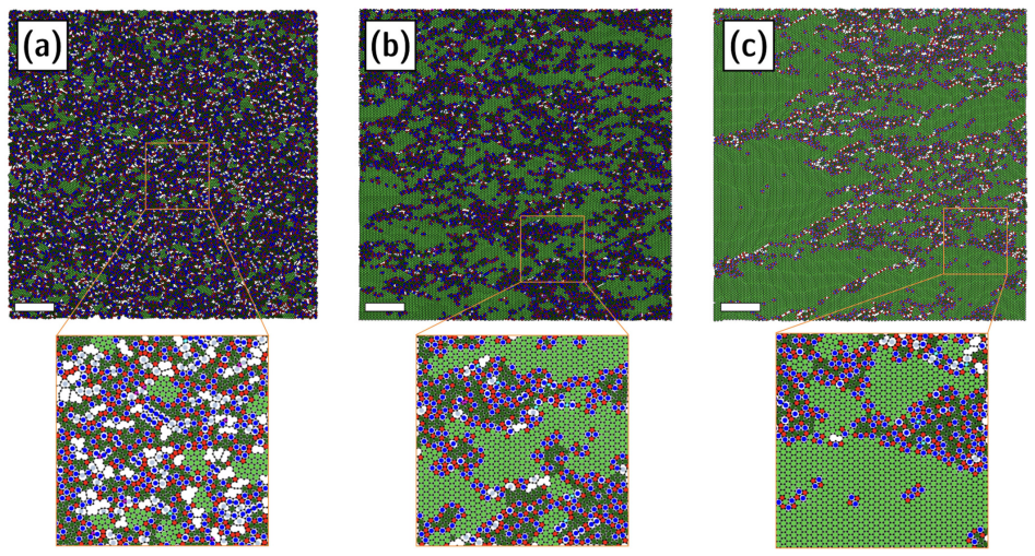
The paper's central discovery is that a unique map between $(\log \eta_{\mathrm{MRO}}, \rho_{\mathrm{sites}})$ and conductance does not exist for amorphous monolayer carbon. Its evidence is the sAMC-q400 ensemble: those structures occupy nearly the same descriptor coordinates as the experimentally insulating AMC-400, yet the percolation calculation puts their ungated conductance at $(2.51 \pm 0.40)\times 10^{-5}$ S, comparable to the ordered sAMC-300 ensemble. A second claim is that conduction networks are not controlled by atomic structure alone: variable-range hopping sites near the band edges sit preferentially on crystalline inclusions, while sites near the Fermi energy sit preferentially on defects. Because a gate voltage shifts the chemical potential through these regimes, the morphology of the conducting network can be changed while leaving the film itself unchanged.
Load-bearing premise
The results stand on the assumption that the protocol for turning delocalized tight-binding orbitals into hopping sites, namely k-means partitioning into high-density pockets followed by deletion of sites larger than the largest crystalline inclusion, does not systematically bias which morphologies receive sites or how those sites conduct.
Editorial extensions
If this is right
- The five-order-of-magnitude conductance gap between sAMC-300 and sAMC-500 reproduces the experimental gap, indicating that the percolation-based variable-range hopping model captures the dominant transport physics in these films.
- Because the same $(\log \eta_{\mathrm{MRO}}, \rho_{\mathrm{sites}})$ point can host both insulating and conducting samples, experimental classification of AMCs should include ring statistics and crystallite-size distributions, not just the two standard order parameters.
- Gate voltage can modulate conductance by selecting band-edge crystalline hopping networks or Fermi-energy defect networks, without any change to the atomic structure.
- The Fermi-energy preference for defects implies that ungated conductance is controlled by the defect network's density and connectivity, so defect engineering should be as effective as global crystallinity in designing conductive AMCs.
- The combination of gate-tunable electronic transport with low thermal conductance positions AMCs as potential thermoelectric materials, once their absolute conductivities are raised toward useful levels.
Reading between the lines
- A natural extension is that any low-dimensional morphology descriptor space will underdetermine transport in disordered two-dimensional carbons; descriptors that capture defect clustering rather than total defect fraction may restore a useful, though possibly multi-valued, structure-property relation.
- If defect-localized Fermi-energy states really carry the current, then deliberate defect patterning by irradiation, strain, or growth conditions could route current along engineered paths, a possibility the paper does not test.
- The predicted crystallite-to-defect crossover could be tested directly by spectrally resolved local density-of-state measurements at different gate voltages; if the crossover is absent, the k-means site construction is the likely culprit.
- The protocol's $a_{\max}$ cutoff is set by the largest crystalline inclusion in each ensemble, so the model implicitly assumes real localization radii never exceed that scale; samples with very large ordered domains might violate that assumption and shift the Fermi-energy conductance.
Editorial analysis
A structured set of objections, weighed in public.
Referee Report
Summary. This paper combines MAP-generated mesoscale amorphous graphene structures (sAMC-500, sAMC-q400, sAMC-300) with a tight-binding Lanczos partial diagonalization and a Miller-Abrahams variable-range hopping percolation model to compute ensemble conductances. The authors reproduce the experimentally reported five-order-of-magnitude conductance gap between the most and least ordered ensembles, predict that the sAMC-q400 ensemble conducts similarly to sAMC-300 despite lying near the insulating experimental AMC-400 in the (log η_MRO, ρ_sites) descriptor space, and conclude that a unique morphology-to-conductance map does not exist in this descriptor space. They also analyze the crystallinity of the hopping sites and report a metamorphosis from crystallite-localized conduction at band edges to defect-localized conduction near the Fermi energy.
Significance. The paper is methodologically transparent and has several genuine strengths: it provides a machine-precision benchmark of the Lanczos diagonalization against exact diagonalization (SI Section S6), makes code and data publicly available (SI Section S10), uses mesoscale aperiodic samples without periodic boundary conditions, and reproduces a nontrivial experimental conductance gap. If the central predictions are robust, the conclusion that partial morphology descriptors such as (log η_MRO, ρ_sites) cannot uniquely determine conductance would be a useful cautionary result for the amorphous-materials community, and the crystallinity analysis of conduction networks would open a genuinely new way to think about gate-controlled transport in AMCs. The strength of these claims, however, rests on the site-construction protocol in the VRH model, which is the main fragility discussed below.
major comments (3)
- [Supporting Information §S7; Table 1] The site-radius cutoff amax is an ensemble-dependent numerical filter that is load-bearing for the central conductance predictions. In the hopping-rate expression (Eq. S5) and overlap function f (Eq. S6), larger site radii increase inter-site overlap and therefore increase hopping rates; removing all sites with radius above the largest crystalline inclusion in each ensemble (Table 1: 18.03 Å for sAMC-500 versus 136.47 Å for sAMC-q400 and 199.33 Å for sAMC-300) disproportionately suppresses hopping in the most disordered ensemble while preserving very large sites in the ordered ones. The stated justification, that a physical site cannot be larger than the largest crystallite, is not established: VRH localization lengths are not bounded by crystallite size. Because the predicted sAMC-q400 conductance (G(μ=ε_F) = (2.51 ± 0.40)×10^-5 S, Table 1) and the resulting claim that no unique (log η_MRO, ρ_sites)-to-conductance map exists depend on this filter, I request a controlled sweep over amax or a physically derived localization-size criterion to show that the q400/sAMC-300 conductance overlap and the sAMC-500/sAMC-300 gap are not artifacts of the cutoff.
- [Supporting Information §S7; main text, 'Constructing the VRH network'] The k-means site-construction protocol is another load-bearing choice that is not validated. The manuscript classifies multi-pocket delocalized MOs as 'pathological' and partitions them into sites using a 100×100 grid, a density threshold of 0.3 of the maximum, and a minimum separation of 20 Å; these parameters are hand-selected, and the protocol is assumed not to bias the relative site density between crystalline and defective regions or between ensembles. Since the near-ε_F states are reported to be the most affected (main text), and since Figure 3d's 'conducting sites preferentially on defects' conclusion is based on these sites, the absence of any sensitivity analysis with respect to the clustering parameters or an alternative site-definition leaves open the possibility that the defect-localization and q400 conductance results are artifacts of the localization procedure.
- [Results, 'sAMC-q400' paragraph; Figure 2c] The non-uniqueness claim is stronger than the evidence presented. The sAMC-q400 ensemble is compared with the experimental AMC-400, but the two differ not only in the (log η_MRO, ρ_sites) position (which is close, not identical) but also in ring statistics: the manuscript states that the 6-c/6-i ratio is reversed relative to experiment (Figure 2c and main text). Because the experimental AMC-400 was not generated with the same MAP protocol and its conductance was measured in a different setup, the comparison conflates structural differences not captured by the two chosen descriptors with a genuine breakdown of the morphology-conductance map. The conclusion should be rephrased as showing that the two descriptors are insufficient, or supported by a simulated ensemble with experimentally matched ring statistics and a controlled comparison within the same simulation pipeline.
minor comments (3)
- [Throughout] The manuscript contains several typographical errors, including 'postitve' (p. 9), 'experimetnal' (SI Section S3), 'aloogrithm' (SI Section S5), 'devation' (SI Section S6), and 'pecularities' (p. 17).
- [Equation (S5); Table 1] The choice of the attempt frequency ω0 = 1 fs^-1 and the 4kBT energy window should be justified or tested; the absolute conductances in Table 1 scale with ω0, even if the relative gap does not.
- [Figure 3a and Table 1] Figure 3a states that error bars are omitted because they are too small to be visible, but Table 1 reports relative uncertainties of roughly 40–100% for several band-edge conductances (e.g., G(μ=ε0) for sAMC-500 = (2.99 ± 2.43)×10^-13 S); please clarify how these are represented in the figure.
Circularity Check
No circularity: conductance is a forward VRH/percolation model benchmarked against external data; the a_max filter is a robustness concern, not a fitted input.
full rationale
The paper's derivation chain is self-contained as a forward model. Tight-binding parameters are taken from prior external literature, the Miller-Abrahams form and percolation integral are standard, and no parameter is fitted to the experimental conductance values used for benchmarking. The reproduction of the five-order-of-magnitude conductance gap between sAMC-500 and sAMC-300 is an emergent prediction rather than a fit, and the claimed non-uniqueness of the (log-eta_MRO, rho_sites) map follows from comparing a separately generated sAMC-q400 ensemble against the experimental AMC-400 without using AMC-400's conductance as an input. The closest candidate to circularity is the ensemble-dependent a_max site-radius cutoff, which is heuristic and could bias relative conductances; however, the cutoff is set by a morphological quantity (largest crystalline inclusion), not by the target conductance, and the final conductance emerges from percolation over the resulting site network. A controlled a_max sweep would strengthen robustness, but this is a correctness/robustness risk rather than a circular reduction. Self-citations (MAP and prior nanojunction work) provide methodology and context; the central results are computed from published code and are anchored to external experimental benchmarks, so they do not constitute load-bearing self-citation circularity.
Assumptions & free parameters
free parameters (4)
- amax site-radius cutoff =
sAMC-500: 18.03 Å; sAMC-q400: 136.47 Å; sAMC-300: 199.33 Å
- k-means localization parameters =
grid 100x100; density threshold 0.3*max; minimum separation 20 Å; |φ|^4 weighting
- thermal energy window =
4k_BT ≈ 0.103 eV at T=300 K
- escape frequency ω0 =
1 fs^-1
assumptions (5)
- domain assumption The variable-range hopping picture with Miller-Abrahams hopping rates is the correct transport mechanism for these AMC films.
- domain assumption A nearest-neighbor tight-binding Hamiltonian with parameters from prior literature, restricted to π-electrons, adequately represents the electronic structure.
- ad hoc to paper Molecular orbitals with several disjoint high-density pockets are numerical artifacts to be artificially localized.
- domain assumption Percolation across the left and right edges of a 40 nm x 40 nm sample gives the ensemble conductance.
- standard math Gershgorin's theorem and the LDLT factorization correctly estimate the HOMO position.
Cite this review
Pith. "Pith review of Disentangling morphology and conductance in amorphous graphene." pith.science (2026). https://pith.science/paper/RENYHT7R
@misc{pith2026241118041,
  author       = {Pith},
  title        = {Pith review of: Disentangling morphology and conductance in amorphous graphene},
  year         = {2026},
  howpublished = {\url{https://pith.science/paper/RENYHT7R}},
  note         = {Machine review of arXiv:2411.18041}
}
read the original abstract
Amorphous graphene or amorphous monolayer carbon (AMC) is a family of carbon films that exhibit a surprising sensitivity of electronic conductance to morphology. We combine deep learning-enhanced simulation techniques with percolation theory to analyze three morphologically distinct mesoscale AMCs. Our approach avoids the pitfalls of applying periodic boundary conditions to these fundamentally aperiodic systems or equating crystalline inclusions with conducting sites. We reproduce the previously reported dependence of charge conductance on morphology and explore the limitations of partial morphology descriptors in witnessing conductance properties. Finally, we perform crystallinity analysis of conductance networks along the electronic energy spectrum and show that they metamorphose from being localized on crystallites at band edges to localized on defects around the Fermi energy opening the possibility of control through gate voltage.
Figures


Reference graph
Works this paper leans on
-
[2]
Toh, C.-T.; Zhang, H.; Lin, J.; Mayorov, A. S.; Wang, Y.-P.; Orofeo, C. M.; Ferry, D. B.; Andersen, H.; Kakenov, N.; Guo, Z. et al. Synthesis and properties of free-standing monolayer amorphous carbon. Nature 2020, 577, 199--203
work page 2020
-
[3]
Electronic structure of a realistic model of amorphous graphene
Kapko, V.; Drabold, D.; Thorpe, M. Electronic structure of a realistic model of amorphous graphene. physica status solidi (b) 2010, 247, 1197--1200
work page 2010
-
[4]
Insulating behavior of an amorphous graphene membrane
Van Tuan, D.; Kumar, A.; Roche, S.; Ortmann, F.; Thorpe, M.; Ordejon, P. Insulating behavior of an amorphous graphene membrane. Physical Review B 2012, 86, 121408
work page 2012
-
[5]
A.; Niquet, Y.-M.; Delcorte, A.; Charlier, J.-C
Lherbier, A.; Roche, S.; Restrepo, O. A.; Niquet, Y.-M.; Delcorte, A.; Charlier, J.-C. Highly defective graphene: A key prototype of two-dimensional Anderson insulators. Nano Research 2013, 6, 326--334
work page 2013
-
[6]
Phonons, localization, and thermal conductivity of diamond nanothreads and amorphous graphene
Zhu, T.; Ertekin, E. Phonons, localization, and thermal conductivity of diamond nanothreads and amorphous graphene. Nano letters 2016, 16, 4763--4772
work page 2016
-
[7]
Thermal transport in amorphous graphene with varying structural quality
Antidormi, A.; Colombo, L.; Roche, S. Thermal transport in amorphous graphene with varying structural quality. 2D Materials 2020, 8, 015028
work page 2020
-
[8]
Amorphous graphene: a realization of Zachariasen’s glass
Kumar, A.; Wilson, M.; Thorpe, M. Amorphous graphene: a realization of Zachariasen’s glass. Journal of Physics: Condensed Matter 2012, 24, 485003
work page 2012
-
[9]
Zhang, Y.-T.; Wang, Y.-P.; Zhang, X.; Zhang, Y.-Y.; Du, S.; Pantelides, S. T. Structure of amorphous two-dimensional materials: elemental monolayer amorphous carbon versus binary monolayer amorphous boron nitride. Nano Letters 2022, 22, 8018--8024
work page 2022
Show all 67 references
-
[10]
Stone--wales defects preserve hyperuniformity in amorphous two-dimensional networks
Chen, D.; Zheng, Y.; Liu, L.; Zhang, G.; Chen, M.; Jiao, Y.; Zhuang, H. Stone--wales defects preserve hyperuniformity in amorphous two-dimensional networks. Proceedings of the National Academy of Sciences 2021, 118, e2016862118
2021
-
[11]
C.; Tromer, R
Felix, L. C.; Tromer, R. M.; Autreto, P. A.; Ribeiro Junior, L. A.; Galvao, D. S. On the mechanical properties and thermal stability of a recently synthesized monolayer amorphous carbon. The Journal of Physical Chemistry C 2020, 124, 14855--14860
2020
-
[12]
Tian, H.; Ma, Y.; Li, Z.; Cheng, M.; Ning, S.; Han, E.; Xu, M.; Zhang, P.-F.; Zhao, K.; Li, R. et al. Disorder-tuned conductivity in amorphous monolayer carbon. Nature 2023, 615, 56--61
2023
-
[13]
Y.; Bengio, Y.; Simine, L
Kilgour, M.; Gastellu, N.; Hui, D. Y.; Bengio, Y.; Simine, L. Generating multiscale amorphous molecular structures using deep learning: a study in 2D. The Journal of Physical Chemistry Letters 2020, 11, 8532--8537
2020
-
[14]
D.; Simine, L
Madanchi, A.; Kilgour, M.; Zysk, F.; K \"u hne, T. D.; Simine, L. Simulations of disordered matter in 3D with the morphological autoregressive protocol (MAP) and convolutional neural networks. The Journal of Chemical Physics 2024, 160, 024101
2024
-
[15]
L.; Cs \'a nyi, G
Deringer, V. L.; Cs \'a nyi, G. Machine learning based interatomic potential for amorphous carbon. Physical Review B 2017, 95, 094203
2017
-
[16]
Anderson, P. W. Absence of diffusion in certain random lattices. Physical review 1958, 109, 1492
1958
-
[17]
Thouless, D. J. Electrons in disordered systems and the theory of localization. Physics Reports 1974, 13, 93--142
1974
-
[18]
A.; Ramakrishnan, T
Lee, P. A.; Ramakrishnan, T. V. Disordered electronic systems. Reviews of modern physics 1985, 57, 287
1985
-
[19]
F.; Davis, E
Mott, N. F.; Davis, E. A. Electronic processes in non-crystalline materials; Oxford University Press Oxford, 1971; Vol. 14
1971
-
[20]
Hopping conductivity in disordered systems
Ambegaokar, V.; Halperin, B.; Langer, J. Hopping conductivity in disordered systems. Physical review B 1971, 4, 2612
1971
-
[21]
I.; Efros, A
Shklovskii, B. I.; Efros, A. L. Electronic properties of doped semiconductors; Springer Science & Business Media, 1984; Vol. 45
1984
-
[22]
Sterpone, F.; Rossky, P. J. Molecular modeling and simulation of conjugated polymer oligomers: Ground and excited state chain dynamics of PPV in the gas phase. The Journal of Physical Chemistry B 2008, 112, 4983--4993
2008
-
[23]
E.; Willard, A
Jailaubekov, A. E.; Willard, A. P.; Tritsch, J. R.; Chan, W.-L.; Sai, N.; Gearba, R.; Kaake, L. G.; Williams, K. J.; Leung, K.; Rossky, P. J. et al. Hot charge-transfer excitons set the time limit for charge separation at donor/acceptor interfaces in organic photovoltaics. Nat...
2013
-
[24]
H.; Van Loan, C
Golub, G. H.; Van Loan, C. F. Matrix Computations, 3rd ed.; JHU press, 1996; pp 470--499
1996
-
[25]
C.; Geim, A
Meyer, J. C.; Geim, A. K.; Katsnelson, M. I.; Novoselov, K. S.; Booth, T. J.; Roth, S. The structure of suspended graphene sheets. Nature 2007, 446, 60--63
2007
-
[26]
Stone-Wales defects in graphene and other planar sp 2-bonded materials
Ma, J.; Alf \`e , D.; Michaelides, A.; Wang, E. Stone-Wales defects in graphene and other planar sp 2-bonded materials. Physical Review B—Condensed Matter and Materials Physics 2009, 80, 033407
2009
-
[27]
Electrical resistivity of polycrystalline graphene: Effect of grain-boundary-induced strain fields
Krasavin, S.; Osipov, V. Electrical resistivity of polycrystalline graphene: Effect of grain-boundary-induced strain fields. Scientific Reports 2022, 12, 14553
2022
-
[28]
Impurity band and conductivity of compensated semiconductors
Shklovskii, B.; Efros, A. Impurity band and conductivity of compensated semiconductors. Soviet physics JETP 1971, 33, 468--474
1971
-
[29]
Percolation and conductivity: A computer study
Pike, G.; Seager, C. Percolation and conductivity: A computer study. I. Physical review B 1974, 10, 1421
1974
-
[30]
A hopping model for activated charge transport in amorphous silicon
Gr \"u newald, M.; Thomas, P. A hopping model for activated charge transport in amorphous silicon. physica status solidi (b) 1979, 94, 125--133
1979
-
[31]
Theory of the field-effect mobility in amorphous organic transistors
Vissenberg, M.; Matters, M. Theory of the field-effect mobility in amorphous organic transistors. Physical Review B 1998, 57, 12964
1998
-
[32]
Percolation approach to hopping transport in organic disordered solids
Baranovskii, S.; Zvyagin, I.; Cordes, H.; Yamasaki, S.; Thomas, P. Percolation approach to hopping transport in organic disordered solids. physica status solidi (b) 2002, 230, 281--288
2002
-
[33]
Concentration dependence of the hopping mobility in disordered organic solids
Rubel, O.; Baranovskii, S.; Thomas, P.; Yamasaki, S. Concentration dependence of the hopping mobility in disordered organic solids. Physical Review B 2004, 69, 014206
2004
-
[34]
A percolation approach to the temperature and charge carrier concentration dependence of the hopping conductivity in organic materials
Zvyagin, I. A percolation approach to the temperature and charge carrier concentration dependence of the hopping conductivity in organic materials. physica status solidi c 2008, 5, 725--729
2008
-
[35]
Hopping transport in systems of finite thickness or length
Rodin, A.; Fogler, M. Hopping transport in systems of finite thickness or length. Physical Review B 2011, 84, 125447
2011
-
[36]
Advanced percolation solution for hopping conductivity
Nenashev, A.; Jansson, F.; Oelerich, J.; Huemmer, D.; Dvurechenskii, A.; Gebhard, F.; Baranovskii, S. Advanced percolation solution for hopping conductivity. Physical Review B 2013, 87, 235204
2013
-
[37]
Molecular geometry fluctuations and field-dependent mobility in conjugated polymers
Yu, Z.; Smith, D.; Saxena, A.; Martin, R.; Bishop, A. Molecular geometry fluctuations and field-dependent mobility in conjugated polymers. Physical Review B 2001, 63, 085202
2001
-
[38]
Scaling of current distributions in variable-range hopping transport on two-and three-dimensional lattices
Pasveer, W.; Bobbert, P.; Huinink, H.; Michels, M. Scaling of current distributions in variable-range hopping transport on two-and three-dimensional lattices. Physical Review B 2005, 72, 174204
2005
-
[39]
Charge transport in disordered organic photoconductors
B \"a ssler, H. Charge transport in disordered organic photoconductors. A Monte Carlo simulation study. Physica Status Solidi B (Basic Research);(Germany) 1993, 175, 15--56
1993
-
[40]
T.; Liu, W.; Balzer, D.; Kassal, I
Willson, J. T.; Liu, W.; Balzer, D.; Kassal, I. Jumping kinetic Monte Carlo: Fast and accurate simulations of partially delocalized charge transport in organic semiconductors. The Journal of Physical Chemistry Letters 2023, 14, 3757--3764
2023
-
[41]
Private electronic correspondence, 2024-04-26
Liu, L. Private electronic correspondence, 2024-04-26
2024
-
[42]
Electronic conduction through monolayer amorphous carbon nanojunctions
Gastellu, N.; Kilgour, M.; Simine, L. Electronic conduction through monolayer amorphous carbon nanojunctions. The Journal of Physical Chemistry Letters 2022, 13, 339--344
2022
-
[43]
Zachariasen, W. H. The atomic arrangement in glass. Journal of the American Chemical Society 1932, 54, 3841--3851
1932
-
[44]
Atomistic structure of band-tail states in amorphous silicon
Dong, J.; Drabold, D. Atomistic structure of band-tail states in amorphous silicon. Physical review letters 1998, 80, 1928
1998
-
[45]
Universal features of localized eigenstates in disordered systems
Ludlam, J.; Taraskin, S.; Elliott, S.; Drabold, D. Universal features of localized eigenstates in disordered systems. Journal of Physics: Condensed Matter 2005, 17, L321
2005
-
[46]
F.; Davis, E
Mott, N. F.; Davis, E. A. Electronic processes in non-crystalline materials; OUP Oxford, 2012
2012
-
[47]
I.; Barker, A
Liu, J.; van der Zee, B.; Alessandri, R.; Sami, S.; Dong, J.; Nugraha, M. I.; Barker, A. J.; Rousseva, S.; Qiu, L.; Qiu, X. et al. N-type organic thermoelectrics: demonstration of ZT> 0.3. Nature communications 2020, 11, 5694
2020
-
[48]
Zhao, J.; Zhu, G.; Huang, W.; He, Z.; Feng, X.; Ma, Y.; Dong, X.; Fan, Q.; Wang, L.; Hu, Z. et al. Synthesis of large-scale undoped and nitrogen-doped amorphous graphene on MgO substrate by chemical vapor deposition. Journal of Materials Chemistry 2012, 22, 19679--19683 mcitet...
2012 arXiv
-
[49]
Conditional image generation with pixelcnn decoders
Van den Oord, A.; Kalchbrenner, N.; Espeholt, L.; Vinyals, O.; Graves, A., et al. Conditional image generation with pixelcnn decoders. Advances in neural information processing systems 2016, 29
2016
-
[50]
Pixel recurrent neural networks
Van Den Oord, A.; Kalchbrenner, N.; Kavukcuoglu, K. Pixel recurrent neural networks. International conference on machine learning. 2016; pp 1747--1756
2016
-
[51]
sAMC generation
Madanchi , A.; Gastellu , N. sAMC generation . sAMC\_generation v1.0.1 on Zenodo , https://doi.org/10.5281/zenodo.15085683
-
[52]
El-Machachi, Z.; Wilson, M.; Deringer, V. L. Exploring the configurational space of amorphous graphene with machine-learned atomic energies. Chemical Science 2022, 13, 13720--13731
2022
-
[53]
J.; Tutein, A
Stuart, S. J.; Tutein, A. B.; Harrison, J. A. A reactive potential for hydrocarbons with intermolecular interactions. The Journal of chemical physics 2000, 112, 6472--6486
2000
-
[54]
Fast parallel algorithms for short-range molecular dynamics
Plimpton, S. Fast parallel algorithms for short-range molecular dynamics. Journal of computational physics 1995, 117, 1--19
1995
-
[55]
P.; Aktulga, H
Thompson, A. P.; Aktulga, H. M.; Berger, R.; Bolintineanu, D. S.; Brown, W. M.; Crozier, P. S.; In't Veld, P. J.; Kohlmeyer, A.; Moore, S. G.; Nguyen, T. D., et al. LAMMPS-a flexible simulation tool for particle-based materials modeling at the atomic, meso, and continuum scale...
2022
-
[56]
Disorder-tuned conductivity in amorphous monolayer carbon
Tian, H.; Ma, Y.; Li, Z.; Cheng, M.; Ning, S.; Han, E.; Xu, M.; Zhang, P.-F.; Zhao, K.; Li, R., et al. Disorder-tuned conductivity in amorphous monolayer carbon. Nature 2023, 615, 56--61
2023
-
[57]
Defects, tight binding, and first-principles molecular-dynamics simulations on a-Si
Fedders, P.; Drabold, D.; Klemm, S. Defects, tight binding, and first-principles molecular-dynamics simulations on a-Si. Physical Review B 1992, 45, 4048
1992
-
[58]
Consistency requirement in the Pariser-Parr-Pople model
Linderberg, J. Consistency requirement in the Pariser-Parr-Pople model. Chemical Physics Letters 1967, 1, 39--41
1967
-
[59]
E.; Willard, A
Jailaubekov, A. E.; Willard, A. P.; Tritsch, J. R.; Chan, W.-L.; Sai, N.; Gearba, R.; Kaake, L. G.; Williams, K. J.; Leung, K.; Rossky, P. J., et al. Hot charge-transfer excitons set the time limit for charge separation at donor/acceptor interfaces in organic photovoltaics. Na...
2013
-
[60]
The spectral transformation Lanczos method for the numerical solution of large sparse generalized symmetric eigenvalue problems
Ericsson, T.; Ruhe, A. The spectral transformation Lanczos method for the numerical solution of large sparse generalized symmetric eigenvalue problems. Mathematics of Computation 1980, 35, 1251--1268
1980
-
[61]
Higham, N. J. Functions of matrices: theory and computation; SIAM, 2008; p 323
2008
-
[62]
Least squares quantization in PCM
Lloyd, S. Least squares quantization in PCM. IEEE transactions on information theory 1982, 28, 129--137
1982
-
[63]
Pedregosa, F. et al. Scikit-learn: Machine Learning in P ython. Journal of Machine Learning Research 2011, 12, 2825--2830
2011
-
[64]
Impurity conduction at low concentrations
Miller, A.; Abrahams, E. Impurity conduction at low concentrations. Physical Review 1960, 120, 745
1960
-
[65]
Economou, E.; Cohen, M. H. Localization in disordered materials: Existence of mobility edges. Physical Review Letters 1970, 25, 1445
1970
-
[66]
ArpackMAC
Gastellu , N. ArpackMAC . ArpackMAC v1.0.0.01 on Zenodo , https://doi.org/10.5281/zenodo.15131343
-
[67]
PercolateMAC
Gastellu , N. PercolateMAC . percolate\_mac v1.0.0 on Zenodo , https://doi.org/10.5281/zenodo.15078860
-
[68]
) retain a highly crystalline character, while their near- _F MOs are concentrated near ``defects
Gastellu , N. DisorderAnalysisMAC . disorder\_analysis\_MAC v1.0.0 on Zenodo , https://doi.org/10.5281/zenodo.15081260 mcitethebibliography supp_info.tex0000664000000000000000000012410714776127052012322 0ustar rootroot [journal=jacsat,manuscript=article] achemso chemformula [T...
Reviewed August 12, 2026 · model on record in the stance chip above.
Discussion (0). Continue with ORCID to comment.