REVIEW 3 major objections 4 minor 1 cited by
All-electrical near-field injection of excitons in a van der Waals antiferromagnet
T0 review · 3 major / 4 minor · reviewed 2026-08-07 · deepseek-v4-flash
Pith's one-line read Tunneling electrons electrically excite excitons in CrSBr from cryogenic to room temperature.
desk verdict Solid first demonstration of all-electrical exciton injection in CrSBr; the polariton identification is suggestive but underconstrained. read the letter →
The pith
A machine-rendered reading of the paper's core claim, the machinery that carries it, and where it could break.
The reading
What carries the argument
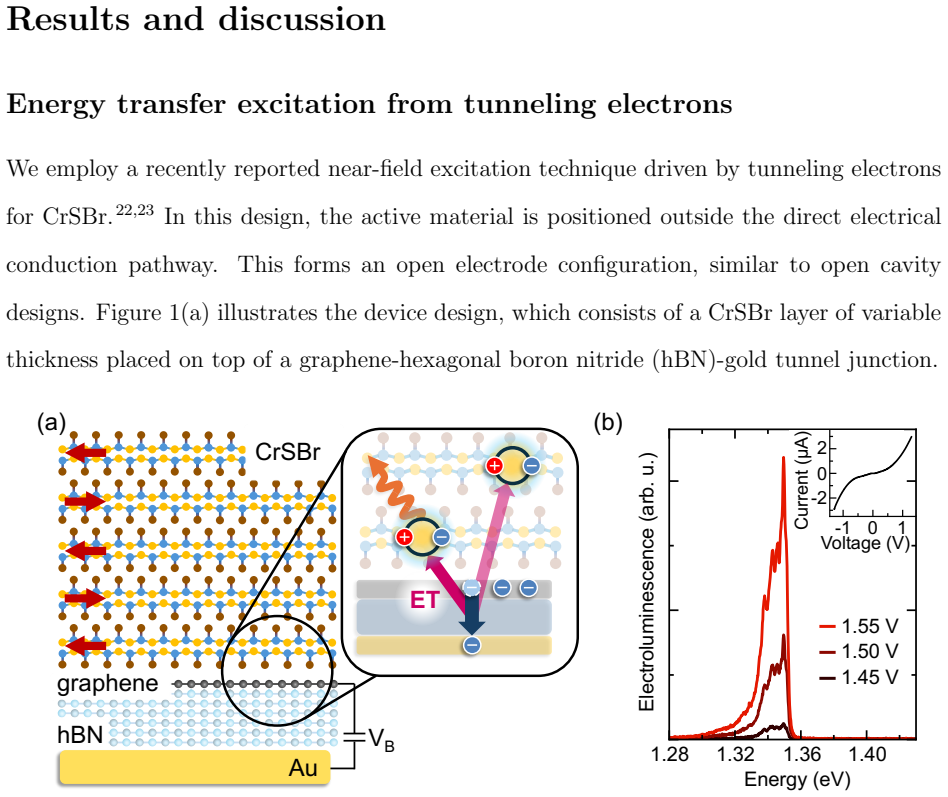
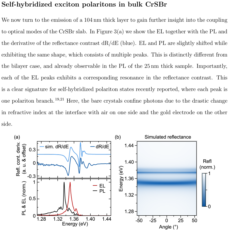
The key mechanism is the open-electrode tunnel junction: a graphene electrode, a few-layer hBN tunneling barrier, and a gold electrode, with the CrSBr placed on top so that it is not part of the conduction path. Inelastic tunneling electrons lose energy to the nearby exciton via near-field energy transfer, exciting charge-neutral excitons in the proximate CrSBr layers, with the coupling strength set by the exciton oscillator strength, the dipole orientation, and the separation between the junction and the flake. For thick flakes, the relevant final states are self-hybridized exciton polaritons, modes formed when the CrSBr slab itself confines photons because of the refractive-index contrast at its interfaces, and the paper models these with a transfer-matrix calculation using a single exciton resonance to reproduce the measured reflectance and electroluminescence peaks.
What would settle it
Measure electroluminescence from an identical graphene–hBN–gold tunnel junction with no CrSBr on top under the same bias: the excitonic line near 1.35 eV and its b-axis linear polarization should disappear, leaving only broadband emission; if they persist, the excitonic origin of the signal would be disproved.
Extended reading notes
Core claim
The central claim is that strongly bound excitons in CrSBr can be excited purely electrically by near-field energy transfer from inelastic tunneling electrons, without applying a bias across the CrSBr itself. The evidence is spectrally sharp electroluminescence at roughly 1.35 eV that tracks the exciton resonances seen in photoluminescence, together with strong linear polarization along the b-axis, which rules out ordinary broadband hot-electron emission as the dominant process. In bilayer samples the emission is attributed to the magnetically confined surface exciton, while in thick flakes up to 250 nm the multiple electroluminescence peaks coincide with the reflectance resonances of self-hybridized exciton polaritons, so the authors conclude that the electrical excitation populates polariton branches. The same mechanism is reported to work from 5 K up to room temperature, with the excitonic emission weakening as magnetic order is lost near the Néel temperature.
Load-bearing premise
The polariton assignment for thick flakes depends on the transfer-matrix model's dielectric function, which is estimated from a single exciton resonance at 1.387 eV taken from prior work; if that dielectric response is inaccurate, the match between electroluminescence peaks and reflectance resonances could be coincidental.
Editorial extensions
If this is right
- Electrically driven exciton emission can be obtained in CrSBr without passing current through the magnetic material itself, avoiding charge-injection damage and charge imbalance.
- The same device geometry works across a large thickness range, from a bilayer to 250 nm, so the excitation does not depend on the active layer being thin or electrically conductive.
- Thick CrSBr flakes act as electrically driven sources of self-hybridized exciton polaritons, coupling excitonic emission to confined optical modes.
- Emission persists up to room temperature, although the excitonic contribution weakens as magnetic order disappears near the Néel temperature.
- The linear polarization of the electroluminescence along the b-axis provides an all-electrical route to sense the crystal and magnetic axes of the material.
Reading between the lines
- The same near-field injection scheme should in principle work for other van der Waals semiconductors and magnets with strong exciton oscillator strengths, not only CrSBr, provided the excitons lie close enough to the tunnel junction.
- Because only the layers nearest the junction are excited, this technique could serve as an interface-sensitive probe of exciton properties, complementing bulk photoluminescence measurements.
- If the graphene Fermi level is tuned to reduce quenching, the external quantum efficiency, which the authors report as a lower bound, might be substantially improved.
- The expected excitation of hyperbolic exciton polaritons and graphene-gold surface plasmons suggests that voltage could be used to switch between different radiative channels in the same device.
Editorial analysis
A structured set of objections, weighed in public.
Referee Report
Summary. The manuscript reports a device geometry in which a graphene/hBN/gold tunnel junction is placed underneath a CrSBr flake, and inelastic electron tunneling excites excitons in the CrSBr via near-field energy transfer without direct charge injection into the semiconductor. Electroluminescence is observed from flakes of nominal thickness from bilayer to 104 nm (claimed up to 250 nm) and at temperatures from 5 K up to, the authors claim, room temperature. The emission is linearly polarized along the crystallographic b-axis, largely overlaps spectrally with photoluminescence, and shifts near the Néel temperature, supporting an excitonic origin. For a 104 nm flake, the emission spectrum exhibits multiple peaks that the authors attribute to self-hybridized exciton polaritons, based on matching to reflectance-contrast features computed with a transfer-matrix model using a single-exciton resonance. The paper also presents voltage-dependent external quantum efficiency, local-density-of-states calculations, and a discussion of the excitation mechanism.
Significance. If the central observation holds, this is a valuable first demonstration of electrically driven excitonic emission in a van der Waals magnet, with a device scheme that avoids direct charge injection and that operates across a range of flake thicknesses. The core result—electrically excited, linearly polarized exciton emission from CrSBr—is supported by several independent experimental observations: polarization along the b-axis, spectral overlap with PL, and temperature dependence near the Néel temperature. The paper also provides detailed fabrication and measurement descriptions, and the transfer-matrix and LDOS simulations are a useful quantitative framework. The self-hybridized polariton interpretation for thick flakes is, however, less robust, and the text contains a direct contradiction about the bilayer surface exciton; these issues need to be resolved before the strongest claims can be accepted.
major comments (3)
- [Self-hybridized exciton polaritons in bulk CrSBr; Methods, Simulations] The identification of the multiple EL peaks in the 104 nm flake as self-hybridized polariton branches rests on matching the measured emission to features in the derivative of the reflectance contrast computed with a transfer-matrix model that assumes a single exciton resonance at 1.387 eV (Fig. 3 and Methods, Simulations). This resonance energy is taken from prior literature, yet the measured PL/EL in the same flake peaks near 1.35-1.36 eV, a shift of 15-25 meV. The oscillator strength and background permittivity of the Lorentzian are not specified, and the simulated CrSBr thickness is 109 nm for a nominally 104 nm flake. With several unconstrained parameters, agreement between EL peaks and simulated reflectance resonances does not uniquely establish polaritonic branches. The authors should quantify the sensitivity of the simulated spectra to the resonance energy, oscillator strength, and thickness, and in particular test a dielectric function with the resonance at the measured EL energy. Without such a test, the 'self-hybridized exciton polariton' claim is not quantitatively supported.
- [Electrically excited excitons in CrSBr (text after Fig. 2)] The discussion of the bilayer device is internally contradictory. The text first states that in the bilayer the EL 'mainly consists of one resonance slightly below 1.34 eV, which we attribute to the strong surface exciton,' and then, in the same paragraph, states that 'The surface state is missing in the EL, which might be related to the additional distance from the electrode.' These two statements cannot both be true. If the surface state is missing, the 1.34 eV EL resonance must be assigned to another state; if the surface state is present, the second sentence is wrong. This needs to be corrected because the surface-exciton interpretation is central to the thickness-dependent discussion.
- [Abstract and Results, first paragraph] The abstract and the results claim electrical excitation of excitons in CrSBr flakes from bilayer thickness up to 250 nm and from cryogenic temperatures up to room temperature, but the main text shows EL data only for a bilayer, a 25 nm flake, and a 104 nm flake, and temperature-dependent data only up to 250 K (Fig. 4d). No spectrum or measurement of a 250 nm flake is shown or explicitly referenced in the main text, and no data point at room temperature (around 295 K) is displayed. If these data are in the Supplementary Information, they should be cited at the point of the claim; otherwise, the thickness-range and temperature-range claims in the abstract are unsupported.
minor comments (4)
- [Fig. 4(b); Methods, Electrical and optical measurements] The external quantum efficiency is reported as a single curve without error bars or an estimate of systematic uncertainty from the collection-efficiency calibration; a brief statement about reproducibility across devices or the uncertainty of the calibration would strengthen the efficiency discussion.
- [Fig. 4(c)] The LDOS is calculated for an out-of-plane dipole, whereas the CrSBr exciton is polarized in-plane along the b-axis; the authors should justify this choice or also present the in-plane dipole LDOS, since the near-field coupling efficiency is dipole-orientation dependent.
- [Throughout] There are several typographical errors: 'amperemeter' should be 'ammeter' (Methods), 'hbN' should be 'hBN' (Methods, Device fabrication), 'als' should be 'also' (Conclusion), and 'signature for' should be 'signature of' (Results, Self-hybridized section).
- [Methods, Electrical and optical measurements] The definition of external quantum efficiency as 'number of photons emitted per number of injected electrons' should clarify whether all emitted photons (4π solid angle) are counted or only those collected by the objective, since the text describes a lower bound but the calibration procedure could be read either way.
Circularity Check
No significant circularity: the core excitonic electroluminescence claims rest on independent measurements, and the polariton assignment is a modeling interpretation using literature inputs rather than a fitted prediction.
full rationale
The paper's central claim is the electrical excitation of CrSBr excitons. The excitation mechanism (inelastic tunneling energy transfer) is taken from prior published work (refs 22, 23), which is independent evidence and not re-derived here; this is a normal citation, not a circular reduction. The excitonic nature of the EL is established by direct observations: spectral overlap with PL, linear polarization along the crystal b-axis, and temperature dependence around the Néel temperature. For thick flakes, the self-hybridized polariton interpretation is supported by a one-to-one correspondence between EL peaks and measured reflectance-contrast resonances, not by a parameter fitted to the EL spectrum. The transfer-matrix simulation uses a single-exciton dielectric function at 1.387 eV and fixed layer thicknesses taken from prior literature (ref 19 and AFM), and it only models reflectance; it does not define the predicted EL peak energies from the measured EL. No equation or step in the derivation defines the claimed output in terms of the input. The underconstrained dielectric model would be a correctness risk if the assignment were challenged, but it does not make the derivation circular.
Assumptions & free parameters
free parameters (3)
- Exciton resonance energy in transfer-matrix simulation =
1.387 eV
- CrSBr dielectric function parameters =
not specified (from ref 19)
- Thickness of CrSBr in simulation =
109 nm (vs experimental 104 nm)
assumptions (3)
- domain assumption Transfer-matrix model with planar layers accurately captures the optical modes of the CrSBr slab
- domain assumption Energy transfer from tunneling electrons to excitons follows a Forster-like near-field coupling as described in refs 22,23
- domain assumption The EL originates from excitons in CrSBr rather than from direct tunneling emission or plasmons
Cite this review
Pith. "Pith review of All-electrical near-field injection of excitons in a van der Waals antiferromagnet." pith.science (2026). https://pith.science/paper/VC3J62UC
@misc{pith2026250515457,
  author       = {Pith},
  title        = {Pith review of: All-electrical near-field injection of excitons in a van der Waals antiferromagnet},
  year         = {2026},
  howpublished = {\url{https://pith.science/paper/VC3J62UC}},
  note         = {Machine review of arXiv:2505.15457}
}
read the original abstract
Van der Waals materials have become a promising building block for future electronics and photonics. The two-dimensional magnet CrSBr came into the spotlight of solid state research due to its intriguing combination of antiferromagnetic order, strong light-matter coupling and unusual quasi-1D electronic bandstructure. This study reports the electrical excitation of excitons in CrSBr layers from cryogenic temperatures up to room temperature. By exploiting the energy transfer via tunneling electrons in a graphene tunnel junction strongly bound excitons are excited in proximate CrSBr layers. This facilitates electrically-excited emission from CrSBr crystals ranging in thickness from a bilayer up to 250 nm, in which the strong linear polarization of the electroluminescence confirms the excitonic origin. For thicker layers, clear evidence for the electrically excited emission from self-hybridized exciton polaritons is observed, highlighting the strong coupling between optical excitations and confined photon modes in CrSBr. These results pave the way for future applications in spintronic and optical readout of magnetic properties.
Figures

Figures from the paper (1 more)

Forward citations
Cited by 1 Pith paper
-
Polarized electroluminescence with magnetic spectral tuning in van der Waals magnet CrSBr
Electrically driven CrSBr devices emit near-infrared electroluminescence with ~94% linear polarization, and an applied magnetic field continuously shifts the emission energy by 8 meV via spin canting.
Reference graph
Works this paper leans on
-
[1]
Gong, C.; Li, L.; Li, Z.; Ji, H.; Stern, A.; Xia, Y.; Cao, T.; Bao, W.; Wang, C.; Wang, Y.; Qiu, Z. Q.; Cava, R. J.; Louie, S. G.; Xia, J.; Zhang, X. Discovery of intrinsic ferromagnetism in two-dimensional van der Waals crystals. Nature 2017, 546, 265--269
work page 2017
-
[2]
Huang, B.; Clark, G.; Navarro-Moratalla, E.; Klein, D. R.; Cheng, R.; Seyler, K. L.; Zhong, D.; Schmidgall, E.; McGuire, M. A.; Cobden, D. H.; Yao, W.; Xiao, D.; Jarillo-Herrero, P.; Xu, X. Layer-dependent ferromagnetism in a van der Waals crystal down to the monolayer limit. Nature 2017, 546, 270--273
work page 2017
-
[3]
Klein, D. R.; MacNeill, D.; Lado, J. L.; Soriano, D.; Navarro-Moratalla, E.; Watanabe, K.; Taniguchi, T.; Manni, S.; Canfield, P.; Fernández-Rossier, J.; Jarillo-Herrero, P. Probing magnetism in 2D van der Waals crystalline insulators via electron tunneling. Science 2018, 360, 1218--1222
work page 2018
-
[4]
Kang, S. et al. Coherent many-body exciton in van der Waals antiferromagnet NiPS3. Nature 2020, 583, 785--789
work page 2020
-
[5]
Hwangbo, K.; Zhang, Q.; Jiang, Q.; Wang, Y.; Fonseca, J.; Wang, C.; Diederich, G. M.; Gamelin, D. R.; Xiao, D.; Chu, J.-H.; Yao, W.; Xu, X. Highly anisotropic excitons and multiple phonon bound states in a van der Waals antiferromagnetic insulator. Nature Nanotechnology 2021, 16, 655--660
work page 2021
-
[6]
Dirnberger, F.; Bushati, R.; Datta, B.; Kumar, A.; MacDonald, A. H.; Baldini, E.; Menon, V. M. Spin-correlated exciton–polaritons in a van der Waals magnet. Nature Nanotechnology 2022, 17, 1060--1064
work page 2022
-
[7]
Wu, M.; Li, Z.; Cao, T.; Louie, S. G. Physical origin of giant excitonic and magneto-optical responses in two-dimensional ferromagnetic insulators. Nature Communications 2019, 10, 2371
work page 2019
-
[8]
W.-Y.; Zhang, X.; Huang, B.; Wilson, N
Song, T.; Cai, X.; Tu, M. W.-Y.; Zhang, X.; Huang, B.; Wilson, N. P.; Seyler, K. L.; Zhu, L.; Taniguchi, T.; Watanabe, K.; McGuire, M. A.; Cobden, D. H.; Xiao, D.; Yao, W.; Xu, X. Giant tunneling magnetoresistance in spin-filter van der Waals heterostructures. Science 2018, 360, 1214--1218
work page 2018
Show all 43 references
-
[9]
Boix-Constant, C.; Jenkins, S.; Rama-Eiroa, R.; Santos, E. J. G.; Mañas-Valero, S.; Coronado, E. Multistep magnetization switching in orthogonally twisted ferromagnetic monolayers. Nature Materials 2024, 23, 212--218
2024
-
[10]
Klein, J. et al. The Bulk van der Waals Layered Magnet CrSBr is a Quasi-1D Material. ACS Nano 2023, 17, 5316--5328
2023
-
[11]
E.; Feuer, M
Ziebel, M. E.; Feuer, M. L.; Cox, J.; Zhu, X.; Dean, C. R.; Roy, X. CrSBr: An Air-Stable, Two-Dimensional Magnetic Semiconductor. Nano Letters 2024, 24, 4319--4329
2024
-
[12]
A.; Florian, M.; Kira, M.; Dirnberger, F.; Huber, R
Meineke, C.; Schlosser, J.; Zizlsperger, M.; Liebich, M.; Nilforoushan, N.; Mosina, K.; Terres, S.; Chernikov, A.; Sofer, Z.; Huber, M. A.; Florian, M.; Kira, M.; Dirnberger, F.; Huber, R. Ultrafast Exciton Dynamics in the Atomically Thin van der Waals Magnet CrSBr. Nano Lette...
2024
-
[13]
Strong Exciton–Phonon Coupling as a Fingerprint of Magnetic Ordering in van der Waals Layered CrSBr
Lin, K.; Sun, X.; Dirnberger, F.; Li, Y.; Qu, J.; Wen, P.; Sofer, Z.; Söll, A.; Winnerl, S.; Helm, M.; Zhou, S.; Dan, Y.; Prucnal, S. Strong Exciton–Phonon Coupling as a Fingerprint of Magnetic Ordering in van der Waals Layered CrSBr. ACS Nano 2024, 18, 2898--2905
2024
-
[14]
D.; Wittmann, L.; Mosina, K.; Sofer, Z.; Dirnberger, F.; Kira, M.; Huber, R
Liebich, M.; Florian, M.; Nilforoushan, N.; Mooshammer, F.; Koulouklidis, A. D.; Wittmann, L.; Mosina, K.; Sofer, Z.; Dirnberger, F.; Kira, M.; Huber, R. Controlling Coulomb correlations and fine structure of quasi-one-dimensional excitons by magnetic order. Nature Materials 2...
2025
-
[15]
P.; Lee, K.; Cenker, J.; Xie, K.; Dismukes, A
Wilson, N. P.; Lee, K.; Cenker, J.; Xie, K.; Dismukes, A. H.; Telford, E. J.; Fonseca, J.; Sivakumar, S.; Dean, C.; Cao, T.; Roy, X.; Xu, X.; Zhu, X. Interlayer electronic coupling on demand in a 2D magnetic semiconductor. Nature Materials 2021, 20, 1657--1662
2021
-
[16]
Ruta, F. L. et al. Hyperbolic exciton polaritons in a van der Waals magnet. Nature Communications 2023, 14, 8261
2023
-
[17]
The multiple directions of antiferromagnetic spintronics
Jungwirth, T.; Sinova, J.; Manchon, A.; Marti, X.; Wunderlich, J.; Felser, C. The multiple directions of antiferromagnetic spintronics. Nature Physics 2018, 14, 200--203
2018
-
[18]
A.; Zhang, H.; Fang, C.; Ernst, A.; Tsymbal, E
Chen, Y.; Samanta, K.; Shahed, N. A.; Zhang, H.; Fang, C.; Ernst, A.; Tsymbal, E. Y.; Parkin, S. S. P. Twist-assisted all-antiferromagnetic tunnel junction in the atomic limit. Nature 2024, 632, 1045--1051
2024
-
[19]
M.; Florian, M.; Klein, J.; Mosina, K.; Sofer, Z.; Xu, X.; Kamra, A.; García-Vidal, F
Dirnberger, F.; Quan, J.; Bushati, R.; Diederich, G. M.; Florian, M.; Klein, J.; Mosina, K.; Sofer, Z.; Xu, X.; Kamra, A.; García-Vidal, F. J.; Alù, A.; Menon, V. M. Magneto-optics in a van der Waals magnet tuned by self-hybridized polaritons. Nature 2023, 620, 533--537
2023
-
[20]
Polariton light-emitting diode in a GaAs-based microcavity
Bajoni, D.; Semenova, E.; Lemaître, A.; Bouchoule, S.; Wertz, E.; Senellart, P.; Bloch, J. Polariton light-emitting diode in a GaAs-based microcavity. Physical Review B 2008, 77, 113303
2008
-
[21]
G.; Antosiewicz, T
Canales, A.; Baranov, D. G.; Antosiewicz, T. J.; Shegai, T. Abundance of cavity-free polaritonic states in resonant materials and nanostructures. The Journal of Chemical Physics 2021, 154
2021
-
[22]
Energy transfer from tunneling electrons to excitons
Papadopoulos, S.; Wang, L.; Taniguchi, T.; Watanabe, K.; Novotny, L. Energy transfer from tunneling electrons to excitons. 2022,
2022
-
[23]
L.; de Abajo, F
Wang, L.; Papadopoulos, S.; Iyikanat, F.; Zhang, J.; Huang, J.; Taniguchi, T.; Watanabe, K.; Calame, M.; Perrin, M. L.; de Abajo, F. J. G.; Novotny, L. Exciton-assisted electron tunnelling in van der Waals heterostructures. Nature Materials 2023, 22, 1094--1099
2023
-
[24]
Antenna-Coupled Tunnel Junctions; 2017; pp 211--236
Parzefall, M.; Bharadwaj, P.; Novotny, L. Antenna-Coupled Tunnel Junctions; 2017; pp 211--236
2017
-
[25]
Antenna-coupled photon emission from hexagonal boron nitride tunnel junctions
Parzefall, M.; Bharadwaj, P.; Jain, A.; Taniguchi, T.; Watanabe, K.; Novotny, L. Antenna-coupled photon emission from hexagonal boron nitride tunnel junctions. Nature Nanotechnology 2015, 10, 1058--1063
2015
-
[26]
Electrically driven optical antennas
Kern, J.; Kullock, R.; Prangsma, J.; Emmerling, M.; Kamp, M.; Hecht, B. Electrically driven optical antennas. Nature Photonics 2015, 9, 582--586
2015
-
[27]
T.; Zhao, J.; Lu, D.; Tao, A
Qian, H.; Hsu, S.-W.; Gurunatha, K.; Riley, C. T.; Zhao, J.; Lu, D.; Tao, A. R.; Liu, Z. Efficient light generation from enhanced inelastic electron tunnelling. Nature Photonics 2018, 12, 485--488
2018
-
[28]
Zwischenmolekulare Energiewanderung und Fluoreszenz
Förster, T. Zwischenmolekulare Energiewanderung und Fluoreszenz. Annalen der Physik 1948, 437, 55--75
1948
-
[29]
J.; Guimarães, M
Zomer, P. J.; Guimarães, M. H. D.; Brant, J. C.; Tombros, N.; van Wees, B. J. Fast pick up technique for high quality heterostructures of bilayer graphene and hexagonal boron nitride. Applied Physics Letters 2014, 105
2014
-
[30]
Telford, E. J. et al. Coupling between magnetic order and charge transport in a two-dimensional magnetic semiconductor. Nature Materials 2022, 21, 754--760
2022
-
[31]
M.; Klein, J
Torres, K.; Kuc, A.; Maschio, L.; Pham, T.; Reidy, K.; Dekanovsky, L.; Sofer, Z.; Ross, F. M.; Klein, J. Probing Defects and Spin‐Phonon Coupling in CrSBr via Resonant Raman Scattering. Advanced Functional Materials 2023, 33
2023
-
[32]
Shao, Y. et al. Magnetically confined surface and bulk excitons in a layered antiferromagnet. Nature Materials 2025, 24, 391--398
2025
-
[33]
Tabataba-Vakili, F.; Nguyen, H. P. G.; Rupp, A.; Mosina, K.; Papavasileiou, A.; Watanabe, K.; Taniguchi, T.; Maletinsky, P.; Glazov, M. M.; Sofer, Z.; Baimuratov, A. S.; Högele, A. Doping-control of excitons and magnetism in few-layer CrSBr. Nature Communications 2024, 15, 4735
2024
-
[34]
Resonant Light Emission from Graphene/Hexagonal Boron Nitride/Graphene Tunnel Junctions
Kuzmina, A.; Parzefall, M.; Back, P.; Taniguchi, T.; Watanabe, K.; Jain, A.; Novotny, L. Resonant Light Emission from Graphene/Hexagonal Boron Nitride/Graphene Tunnel Junctions. Nano Letters 2021, 21, 8332--8339, doi: 10.1021/acs.nanolett.1c02913
2021 doi
-
[35]
Overbias Photon Emission from Light-Emitting Devices Based on Monolayer Transition Metal Dichalcogenides
Shan, S.; Huang, J.; Papadopoulos, S.; Khelifa, R.; Taniguchi, T.; Watanabe, K.; Wang, L.; Novotny, L. Overbias Photon Emission from Light-Emitting Devices Based on Monolayer Transition Metal Dichalcogenides. Nano Letters 2023, 23, 10908--10913, PMID: 38048755
2023
-
[36]
Charge Versus Energy Transfer in Atomically Thin Graphene-Transition Metal Dichalcogenide van der Waals Heterostructures
Froehlicher, G.; Lorchat, E.; Berciaud, S. Charge Versus Energy Transfer in Atomically Thin Graphene-Transition Metal Dichalcogenide van der Waals Heterostructures. Physical Review X 2018, 8, 011007
2018
-
[37]
Dong, S. et al. Observation of ultrafast interfacial Meitner-Auger energy transfer in a Van der Waals heterostructure. Nature Communications 2023, 14, 5057
2023
-
[38]
Rizzo, D. J. et al. Engineering anisotropic electrodynamics at the graphene/CrSBr interface. Nature Communications 2025, 16, 1853
2025
-
[39]
G.; Telford, E
Yang, B.; Bhujel, B.; Chica, D. G.; Telford, E. J.; Roy, X.; Ibrahim, F.; Chshiev, M.; Cosset-Chéneau, M.; van Wees, B. J. Electrostatically controlled spin polarization in Graphene-CrSBr magnetic proximity heterostructures. Nature Communications 2024, 15, 4459
2024
-
[40]
S.; Junior, P
Beer, A.; Zollner, K.; de Brito, C. S.; Junior, P. E. F.; Parzefall, P.; Ghiasi, T. S.; Ingla-Aynés, J.; Mañas-Valero, S.; Boix-Constant, C.; Watanabe, K.; Taniguchi, T.; Fabian, J.; van der Zant, H. S. J.; Gobato, Y. G.; Schüller, C. Proximity-Induced Exchange Interaction and...
2024
-
[41]
Ultrafast Laser-Induced Spin Dynamics in All-Semiconductor Ferromagnetic CrSBr–Phosphorene Heterostructures
Huo, Y.; Li, S.; Yan, L.; Li, N.; Zou, J.; He, J.; Zhou, T.; Frauenheim, T.; Tretiak, S.; Zhou, L. Ultrafast Laser-Induced Spin Dynamics in All-Semiconductor Ferromagnetic CrSBr–Phosphorene Heterostructures. The Journal of Physical Chemistry Letters 2025, 16, 782--788
2025
-
[42]
Method of source terms for dipole emission modification in modes of arbitrary planar structures
Benisty, H.; Stanley, R.; Mayer, M. Method of source terms for dipole emission modification in modes of arbitrary planar structures. JOSA A 1998, 15, 1192--1201
1998
-
[43]
tl #J2H f@aa (/Q C;1=5 RZSiz̕Y| sb1I +A Jy BTb * 9ʣKv IjT W s z f < Ό0nFT mL4XN1 Z驝5w4 0 (BǞS d UB KR *bHa L J? W LZ*'zH7,hl Y ris,J! G* CdB
Novotny, L.; Hecht, B. Principles of Nano-Optics ; Cambridge university press, 2012 mcitethebibliography ElectricalExcitationof2DMagnets_Fig1.pdf0000664000000000000000000417124615013342472017270 0ustar rootroot 3 0 obj << /Filter /FlateDecode /Length 86970 >> stream x ۲,ّ ^_Q(...
2012
Reviewed August 7, 2026 · model on record in the stance chip above.
Discussion (0). Sign in to comment.