REVIEW 4 major objections 5 minor 21 references
Wide Electrical Tunability of the Valley Splitting in a Doubly gated Silicon-on-Insulator Quantum Well
T0 review · 4 major / 5 minor · reviewed 2026-08-05 · deepseek-v4-flash
Pith's one-line read In doubly gated silicon-on-insulator quantum wells, the valley splitting increases with gate imbalance δn = nB − nF, reaching 6.3 meV independent of total carrier density.
desk verdict Fresh evidence that the gate imbalance δn, not total density, controls valley splitting in SOI, but the headline 6.3 meV and n-independence claim rest on a precoincidence analysis that is fully documented only in the SI. read the letter →
The pith
A machine-rendered reading of the paper's core claim, the machinery that carries it, and where it could break.
The reading
What carries the argument
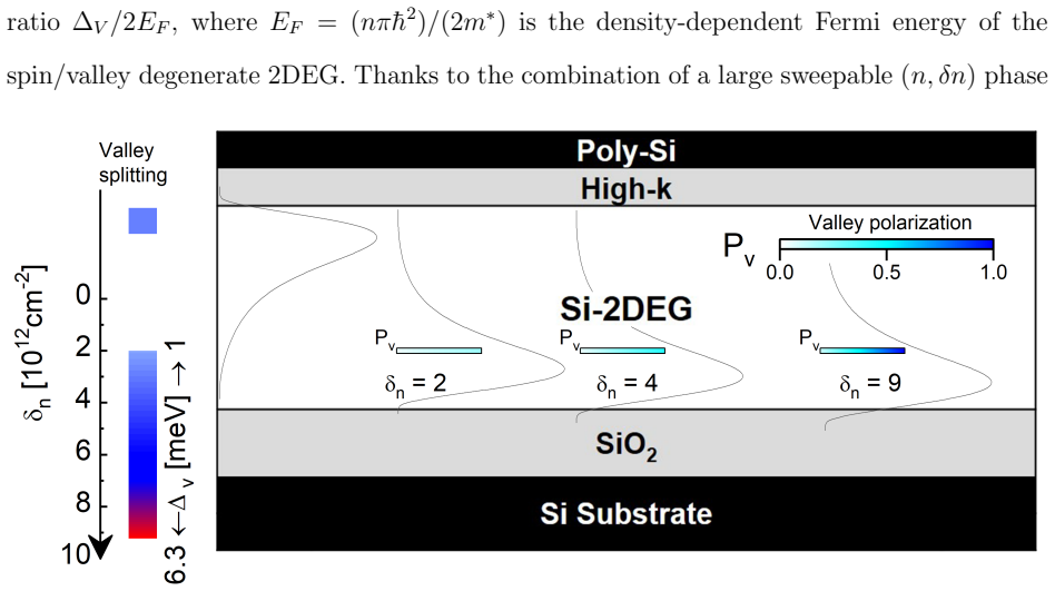
Valley splitting in a [100] silicon quantum well is the energy separation between the two degenerate conduction-band valleys, lifted by intervalley scattering at the confining interface. The paper's control parameter is the electrostatic bias δn = nB − nF, which is shown to control the wavefunction modulus at the interface |Ψ(zi)|^2 and its penetration ∫Ψ(z>zi)^2 dz. The extraction machinery is the Landau-level coincidence/precoincidence method, which converts resistance features into comparisons of cyclotron, spin, and valley gaps. The proportionality of |Ψ(zi)|^2 and the barrier penetration to δn, independent of n, is what makes δn the natural knob.
What would settle it
A sample with the same Si/SiO2 interface but substantially lower disorder, measured at fixed δn while sweeping n over the accessible range, would falsify the independence claim if ΔV changes with n. Alternatively, an independent gap measurement such as thermal activation of resistance minima at one δn that disagrees with the precoincidence-extracted ΔV would question the absolute scale.
Extended reading notes
Core claim
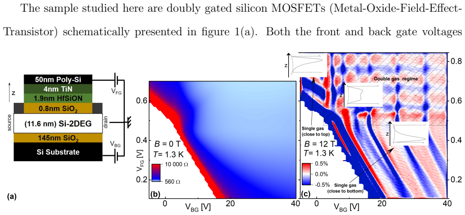
At low temperatures and in magnetic fields, the authors track longitudinal resistance in the quantum Hall regime while independently sweeping front- and back-gate voltages. They convert gate voltages to three quantities: total electron density n = nF + nB, electrostatic bias δn = nB − nF, and the perpendicular and total magnetic fields. When a spin and valley Landau level coincide, the resistance pattern changes, and the paper uses these 'precoincidences' to extract the valley gap ΔV. The central result is a monotonic increase of ΔV with δn, up to 6.3 meV at δn ≈ 9.2 × 10^12 cm^-2, with points at the same δn but different n giving nearly equal ΔV. Poisson-Schrödinger simulations show that at
Load-bearing premise
The reported energy gaps rest on identifying 'precoincidences' in disordered transport and converting them to valley splittings using a disorder model; if that model is wrong, or if the selected precoincidences are unrepresentative, the absolute values and the claimed independence from total density could be off.
Editorial extensions
If this is right
- Electrostatic bias δn, not total density, is the control parameter for valley splitting in doubly gated silicon quantum wells; this allows independent tuning of valley energy while keeping carrier concentration fixed.
- Valley splittings up to 6.3 meV at the buried thermal-oxide interface are reachable, while the same sample can show smaller splittings near the high-k interface, giving a single-device range from roughly 1–2 meV to 6.3 meV.
- Comparisons of valley splitting across different silicon systems should use the interface wavefunction modulus and barrier penetration as the relevant variables rather than raw electric field or density.
- Because the valley splitting can approach a sizable fraction of the Fermi energy, gate-bias control can produce large valley polarization at low temperatures.
- The double-gas regime could host two spatially distinct 2DEGs with different valley splittings in one device, a possible building block for valley-based devices.
Reading between the lines
- If the mapping from δn to |Ψ(zi)|^2 is universal, singly gated MOSFET data should collapse onto the same ΔV versus |Ψ(zi)|^2 trend once their wavefunctions are computed, making the comparison a quantitative test of the underlying theory.
- A direct test would be to vary the barrier material or thickness while keeping δn fixed: the theory predicts the splitting should follow the calculated penetration into the barrier, not the gate voltages themselves.
- The different slopes seen between samples imply that a single universal curve may not exist; each interface may need its own microscopic parameter, which could be probed by controlled interface roughness or strain.
- One could use the demonstrated tunability to operate a single device as a switch between nearly unpolarized and strongly valley-polarized regimes.
Signed reviews
Editorial analysis
A structured set of objections, weighed in public.
Referee Report
Summary. This manuscript reports low-temperature magnetotransport measurements on doubly-gated silicon-on-insulator quantum wells. Using the quantum Hall coincidence method, the authors extract the valley splitting Δv and show that, at the buried thermal-oxide SiO2 interface, Δv increases with the electrostatic bias δn = n_B − n_F and reaches values as high as 6.3 meV, while being independent of the total carrier density n. They connect δn to the calculated wave-function probability at the interface and its penetration into the barrier, both of which are linear in δn, and compare their results with literature data for other silicon 2DEGs. Smaller valley splittings are reported near the front high-k interface.
Significance. If the quantitative extraction is robust, the paper provides a compelling demonstration of electrical valley-splitting tunability in a technologically relevant SOI platform, with a clean separation of total density and vertical electric field. The strengths include the independent double-gate control, the wide (n, δn) range, the use of tilted-field coincidence measurements, the Poisson-Schrodinger simulations of wave-function quantities, and the cross-system comparison with literature data. However, the central Δv values rely on a 'precoincidence' analysis whose disorder characterization is deferred to the supporting information, which is not included in the arXiv submission. This makes the absolute values and the n-independence claim difficult to assess from the main text alone.
major comments (4)
- [Section III.B of the SI; paragraph 'We now turn to quantitative extraction of Δv'] The central values of Δv are obtained from 'precoincidences', but the main text gives no selection criteria for the 50 analyzed precoincidences, no disorder-broadening parameters, and no explicit formula converting resistance onsets into energy gaps. The reader is referred to Section III.B of the supporting information, which is not included in the arXiv submission. This is load-bearing because the largest reported Δv values occur at the largest δn, exactly where disorder is stated to be largest. Please make the full procedure available to reviewers and report the disorder characterization, selection criteria, and a representative example of the conversion.
- [Fig. 3(a)] No error bars or uncertainty estimates are provided for Δv. The claim that Δv is 'independent of the total carrier concentration' is supported only by colored data points; the scatter at fixed δn is not quantified. Please provide error bars (or an equivalent uncertainty quantification) and, if possible, report the residual n-dependence at fixed δn as a slope with uncertainty.
- [Paragraph 'We now turn to quantitative extraction of Δv'] The manuscript states that disorder increases as the wave function is pushed toward the interface, so locating the true spectral coincidence is nontrivial. The precoincidence method is said to require a 'precise characterization of disorder', but the disorder model is not described in the main text. Because the highest Δv values occur at the highest δn, a systematic error in the disorder model could inflate the apparent δn dependence and artificially collapse the n-independence. Please show how the disorder characterization is validated, how sensitive the extracted Δv values are to the assumed disorder parameters, and how selection bias among precoincidences is excluded.
- [Fig. 3(a)-(c) and SI §IV] The x-axis in Fig. 3(a) is the calculated |Ψ(zi)|², and Figs. 3(b,c) present calculated wave-function quantities, but the simulation parameters (effective masses, barrier heights, numerical method, and input density/gate voltages) are only referenced to Section IV of the SI. Since the quantitative comparison across samples and the claim that |Ψ(zi)|² is linear in δn and independent of n depend on these calculations, please include the simulation details and an estimate of their uncertainty in the main text or a fully available appendix.
minor comments (5)
- [Abstract/Introduction] Typo: 'uncomplete' should be 'incomplete'.
- [Acknowledgments] 'M.O. Georbig' is likely 'M.O. Goerbig'.
- [Fig. 1] The color maps in Fig. 1(b,c) are described with resistance values and percentages in the caption, but the figures themselves do not show color bars. Please add color bars or define the full scale.
- [Fig. 2(b-f)] The 'precoincidence' and 'coincidence' terms are introduced in the text but not defined in a figure legend or in a dedicated equation. Consider adding a schematic of the precoincidence condition and a formal definition, even if the quantitative details are in the SI.
- [References] Ref. 8 is missing the author list; Ref. 12 repeats a similar measurement style but could be more clearly distinguished from Ref. 13 in terms of method and sample type.
Circularity Check
No significant circularity: the valley splitting is measured via the standard coincidence method, and the theoretical quantities are computed independently; self-citations are methodological and comparative, not load-bearing.
full rationale
The central quantitative claim (ΔV up to 6.3 meV, tunable by δn and independent of n) is obtained from the coincidence method, in which ΔV is related to the cyclotron gap Δc and spin gap Δs by known coincidence equations (ν=4N+2: ΔV=Δs; ν=4(N+1): ΔV=Δc−Δs). These gaps are set by the measured B⊥ and Btot, not by any parameter fitted to the valley-splitting trend. The precoincidence analysis corrects for Landau-level broadening using a disorder characterization described in the SI; this is a calibration of the extraction, not a fit of ΔV to δn or to the theory. The theoretical quantities |Ψ(zi)|^2 and barrier penetration are computed by independent Poisson-Schrödinger simulations, and Saraiva et al.'s theory is used only to interpret the observed dependence, not to generate it. The comparison with literature data (including Ref. 20 from the same group) is an external benchmark, not an input to the extraction. Although several references (12, 13, 17, 20) are from the same group, they provide methodological precedent and comparative data; the present measurement is self-contained. The missing SI is a reproducibility concern, not circularity: no equation in the main text defines ΔV in terms of the quantities it is claimed to predict, and no fitted parameter is renamed as a prediction.
Assumptions & free parameters
free parameters (1)
- Disorder broadening parameter (used to locate precoincidence) =
Not stated in main text
assumptions (5)
- domain assumption Quantum Hall transport: Landau level quantization and the relation between filling factor, density, and magnetic field.
- domain assumption Coincidence method: when Landau levels with different spin/valley indices coincide, resistance features mark energy equalities such as Δv = Δs or Δc = Δs + Δv.
- domain assumption Saraiva et al. theory: valley splitting is governed by the wave function modulus at the interface and its penetration into the barrier.
- domain assumption Poisson-Schrodinger simulations accurately model the wave function profile in the device given layer structure and gate voltages.
- domain assumption The mapping from (VFG, VBG) to (n, δn) described in SI section II.C is valid.
Cite this review
Pith. "Pith review of Wide Electrical Tunability of the Valley Splitting in a Doubly gated Silicon-on-Insulator Quantum Well." pith.science (2026). https://pith.science/paper/2I7KI6V7
@misc{pith2026250902094,
  author       = {Pith},
  title        = {Pith review of: Wide Electrical Tunability of the Valley Splitting in a Doubly gated Silicon-on-Insulator Quantum Well},
  year         = {2026},
  howpublished = {\url{https://pith.science/paper/2I7KI6V7}},
  note         = {Machine review of arXiv:2509.02094}
}
abstract
The valley splitting of 2D electrons in doubly-gated silicon-on-insulator quantum wells is studied by low temperature transport measurements under magnetic fields. At the buried thermal-oxide SiO$_{2}$ interface, the valley splitting increases as a function of the electrostatic bias $\delta n = n_{B}-n_{F}$ (where $n_{B}$ and $n_{F}$ are electron densities contributed by back and front gates, respectively) and reaches values as high as $6.3$~meV, independent of the total carrier concentration of the channel. We show that $\delta n$ tunes the square of the wave function modulus at the interface and its penetration into the barrier, both of which are key quantities in a theory describing interface-induced valley splitting, and is therefore the natural experimental parameter to manipulate valleys in 2D silicon systems. At the front interface, made of a thin ``high-k'' dielectric, a smaller valley splitting is observed, adding further options to tune the valley splitting within a single device.
Figures


Figures from the paper (1 more)
Reference graph
Works this paper leans on
-
[1]
Review of performance metrics of spin qubits in gated semiconducting nanostructures
Stano, P.; Loss, D. Review of performance metrics of spin qubits in gated semiconducting nanostructures. Nature Reviews Physics 2022, 4, 672--688
work page 2022
-
[2]
Burkard, G.; Ladd, T. D.; Pan, A.; Nichol, J. M.; Petta, J. R. Semiconductor spin qubits. Rev. Mod. Phys. 2023, 95, 025003
work page 2023
-
[3]
J. Ohkawa, F.; Uemura, Y. Theory of Valley Splitting in an N-Channel (100) Inversion Layer of Si III. Enhancement of Splittings by Many-Body Effects. Journal of the Physical Society of Japan 1977, 43, 925--932
work page 1977
-
[4]
Paquelet Wuetz, B. et al. Atomic fluctuations lifting the energy degeneracy in Si/SiGe quantum dots. Nature Communications 2022, 13, 7730
work page 2022
-
[5]
Losert, M. P.; Eriksson, M. A.; Joynt, R.; Rahman, R.; Scappucci, G.; Coppersmith, S. N.; Friesen, M. Practical strategies for enhancing the valley splitting in Si/SiGe quantum wells. Phys. Rev. B 2023, 108, 125405
work page 2023
-
[6]
Enhanced valley splitting in Si layers with oscillatory Ge concentration
Feng, Y.; Joynt, R. Enhanced valley splitting in Si layers with oscillatory Ge concentration. Phys. Rev. B 2022, 106, 085304
work page 2022
-
[7]
Valley-Free Silicon Fins Caused by Shear Strain
Adelsberger, C.; Bosco, S.; Klinovaja, J.; Loss, D. Valley-Free Silicon Fins Caused by Shear Strain. Phys. Rev. Lett. 2024, 133, 037001
work page 2024
-
[8]
Friesen, M.; Chutia, S.; Tahan, C.; Coppersmith, S. N. Phys. Rev. B 2007, 75, 115318
work page 2007
Show all 21 references
-
[9]
L.; Calder\'on, M
Saraiva, A. L.; Calder\'on, M. J.; Hu, X.; Das Sarma, S.; Koiller, B. Physical mechanisms of interface-mediated intervalley coupling in Si. Phys. Rev. B 2009, 80, 081305
2009
-
[10]
Solid State Communications 1980, 34, 51--55
Nicholas, R.; von Klitzing , K.; Englert, T. Solid State Communications 1980, 34, 51--55
1980
-
[11]
S.; Scappucci, G
Lodari, M.; Lampert, L.; Zietz, O.; Pillarisetty, R.; Clarke, J. S.; Scappucci, G. Valley Splitting in Silicon from the Interference Pattern of Quantum Oscillations. Phys. Rev. Lett. 2022, 128, 176603
2022
-
[12]
Valley splitting control in SiO _ 2 / Si/SiO _ 2 quantum wells in the quantum Hall regime
Takashina, K.; Fujiwara, A.; Horiguchi, S.; Takahashi, Y.; Hirayama, Y. Valley splitting control in SiO _ 2 / Si/SiO _ 2 quantum wells in the quantum Hall regime. Phys. Rev. B 2004, 69, 161304
2004
-
[13]
Valley Polarization in Si(100) at Zero Magnetic Field
Takashina, K.; Ono, Y.; Fujiwara, A.; Takahashi, Y.; Hirayama, Y. Valley Polarization in Si(100) at Zero Magnetic Field. Phys. Rev. Lett. 2006, 96, 236801
2006
-
[14]
N.; Elsayed, A.; Mohiyaddin, F
Camenzind, T. N.; Elsayed, A.; Mohiyaddin, F. A.; Li, R.; Kubicek, S.; Jussot, J.; Dorpe, P. V.; Govoreanu, B.; Radu, I.; Zumbühl, D. M. High mobility SiMOSFETs fabricated in a full 300 mm CMOS process. Materials for Quantum Technology 2021, 1, 041001
2021
-
[15]
Intersubband Scattering in Double-Gate MOSFETs
Takashina, K.; Ono, Y.; Fujiwara, A.; Takahashi, Y.; Hirayama, Y. Intersubband Scattering in Double-Gate MOSFETs. IEEE Transactions on Nanotechnology 2006, 5, 430--435
2006
-
[16]
F.; Stiles, P
Fang, F. F.; Stiles, P. J. Effects of a Tilted Magnetic Field on a Two-Dimensional Electron Gas. Phys. Rev. 1968, 174, 823--828
1968
-
[17]
T.; Piot, B
Renard, V. T.; Piot, B. A.; Waintal, X.; Fleury, G.; Cooper, D.; Niida, Y.; Tregurtha, D.; Fujiwara, A.; Hirayama, Y.; Takashina, K. Valley polarization assisted spin polarization in two dimensions. Nat Commun 2015, 6, 7230
2015
-
[18]
A.; Maude, D
Piot, B. A.; Maude, D. K.; Henini, M.; Wasilewski, Z. R.; Friedland, K. J.; Hey, R.; Ploog, K. H.; Toropov, A. I.; Airey, R.; Hill, G. Quantum Hall ferromagnet at high filling factors: A magnetic-field-induced Stoner transition. Phys. Rev. B 2005, 72, 245325
2005
-
[19]
S.; Shashkin, A
Khrapai, V. S.; Shashkin, A. A.; Dolgopolov, V. T. Strong enhancement of the valley splitting in a two-dimensional electron system in silicon. Phys. Rev. B 2003, 67, 113305
2003
-
[20]
T.; Fujiwara, A.; Fujisawa, T.; Muraki, K.; Hirayama, Y
Takashina, K.; Niida, Y.; Renard, V. T.; Fujiwara, A.; Fujisawa, T.; Muraki, K.; Hirayama, Y. Impact of Valley Polarization on the Resistivity in Two Dimensions. Phys. Rev. Lett. 2011, 106, 196403
2011
-
[21]
Valley splitting by extended zone effective mass approximation incorporating strain in silicon
Noborisaka, J.; Hayashi, T.; Fujiwara, A.; Nishiguchi, K. Valley splitting by extended zone effective mass approximation incorporating strain in silicon. Journal of Applied Physics 2024, 135, 204302 mcitethebibliography document
2024
Reviewed August 5, 2026 · model on record in the stance chip above.
Discussion (0). Continue with ORCID to comment.