A deterministic approach for integrating an emitter in a nanocavity with subwavelength light confinement
Pith reviewed 2026-05-16 20:43 UTC · model grok-4.3
The pith
A buried heterostructure emitter integrated into a dielectric bowtie nanocavity achieves coupling strengths of 0.4-0.7 meV at 10-50 nm gaps by co-localizing the optical hotspot and electronic wavefunction.
A machine-rendered reading of the paper's core claim, the machinery that carries it, and where it could break.
Core claim
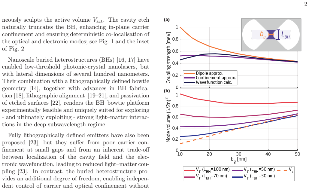
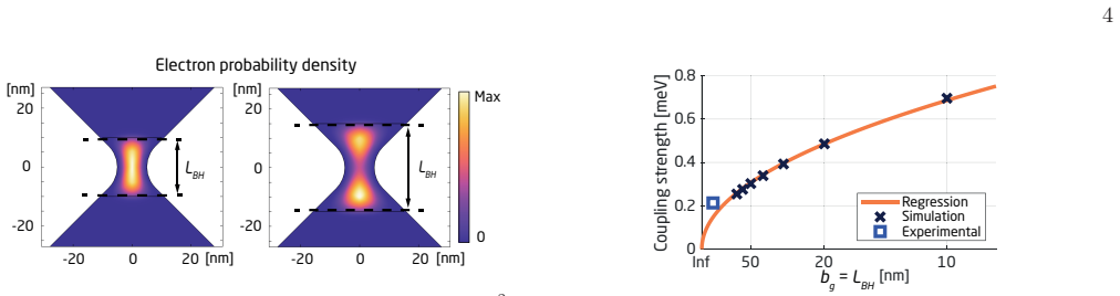
The buried heterostructure-bowtie architecture co-localizes the optical hotspot and the electronic wavefunction inside a dielectric nanocavity. Explicit inclusion of the emitter's finite spatial extent in the confinement-factor approximation produces coupling strengths of 0.4-0.7 meV for gap sizes of 50-10 nm in an InP/InGaAsP system. This supplies design rules inaccessible to point-dipole metrics and demonstrates compatibility with scalable fabrication for deterministic strong coupling.
What carries the argument
The confinement-factor approximation that incorporates the finite spatial extent of the buried heterostructure emitter, which calculates the coupling strength directly from the overlap between the optical mode and the electronic wavefunction.
If this is right
- Strong light-matter interaction occurs through deep subwavelength confinement in a dielectric cavity.
- The platform remains compatible with scalable fabrication methods.
- Design rules for the cavity geometry become accessible that are not captured by dipole-based metrics.
- Deterministic placement of the emitter inside the hotspot enables controlled strong-coupling regimes.
Where Pith is reading between the lines
- The same integration method could be applied to other semiconductor material systems to target different emission wavelengths.
- Electrical gating of the buried heterostructure might allow tuning of the coupling strength in fabricated devices.
- Direct measurement of the predicted coupling values in a 10 nm gap device would confirm the advantage of the confinement-factor approach over dipole approximations.
Load-bearing premise
The numerical models using the confinement-factor approximation that includes the emitter's spatial extent reliably predict the coupling strength without experimental validation.
What would settle it
Fabricating a device with a 10 nm gap and measuring a coupling strength outside the 0.4-0.7 meV range would falsify the prediction.
Figures
read the original abstract
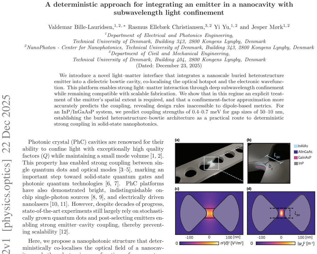
We introduce a novel light-matter interface that integrates a nanoscale buried heterostructure emitter into a dielectric bowtie cavity, co-localising the optical hotspot and the electronic wavefunction. This platform enables strong light-matter interaction through deep subwavelength confinement while remaining compatible with scalable fabrication. We show that in this regime an explicit treatment of the emitter's spatial extent is required, and that a confinement-factor approximation more accurately predicts the coupling, revealing design rules inaccessible to dipole-based metrics. For an InP/InGaAsP system, we predict coupling strengths of 0.4-0.7 meV for gap sizes of 50-10 nm, establishing the buried heterostructure-bowtie architecture as a practical route to deterministic strong coupling in solid-state nanophotonics.
Editorial analysis
A structured set of objections, weighed in public.
Referee Report
Summary. The manuscript introduces a buried-heterostructure InP/InGaAsP emitter integrated into a dielectric bowtie nanocavity that co-localizes the optical hotspot with the electronic wavefunction. It argues that an explicit confinement-factor treatment, rather than a point-dipole approximation, is required when the emitter has finite spatial extent, and reports numerical predictions of vacuum Rabi coupling strengths g = 0.4–0.7 meV for gap sizes 10–50 nm, positioning the architecture as a scalable route to deterministic strong coupling in solid-state nanophotonics.
Significance. If the reported coupling values prove robust, the work would supply concrete design rules for subwavelength light-matter interfaces that remain compatible with standard epitaxial and lithographic processing, potentially accelerating experimental realization of strong-coupling regimes in quantum-dot or quantum-well nanophotonics.
major comments (2)
- [Abstract and §3] Abstract and §3 (numerical results): the headline claim of g = 0.4–0.7 meV rests on an unshown confinement-factor integral that incorporates the finite InGaAsP emitter volume. No mesh-convergence data, FDTD/FEM discretization parameters, material-dispersion model, or comparison against a full Maxwell solution with the actual quantum-well wavefunction are supplied, leaving the quantitative accuracy of the approximation unverified.
- [§4] §4 (discussion of design rules): the assertion that the confinement-factor approach reveals design rules inaccessible to dipole metrics is load-bearing for the paper’s novelty claim, yet no explicit side-by-side comparison (e.g., g_dipole vs. g_confined for the same geometry) or sensitivity analysis to emitter position/orientation is presented.
minor comments (1)
- [Figures] Figure captions and axis labels should explicitly state the assumed emitter dimensions, refractive indices, and gap-size definition used in the simulations.
Simulated Author's Rebuttal
We thank the referee for the constructive comments, which help us strengthen the computational validation and comparative analysis in the manuscript. We address each major point below and will revise the manuscript accordingly.
read point-by-point responses
-
Referee: [Abstract and §3] Abstract and §3 (numerical results): the headline claim of g = 0.4–0.7 meV rests on an unshown confinement-factor integral that incorporates the finite InGaAsP emitter volume. No mesh-convergence data, FDTD/FEM discretization parameters, material-dispersion model, or comparison against a full Maxwell solution with the actual quantum-well wavefunction are supplied, leaving the quantitative accuracy of the approximation unverified.
Authors: We agree that additional details are needed to substantiate the reported coupling values. In the revised manuscript we will explicitly display the confinement-factor integral, supply mesh-convergence data, list the FDTD discretization parameters, specify the material dispersion model for InP/InGaAsP, and provide a direct comparison against a full Maxwell solution that incorporates the finite quantum-well wavefunction. These additions will confirm the accuracy of the 0.4–0.7 meV range for the 10–50 nm gap sizes. revision: yes
-
Referee: [§4] §4 (discussion of design rules): the assertion that the confinement-factor approach reveals design rules inaccessible to dipole metrics is load-bearing for the paper’s novelty claim, yet no explicit side-by-side comparison (e.g., g_dipole vs. g_confined for the same geometry) or sensitivity analysis to emitter position/orientation is presented.
Authors: We concur that a direct comparison is required to support the novelty claim. The revised manuscript will include a side-by-side table and figures contrasting g values computed with the confinement-factor treatment versus the point-dipole approximation for the same bowtie geometries. We will also add a sensitivity analysis showing the dependence of the coupling on emitter position and orientation within the cavity, thereby demonstrating the design rules that become accessible only when the emitter’s spatial extent is accounted for. revision: yes
Circularity Check
No circularity: predictions arise from independent numerical modeling
full rationale
The derivation uses standard electromagnetic confinement-factor calculations on an InP/InGaAsP buried-heterostructure bowtie geometry to obtain coupling values 0.4-0.7 meV. These outputs are not defined in terms of themselves, nor are any fitted parameters relabeled as predictions. No load-bearing self-citations, uniqueness theorems, or ansatz smuggling appear in the provided chain; the confinement-factor treatment is presented as an explicit, externally motivated approximation rather than a tautology. The result is therefore self-contained against external benchmarks.
Axiom & Free-Parameter Ledger
axioms (2)
- standard math Maxwell's equations and standard boundary conditions govern the electromagnetic field distribution inside the dielectric bowtie cavity
- domain assumption The buried heterostructure emitter possesses a finite spatial extent that must be integrated explicitly rather than approximated as a point dipole
Lean theorems connected to this paper
-
IndisputableMonolith/Cost/FunctionalEquation.leanwashburn_uniqueness_aczel unclear?
unclearRelation between the paper passage and the cited Recognition theorem.
yielding ℏg = d (êp · êc) √(ℏωc / 2ε0εr,act) √(Γ / Vact), under the assumption of a uniform carrier distribution (χ=1/Vact inside the emitter)
What do these tags mean?
- matches
- The paper's claim is directly supported by a theorem in the formal canon.
- supports
- The theorem supports part of the paper's argument, but the paper may add assumptions or extra steps.
- extends
- The paper goes beyond the formal theorem; the theorem is a base layer rather than the whole result.
- uses
- The paper appears to rely on the theorem as machinery.
- contradicts
- The paper's claim conflicts with a theorem or certificate in the canon.
- unclear
- Pith found a possible connection, but the passage is too broad, indirect, or ambiguous to say the theorem truly supports the claim.
Reference graph
Works this paper leans on
-
[1]
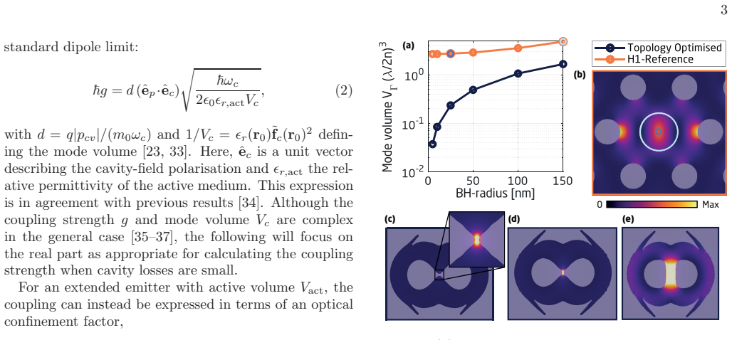
26(λ/ 2n)3 for 20 nm bowtie gaps in III–V semicon- ductors [14] and even smaller in silicon, where bowtie gap sizes below 10 nm have been realised [13]. Further- more, proposed bowtie and slit geometries are compatible with deterministic nanobeam design flows based on the mix-and-match approach [48], where bowtie nanobeam cavities with quality factors abov...
- [2]
-
[3]
G. Crosnier, D. Sanchez, A. Bazin, P. Monnier, S. Bou- choule, R. Braive, G. Beaudoin, I. Sagnes, R. Raj, and F. Raineri, Opt. Lett. 41, 579 (2016)
work page 2016
-
[4]
J. P. Reithmaier, G. Sek, A. L¨ offler, C. Hof- mann, S. Kuhn, S. Reitzenstein, L. V. Keldysh, V. D. Kulakovskii, T. L. Reinecke, and A. Forchel, Nature 432, 197 (2004)
work page 2004
- [5]
-
[6]
R. Ohta, Y. Ota, M. Nomura, N. Kuma- gai, S. Ishida, S. Iwamoto, and Y. Arakawa, Applied Physics Letters 98, 173104 (2011)
work page 2011
-
[7]
J. L. O’Brien, A. Furusawa, and J. Vuˇ ckovi´ c, Nature Photonics 3, 687 (2009)
work page 2009
-
[8]
H. Le Jeannic, A. Tiranov, J. Carolan, T. Ramos, Y. Wang, M. H. Appel, S. Scholz, A. D. Wieck, A. Ludwig, N. Rotenberg, L. Midolo, J. J. Garc ´ ıa-Ripoll, A. S. Sørensen, and P. Lodahl, Nature Physics 18, 1191 (2022)
work page 2022
- [9]
-
[10]
F. Liu, A. J. Brash, J. O’Hara, L. M. P. P. Martins, C. L. Phillips, R. J. Coles, B. Royall, E. Clarke, C. Bentham, N. Prtljaga, I. E. Itskevich, L. R. Wilson, M. S. Skolnick, and A. M. Fox, Nature Nanotechnology 13, 835 (2018)
work page 2018
-
[11]
K.-Y. Jeong, Y.-S. No, Y. Hwang, K. S. Kim, M.-K. Seo, H.-G. Park, and Y.-H. Lee, Nature Communications 4, 2822 (2013)
work page 2013
-
[12]
E. Dimopoulos, M. Xiong, A. Sakanas, A. Marchevsky, G. Dong, Y. Yu, E. Semenova, J. Mørk, and K. Yvind, Optica 10, 973 (2023)
work page 2023
- [13]
-
[14]
M. Albrechtsen, B. V. Lahijani, R. E. Christiansen, V. T. H. Nguyen, L. N. Casses, S. E. Hansen, N. Stenger, O. Sigmund, H. Jansen, J. Mørk, and S. Stobbe, Nature Communications 13, 6281 (2022)
work page 2022
- [15]
-
[16]
G. Khitrova, H. M. Gibbs, M. Kira, S. W. Koch, and A. Scherer, Nature Physics 2, 81 (2006)
work page 2006
- [17]
-
[18]
Sakanas, PhD Thesis, Technical University of Den- mark (2019)
A. Sakanas, PhD Thesis, Technical University of Den- mark (2019)
work page 2019
-
[19]
V. Bille-Lauridsen, M. Xiong, Y. Yu, P. Holewa, E. Semenova, K. Yvind, and J. Mørk, in 2025 CLEO/Europe-EQEC (2025)
work page 2025
- [20]
- [21]
- [22]
-
[23]
Efficient passivation of III-As(P) photonic interfaces,
Y. Berdnikov, P. Holewa, A. Sakanas, J. M. ´Smigiel, P. Mrowi´ nski, E. Zieba-Ost´ oj, K. Yvind, A. Huck, M. Syperek, and E. Semenova, “Efficient passivation of III-As(P) photonic interfaces,” (2025), arXiv:2502.08616 [physics]
-
[24]
G. Kountouris, A. S. Darket, L. Vestergaard, E. V. Denning, J. Mørk, and P. T. Kristensen, Physical Review B 110, L241301 (2024)
work page 2024
-
[25]
J. Y. Marzin, J. M. G´ erard, A. Izra¨ el, D. Barrier, and G. Bastard, Phys. Rev. Lett. 73, 716 (1994)
work page 1994
- [26]
- [27]
- [28]
- [29]
-
[30]
C. Schneider, T. Heindel, A. Huggenberger, P. Weinmann, C. Kistner, M. Kamp, S. Re- itzenstein, S. H¨ ofling, and A. Forchel, Applied Physics Letters 94, 111111 (2009)
work page 2009
-
[31]
P. J. Poole, D. Dalacu, J. Lefebvre, and R. L. Williams, Nanotechnology 21, 295302 (2010)
work page 2010
- [32]
-
[33]
A nanolaser with extreme dielectric confinement,
M. Xiong, Y. Yu, Y. Berdnikov, S. K. Borregaard, A. H. Dubr´ e, E. Semenova, K. Yvind, and J. Mørk, “A nanolaser with extreme dielectric confinement,” (2025)
work page 2025
-
[34]
P. T. Kristensen and S. Hughes, ACS Photonics 1, 2 (2014)
work page 2014
-
[35]
M. Abutoama, G. Kountouris, J. Mørk, and P. T. Kris- tensen, Physical Review B 110, 195434 (2024)
work page 2024
-
[36]
P. T. Kristensen, C. Van Vlack, and S. Hughes, Optics Letters 37, 1649 (2012)
work page 2012
-
[37]
K. G. Cogn´ ee, W. Yan, F. La China, D. Balestri, F. In- tonti, M. Gurioli, A. F. Koenderink, and P. Lalanne, Optica 6, 269 (2019)
work page 2019
-
[38]
O. Bleu, K. Choo, J. Levinsen, and M. M. Parish, Physical Review A 109, 023707 (2024)
work page 2024
-
[39]
M. Saldutti, Y. Yu, and J. Mørk, Laser & Photonics Reviews 18, 2300840 (2024)
work page 2024
-
[40]
L. A. Coldren, S. W. Corzine, and M. L. Maˇ sanovi´ c, Diode Lasers and Photonic Integrated Circuits , 2nd ed., Wiley Series in Microwave and Optical Engineering (John Wiley & Sons, Hoboken, NJ, 2012)
work page 2012
-
[41]
A. Gondarenko, S. Preble, J. Robinson, L. Chen, H. Lipson, and M. Lipson, Physical Review Letters 96, 143904 (2006)
work page 2006
- [42]
-
[43]
M. P. Bendsøe and O. Sigmund, Topology Optimization (Springer, 2003)
work page 2003
-
[44]
S. Nakayama, S. Ishida, S. Iwamoto, and Y. Arakawa, Applied Physics Letters 98, 171102 (2011)
work page 2011
-
[45]
M. Saldutti, M. Xiong, E. Dimopoulos, Y. Yu, M. Gioan- nini, and J. Mørk, Nanomaterials 11, 3030 (2021)
work page 2021
-
[46]
6.3 , COM- SOL AB, Stockholm, Sweden (2023), www.comsol.com
COMSOL AB, COMSOL Multiphysics ® v. 6.3 , COM- SOL AB, Stockholm, Sweden (2023), www.comsol.com
work page 2023
-
[47]
V. R. Almeida, Q. Xu, C. A. Barrios, and M. Lipson, Optics Letters 29, 1209 (2004)
work page 2004
-
[48]
M. Albrechtsen, B. Vosoughi Lahijani, and S. Stobbe, Optics Express 30, 15458 (2022)
work page 2022
-
[49]
S. I. Halimi, Z. Fu, F. O. Afzal, J. A. Allen, S. Hu, and S. M. Weiss, JOSA B 37, 3401 (2020)
work page 2020
- [50]
-
[51]
N. Vats, S. John, and K. Busch, Phys. Rev. A 65, 043808 (2002)
work page 2002
- [52]
- [53]
-
[54]
H. Haug and S. Koch, Quantum Theory of Opt. and Electron. Prop. of Semicond. , Vol. 47 (World Scientific Publishing Co. Pte. Ltd., 2004)
work page 2004
-
[55]
I. Vurgaftman, J. R. Meyer, and L. R. Ram-Mohan, Journal of Applied Physics 89, 5815 (2001)
work page 2001
-
[56]
R. E. Christiansen and O. Sigmund, JOSA B 38, 496 (2021)
work page 2021
- [57]
-
[58]
X. Fan, T. Takagahara, J. E. Cunningham, and H. Wang, Solid State Communications 108, 857 (1998)
work page 1998
-
[59]
J. Mork and G. L. Lippi, Applied Physics Letters 112, 141103 (2018). END MATTER Derivation of coupling strength In the Coulomb gauge, the light–matter interaction Hamiltonian for a charge q can be written as [50] Hint = q m0 p·A(r), (7) where m0 is the free-electron mass, A(r) is the vector potential and p = −iℏ∇ r is the momentum operator. Within the env...
work page 2018
discussion (0)
Sign in with ORCID, Apple, or X to comment. Anyone can read and Pith papers without signing in.