Controlled dewetting and phase transition hysteresis of VO2 nanostructures
Pith reviewed 2026-05-10 19:25 UTC · model grok-4.3
The pith
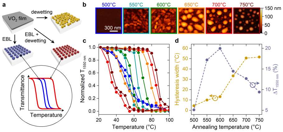
Lithographic patterning, controlled crystallization, and dewetting allow tuning of phase transition hysteresis in VO2 nanocylinders.
A machine-rendered reading of the paper's core claim, the machinery that carries it, and where it could break.
Core claim
Through lithographic patterning to set locations, followed by controlled crystallization and dewetting to define geometry, the phase transition hysteresis of VO2 nanocylinders can be tailored on integrated platforms, extending earlier film-only control methods to structures that consume less power and are simpler to address individually.
What carries the argument
Controlled dewetting during crystallization on lithographically patterned substrates, which sets the nanocylinder geometry that in turn determines the width and position of the hysteresis loop in the optical and electrical response.
If this is right
- Nanocylinders can be produced with geometry-specific hysteresis that matches requirements for short-term memory elements.
- Individual nanostructures become addressable without the crosstalk typical of continuous films.
- Power consumption per switching event drops because only the small cylinder volume undergoes the phase change.
- Direct fabrication on integrated platforms removes the need for separate transfer steps.
- The same process flow can be used to create arrays with deliberately varied transition points for multi-state or analog-like behavior.
Where Pith is reading between the lines
- Arrays of such cylinders could be combined with silicon waveguides to create all-photonic memory banks that operate near room temperature.
- If the dewetting step can be made self-limiting, it might allow wafer-scale production of devices whose transition properties are set purely by layout design rather than post-processing.
- Similar dewetting control might be tested on other hysteretic materials such as certain chalcogenides to broaden the temperature or wavelength range available for neuromorphic optics.
Load-bearing premise
That the tailored hysteresis properties survive integration into actual photonic circuits and that nanostructures will retain their power and addressing advantages once embedded in a full device.
What would settle it
Repeated fabrication runs that produce nanocylinders whose measured hysteresis widths differ by more than the targeted variation, or circuits in which the embedded cylinders lose their designed transition temperatures after packaging and cycling.
Figures


read the original abstract
As artificial intelligence continues to grow, so does the need for more efficient ways to process data. Besides moving from electronic to photonic circuits, a promising approach is to integrate phase-change materials. Vanadium dioxide (VO$_2$) exhibits an ultrafast, near-room-temperature phase transition, characterized by hysteresis and large optical modulation -- making it a promising candidate for short-term memories and for mimicking neural behavior in brain-like computing systems. While the hysteresis behavior of VO$_2$ has been well studied in thin films and nanostructures, practical control and device integration have been limited only to thin films. Here, we demonstrate control over the phase transitions of VO$_2$ nanocylinders via lithographic patterning, controlled crystallization, and controlled dewetting. Because nanostructures are easier to address and consume less power than films, the ability to fabricate them with tailored geometry and hysteresis properties directly on integrated platforms is a key step toward scalable, energy-efficient memory and neuromorphic photonic devices.
Editorial analysis
A structured set of objections, weighed in public.
Referee Report
Summary. The manuscript presents an experimental demonstration of controlling the phase transitions of VO2 nanocylinders via lithographic patterning, controlled crystallization, and controlled dewetting. The authors show that these process steps enable tailored geometry and hysteresis properties in the nanostructures, building on the known ultrafast near-room-temperature phase transition of VO2 with its characteristic hysteresis and optical modulation. The work positions this as a key step toward scalable, energy-efficient memory and neuromorphic photonic devices, noting that nanostructures are easier to address and consume less power than thin films.
Significance. If the experimental results hold, this work would be significant for mesoscopic materials and phase-change photonics. It extends prior studies limited to thin films by providing a fabrication route for geometry-dependent hysteresis control in VO2 nanostructures using standard lithographic and dewetting techniques. This could support integration into photonic circuits for AI applications, where tunable phase transitions enable short-term memory and brain-like computing functions. The approach is promising for reproducibility and device optimization if supported by thorough structural and functional characterization.
minor comments (2)
- The abstract would benefit from a brief quantitative summary of the observed shifts in transition temperature or hysteresis width as a function of nanocylinder geometry or dewetting parameters.
- In the methods and results sections, ensure that the separate contributions of lithographic patterning, crystallization, and dewetting to the final hysteresis are clearly delineated with supporting data from SEM, XRD, and optical/electrical measurements.
Simulated Author's Rebuttal
We thank the referee for the positive summary, significance assessment, and recommendation for minor revision. We are pleased that the potential of controlled dewetting and hysteresis tuning in VO2 nanocylinders for neuromorphic photonic applications is recognized. No specific major comments were provided in the report.
Circularity Check
No circularity: experimental demonstration only
full rationale
The manuscript is a purely experimental report on fabricating VO2 nanocylinders via lithography, crystallization control, and dewetting to tune phase-transition hysteresis. No equations, derivations, fitted parameters, or model predictions appear in the abstract or described workflow. Claims rest on direct fabrication-to-measurement results (SEM, XRD, optical/electrical hysteresis) rather than any self-referential chain. This is the standard case of a self-contained experimental paper with no load-bearing theoretical steps that could reduce to their own inputs.
Axiom & Free-Parameter Ledger
Lean theorems connected to this paper
-
IndisputableMonolith/Cost/FunctionalEquation.leanwashburn_uniqueness_aczel unclear?
unclearRelation between the paper passage and the cited Recognition theorem.
hysteresis width decreases from 56°C at 120 nm diameter to 50°C at 400 nm... fitted by a decreasing exponential function based on the theory of heterogeneous phase transitions
-
IndisputableMonolith/Foundation/AbsoluteFloorClosure.leanabsolute_floor_iff_bare_distinguishability unclear?
unclearRelation between the paper passage and the cited Recognition theorem.
smaller or more pristine VO2 crystals require more supercooling/overheating... because they lack internal defects that can seed the new phase
What do these tags mean?
- matches
- The paper's claim is directly supported by a theorem in the formal canon.
- supports
- The theorem supports part of the paper's argument, but the paper may add assumptions or extra steps.
- extends
- The paper goes beyond the formal theorem; the theorem is a base layer rather than the whole result.
- uses
- The paper appears to rely on the theorem as machinery.
- contradicts
- The paper's claim conflicts with a theorem or certificate in the canon.
- unclear
- Pith found a possible connection, but the passage is too broad, indirect, or ambiguous to say the theorem truly supports the claim.
Reference graph
Works this paper leans on
-
[1]
Lian, C.; Vagionas, C.; Alexoudi, T.; Pleros, N.; Youngblood, N.; Ríos, C. Photonic (com- putational) memories: tunable nanophotonics for data storage and computing.Nanophotonics 2022,11, 3823–3854
work page 2022
-
[2]
Lopez,R.;Haglund,R.F.;Feldman,L.C.;Boatner,L.A.;Haynes,T.E.Opticalnonlinearities in VO2 nanoparticles and thin films.Applied Physics Letters2004,85, 5191–5193
-
[3]
O’Callahan, B. T.; Jones, A. C.; Park, J. H.; Cobden, D. H.; Atkin, J. M.; Raschke, M. B. Inhomogeneityoftheultrafastinsulator-to-metaltransitiondynamicsofVO 2.NatureCommu- nications2015,6, 6849. 14
-
[4]
Morin,F.J.OxidesWhichShowaMetal-to-InsulatorTransitionattheNeelTemperature.Phys. Rev. Lett.1959,3, 34–36
work page 1959
-
[5]
Kepič,P.;Ligmajer,F.;Hrtoň,M.;Ren,H.;deS.Menezes,L.;Maier,S.A.;Šikola,T.Optically Tunable Mie Resonance VO2 Nanoantennas for Metasurfaces in the Visible.ACS Photonics 2021,8, 1048–1057
work page 2021
-
[6]
Jung, Y.; Han, H.; Sharma, A.; Jeong, J.; Parkin, S. S. P.; Poon, J. K. S. Integrated Hybrid VO2–Silicon Optical Memory.ACS Photonics2022,9, 217–223
-
[7]
Parra, J.; Navarro-Arenas, J.; Sanchis, P. Sub-milliwatt Threshold Power and Tunable-Bias All-Optical Nonlinear Activation Function Using Vanadium Dioxide for Wavelength-Division Multiplexing Photonic Neural Networks.Scientific Reports2025,15, 5608
-
[8]
Schofield, P.; Bradicich, A.; Gurrola, R. M.; Zhang, Y.; Brown, T. D.; Pharr, M.; Sham- berger, P. J.; Banerjee, S. Harnessing the Metal–Insulator Transition of VO2 in Neuromorphic Computing.Advanced Materials2023,35, 2205294
-
[9]
J.; Kim, Y.; Gim, H.; Hong, K.; Jang, H
Lee, Y. J.; Kim, Y.; Gim, H.; Hong, K.; Jang, H. W. Nanoelectronics Using Metal–Insulator Transition.Advanced Materials2024,36, 2305353
-
[10]
Rini, M.; Cavalleri, A.; Schoenlein, R. W.; López, R.; Feldman, L. C.; Haglund, R. F.; Boatner, L. A.; Haynes, T. E. Photoinduced Phase Transition in VO2 Nanocrystals: Ultrafast Control of Surface-Plasmon Resonance.Optics Letters2005,30, 558–560
-
[11]
Ryckman, J. D.; Hallman, K. A.; Marvel, R. E.; Haglund, R. F.; Weiss, S. M. Ultra-Compact SiliconPhotonicDevicesReconfiguredbyanOpticallyInducedSemiconductor-to-MetalTran- sition.Optics Express2013,21, 10753–10763
-
[12]
Andrews, J. L.; Santos, D. A.; Meyyappan, M.; Williams, R. S.; Banerjee, S. Building Brain- Inspired Logic Circuits from Dynamically Switchable Transition-Metal Oxides.Trends in Chemistry2019,1, 711–726. 15
-
[13]
Kaufman, M.; Vlček, J.; Houška, J.; Farrukh, S.; Haviar, S. Design and Scalable Synthesis of Thermochromic VO2-Based Coatings for Energy-Saving Smart Windows with Exceptional Optical Performance.ACS Applied Materials & Interfaces2024,16, 57268–57276
-
[14]
White, S. T.; Taylor, J. R.; Chukhryaev, I.; Bailey, S. M.; Queen, J. M.; McBride, J. R.; Haglund,R.F.J.Solid-StateDewettingofTungsten-DopedVanadiumDioxideNanoparticles: Implications for Thermochromic Coatings.ACS Applied Nano Materials2025,8, 9972–9980
-
[15]
ACS Applied Materials & Interfaces2017,9, 1577–1584
Breckenfeld,E.; Kim,H.; Burgess,K.; Charipar,N.; Cheng,S.-F.; Stroud,R.; Piqué,A.Strain EffectsinEpitaxialVO 2ThinFilmsonColumnarBuffer-LayerTiO 2/Al2O3VirtualSubstrates. ACS Applied Materials & Interfaces2017,9, 1577–1584
-
[16]
White, S. T.; Thompson, E. A.; Brown, P. F.; Haglund, R. F. Substrate Chemistry and Lattice Effects in Vapor Transport Growth of Vanadium Dioxide Microcrystals.Crystal Growth and Design2021,21, 3770–3778
-
[17]
Y.; Sonnefraud, Y.; Wang, B.; Pantelides, S
Appavoo, K.; Lei, D. Y.; Sonnefraud, Y.; Wang, B.; Pantelides, S. T.; Maier, S. A.; Haglund, R. F. Role of Defects in the Phase Transition of VO2 Nanoparticles Probed by Plasmon Resonance Spectroscopy.Nano Letters2012,12, 780–786
-
[18]
Lopez, R.; Haynes, T. E.; Boatner, L. A.; Feldman, L. C.; Haglund, R. F. Size effects in the structural phase transition of VO2 nanoparticles.Physical Review B2002,65, 224113
-
[19]
Donev, E. U.; Lopez, R.; Feldman, L. C.; Haglund, R. F. Confocal Raman Microscopy Across TheMetal-InsulatorTransitionofSingleVanadiumDioxideNanoparticles.NanoLetters2009, 9, 702–706
-
[20]
Clarke, H.; Carraway, B. D.; Sellers, D. G.; Braham, E. J.; Banerjee, S.; Arróyave, R.; Shamberger, P. J. Nucleation-controlled hysteresis in unstrained hydrothermal VO2 particles. Physical Review Materials2018,2, 103402. 16
-
[21]
Nishikawa,K.;Nishida,J.;Yoshimura,M.;Nakamoto,K.;Kumagai,T.;Watanabe,Y.Metasta- bility in the Insulator–Metal Transition for Individual Vanadium Dioxide Nanoparticles.The Journal of Physical Chemistry C2023,127, 16485–16495
-
[22]
Kepič, P.; Horák, M.; Kabát, J.; Hájek, M.; Konečná, A.; Šikola, T.; Ligmajer, F. Coexisting Phases of Individual VO2 Nanoparticles for Multilevel Nanoscale Memory.ACS Nano2025, 19, 1167–1176
-
[23]
Griffiths, C. H.; Eastwood, H. K. Influence of Stoichiometry on the Metal–Semiconductor Transition in Vanadium Dioxide.Journal of Applied Physics1974,45, 2201–2206
-
[24]
A Review of Raman Spectroscopy of Vanadium Oxides.Journal of Raman Spectroscopy2019,50, 1226–1244
Shvets, P.; Dikaya, O.; Maksimova, K.; Goikhman, A. A Review of Raman Spectroscopy of Vanadium Oxides.Journal of Raman Spectroscopy2019,50, 1226–1244
-
[25]
Rampelberg, G.; De Schutter, B.; Devulder, W.; Martens, K.; Radu, I.; Detavernier, C. In Situ X-ray Diffraction Study of the Controlled Oxidation and Reduction in the V–O System for the Synthesis of VO2 and V2O3 Thin Films.Journal of Materials Chemistry C2015,3, 11357–11365
-
[26]
Shibuya,K.;Sawa,A.OptimizationofConditionsforGrowthofVanadiumDioxideThinFilms on Silicon by Pulsed-Laser Deposition.AIP Advances2015,5, 107118
-
[27]
Marvel, R. E.; Harl, R. R.; Craciun, V.; Rogers, B. R.; Haglund, R. F. Influence of Deposition ProcessandSubstrateonthePhaseTransitionofVanadiumDioxideThinFilms.ActaMaterialia 2015,91, 217–226
work page 2015
-
[28]
Suh, J. Y.; Lopez, R.; Feldman, L. C.; Haglund, R. F. J. Semiconductor to Metal Phase Transition in the Nucleation and Growth of VO2 Nanoparticles and Thin Films.Journal of Applied Physics2004,96, 1209–1213
-
[29]
Alcaide, A. M.; Regodon, G.; Ferrer, F. J.; Rico, V.; Alvarez, R.; Rojas, T. C.; González- 17 Elipe, A. R.; Palmero, A. Low Temperature Nucleation of Thermochromic VO2 Crystal Do- mains in Nanocolumnar Porous Thin Films.Nanotechnology2023,34, 255702
-
[30]
Marvel, R. E.; Appavoo, K.; Choi, B. K.; Nag, J.; Haglund, R. F. Electron-beam deposition of vanadium dioxide thin films.Applied Physics A2013,111, 975–981
-
[31]
Wen,H.;Guo,L.;Barnes,E.;Lee,J.H.;Walko,D.A.;Schaller,R.D.;Moyer,J.A.;Misra,R.; Li, Y.; Dufresne, E. M.; Schlom, D. G.; Gopalan, V.; Freeland, J. W. Structural and Electronic RecoveryPathwaysofaPhotoexcitedUltrathinVO 2Film.PhysicalReviewB2013,88,165424
-
[32]
M.; Cha, L.; Guo, K.; Wen, S.; Lu, B
Wu, L.; Fu, H.; Li, S.; Zhu, J.; Zhou, J.; Rao, A. M.; Cha, L.; Guo, K.; Wen, S.; Lu, B. Phase- Engineered Cathode for Super-Stable Potassium Storage.Nature Communications2023,14, 644
-
[33]
Li, J.; Navarro, H.; Pofelski, A.; Salev, P.; El Hage, R.; Qiu, E.; Zhu, Y.; Fainman, Y.; Schuller,I.K.Laser-InducedSelectiveLocalPatterningofVanadiumOxidePhases.Advanced Composites and Hybrid Materials2025,8, 157. 18
discussion (0)
Sign in with ORCID, Apple, or X to comment. Anyone can read and Pith papers without signing in.