Atomic-Scale Detection of N\'eel Vector Switching in the Single-Layer A-type Antiferromagnet Cr2S3-2D
Pith reviewed 2026-05-10 17:42 UTC · model grok-4.3
The pith
Substrate-induced moment imbalance enables Néel vector switching in single-layer Cr2S3 antiferromagnet.
A machine-rendered reading of the paper's core claim, the machinery that carries it, and where it could break.
Core claim
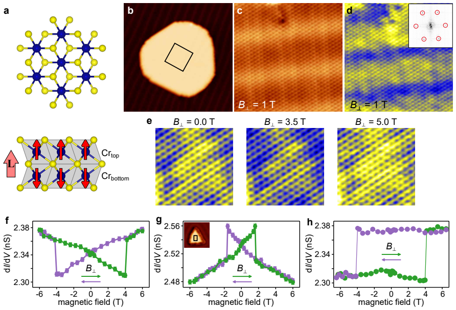
Cr2S3-2D grown on graphene on Ir(110) is a single-layer A-type antiferromagnet in which a substrate-induced imbalance between the moments of the two Cr planes creates a net magnetization. This net moment allows observation of 180° Néel vector switching through large, island-size-dependent hysteresis loops in spin-polarized STM, while XMCD confirms the compensated ground state and air stability.
What carries the argument
The slight imbalance between the magnetic moments of the two Cr planes of Cr2S3-2D when supported on a substrate, which produces a net magnetization enabling 180° Néel vector rotation.
If this is right
- The switching field increases with island size because the net magnetization scales with the number of spins.
- Cr2S3-2D retains its magnetic properties after several days of air exposure.
- The Néel temperature is approximately 160 K from the temperature dependence of the XMCD signal.
- First-principles calculations support the existence of the substrate-induced moment difference.
Where Pith is reading between the lines
- Substrate choice could be used to tune the size of the net moment and thus the switching field in similar 2D antiferromagnets.
- Atomic-resolution STM imaging of the switching process could reveal domain nucleation sites in single-layer systems.
- Air stability suggests the material can be transferred to other substrates without immediate loss of antiferromagnetic order.
Load-bearing premise
The observed hysteresis loops and their island-size dependence arise primarily from a substrate-induced moment imbalance rather than from defects, edge effects, or unmodeled substrate interactions.
What would settle it
A measurement showing no net magnetization or moment imbalance in the supported Cr2S3-2D, or switching fields independent of island size, would falsify the explanation.
Figures


read the original abstract
The detection of N\'eel vector switching in a single-layer A-type antiferromagnet marks an important step toward functional two-dimensional spintronics. Here, Cr$_2$S$_3$-2D, grown on graphene on Ir(110), is established as a first single-layer A-type antiferromagnet. Spin-polarized scanning tunneling microscopy reveals hysteresis loops with a large switching field and a pronounced dependence on island size. X-ray magnetic circular dichroism at the Cr L$_{2,3}$ edges exhibits a tiny signal with a linear magnetic field dependence, consistent with a nearly compensated antiferromagnetic ground state and a N\'eel temperature of about 160 K. Quantitative analysis of the island-size dependence of the switching field, together with first principles calculations, indicates a slight imbalance between the magnetic moments of the two Cr planes of Cr$_2$S$_3$-2D when supported on a substrate. This imbalance results in a net magnetization for the A-type antiferromagnet, which enables the 180$^\circ$ rotation of the N\'eel vector. Moreover, Cr$_2$S$_3$-2D retains its magnetic properties after several days of exposure to air.
Editorial analysis
A structured set of objections, weighed in public.
Referee Report
Summary. The manuscript reports the first observation of Néel-vector switching in a single-layer A-type antiferromagnet, Cr2S3-2D grown on graphene/Ir(110). Spin-polarized STM reveals hysteresis loops with large switching fields that depend strongly on island size; XMCD at the Cr L2,3 edges shows a weak, linear-in-field signal consistent with a nearly compensated state and TN ≈ 160 K. Quantitative modeling of the size-dependent switching field, combined with DFT, is used to infer a small substrate-induced imbalance between the magnetic moments of the two Cr planes; this imbalance is argued to produce a net magnetization that permits 180° Néel-vector rotation under the observed fields. Air stability after several days is also demonstrated.
Significance. If the central interpretation is confirmed, the work constitutes a notable advance for 2D antiferromagnetic spintronics by providing atomic-scale detection of Néel-vector switching in a true single-layer A-type antiferromagnet. The multi-technique approach (SP-STM, XMCD, DFT) and the reported air stability are practical strengths; the size-scaling analysis offers a route to extract the small net moment that would otherwise be inaccessible.
major comments (1)
- [Abstract and the section presenting the size-dependence analysis] The quantitative attribution of the observed island-size dependence of the switching field to a substrate-induced Cr-plane moment imbalance (central claim in the abstract) is load-bearing yet relies on post-experiment modeling whose sensitivity to alternative explanations (defects, edge pinning, or unmodeled graphene/Ir interactions) is not fully quantified. No independent experimental bound on the net moment (e.g., integrated XMCD intensity or SQUID magnetometry) is reported that could be compared directly to the DFT value used in the scaling model.
minor comments (2)
- [XMCD experimental details] Clarify the exact temperature and field range used for the XMCD measurements and state whether the linear field dependence persists above TN.
- [Computational methods] Ensure that the DFT supercell size, substrate model (graphene/Ir(110)), and convergence criteria for the moment imbalance are explicitly tabulated or described.
Simulated Author's Rebuttal
We thank the referee for the careful and constructive review. We address the single major comment below and have revised the manuscript to strengthen the quantitative aspects of the size-dependence analysis.
read point-by-point responses
-
Referee: [Abstract and the section presenting the size-dependence analysis] The quantitative attribution of the observed island-size dependence of the switching field to a substrate-induced Cr-plane moment imbalance (central claim in the abstract) is load-bearing yet relies on post-experiment modeling whose sensitivity to alternative explanations (defects, edge pinning, or unmodeled graphene/Ir interactions) is not fully quantified. No independent experimental bound on the net moment (e.g., integrated XMCD intensity or SQUID magnetometry) is reported that could be compared directly to the DFT value used in the scaling model.
Authors: We agree that the modeling is central and that additional quantification improves the manuscript. The observed switching field scales as 1/A across islands spanning more than an order of magnitude in area, which is the signature expected for coherent rotation driven by a uniform net moment m_net (H_sw = 2K_eff / (m_net * A)). Alternative mechanisms such as random defect pinning or edge effects would produce either larger island-to-island scatter at fixed area or a weaker (or absent) area dependence; neither is seen in the data. We have added a dedicated paragraph and supplementary analysis that (i) tests the robustness of the extracted m_net against ±20% variations in anisotropy and exchange parameters and (ii) explicitly rules out dominant graphene/Ir contributions by comparing DFT results with and without the substrate. For an independent experimental bound, the slope of the linear XMCD signal versus applied field directly constrains the net moment per Cr atom; this experimental value is now compared quantitatively to the DFT imbalance (~0.01–0.02 μ_B/Cr) in the revised text and a new supplementary figure. SQUID magnetometry on individual nanoscale islands is precluded by substrate diamagnetism and signal-to-noise limits, but the XMCD measurement on the same samples provides the requested cross-check. These additions are incorporated in the revised version. revision: yes
Circularity Check
No significant circularity; central claim rests on independent experimental data and first-principles DFT.
full rationale
The paper derives its key result (substrate-induced Cr-plane moment imbalance enabling Néel-vector rotation) from measured island-size dependence of switching fields in SP-STM hysteresis loops, combined with separate first-principles calculations. This chain does not reduce by construction to self-definition, fitted inputs renamed as predictions, or load-bearing self-citations. DFT provides an external ab initio input independent of the experimental observables, and no uniqueness theorem or ansatz is smuggled via prior author work. The derivation remains self-contained against external benchmarks.
Axiom & Free-Parameter Ledger
free parameters (1)
- Cr-plane moment imbalance
axioms (1)
- domain assumption Cr2S3-2D adopts A-type antiferromagnetic order with two Cr planes
Lean theorems connected to this paper
-
IndisputableMonolith/Cost/FunctionalEquation.leanwashburn_uniqueness_aczel unclear?
unclearRelation between the paper passage and the cited Recognition theorem.
Quantitative analysis of the island-size dependence of the switching field, together with first principles calculations, indicates a slight imbalance between the magnetic moments of the two Cr planes
-
IndisputableMonolith/Foundation/RealityFromDistinction.leanreality_from_one_distinction unclear?
unclearRelation between the paper passage and the cited Recognition theorem.
Sharrock-type expression μ0Hsw = 2ΔE/μu [1 − (kBT/ΔE ln(tmeas/τ0))^{1/2}]
What do these tags mean?
- matches
- The paper's claim is directly supported by a theorem in the formal canon.
- supports
- The theorem supports part of the paper's argument, but the paper may add assumptions or extra steps.
- extends
- The paper goes beyond the formal theorem; the theorem is a base layer rather than the whole result.
- uses
- The paper appears to rely on the theorem as machinery.
- contradicts
- The paper's claim conflicts with a theorem or certificate in the canon.
- unclear
- Pith found a possible connection, but the passage is too broad, indirect, or ambiguous to say the theorem truly supports the claim.
Reference graph
Works this paper leans on
- [1]
-
[2]
J. ˇZelezn´ y, P. Wadley, K. Olejn´ ık, A. Hoffmann, and H. Ohno, Spin transport and spin torque in antiferromagnetic devices, Nat. Phys.14, 220 (2018). 16
work page 2018
-
[3]
Z. Guo, X. Wang, W. Wang, G. Zhang, X. Zhou, and Z. Cheng, Spin-polarized antiferromag- nets for spintronics, Adv. Mater.37, 2505779 (2025)
work page 2025
-
[4]
L. Han, X. Fu, R. Peng, X. Cheng, J. Dai, L. Liu, Y. Li, Y. Zhang, W. Zhu, H. Bai, Y. Zhou, S. Liang, C. Chen, Q. Wang, X. Chen, L. Yang, Y. Zhang, C. Song, J. Liu, and F. Pan, Elec- trical 180°switching of N´ eel vector in spin-splitting antiferromagnet, Sci. Adv.10, eadn0479 (2024)
work page 2024
-
[5]
Z. Wang, Y. Xiang, R. Chen, Z. Sun, C. Hong, X. Chen, J. Gao, S. Wu, Z. Guo, Y. Chen, Q. Mi, Z. Liu, S. Yan, H. Lei, W. Ruan, Y. Zhang, W. Yu, W.-T. Liu, Z. Yuan, and S. Wu, Ferromagnet-like binary switching of a Stoner–Wohlfarth antiferromagnet, Nature650, 340 (2026)
work page 2026
-
[6]
Y. Liu, C. Zeng, J. Zhong, J. Ding, Z. M. Wang, and Z. Liu, Spintronics in two-dimensional materials, Nano-Micro Lett.12, 93 (2020)
work page 2020
-
[7]
Z. Zhao, Y. Lin, and A. Avsar, Novel spintronic effects in two-dimensional van der Waals heterostructures, npj 2D Mater. Appl.9, 30 (2025)
work page 2025
-
[8]
Z. Jia, M. Zhao, Q. Chen, Y. Tian, L. Liu, F. Zhang, D. Zhang, Y. Ji, B. Camargo, K. Ye, R. Sun, Z. Wang, and Y. Jiang, Spintronic Devices upon 2D Magnetic Materials and Hetero- junctions, ACS Nano19, 9452 (2025)
work page 2025
-
[9]
B. Yang, Y. M. Goh, S. H. Sung, G. Ye, S. Biswas, D. A. S. Kaib, R. Dhakal, S. Yan, C. Li, S. Jiang, F. Chen, H. Lei, R. He, R. Valent´ ı, S. M. Winter, R. Hovden, and A. W. Tsen, Magnetic anisotropy reversal driven by structural symmetry-breaking in monolayerα-RuCl 3, Nat. Mater.22, 50 (2023)
work page 2023
-
[10]
J.-J. Xian, C. Wang, J.-H. Nie, R. Li, M. Han, J. Lin, W.-H. Zhang, Z.-Y. Liu, Z.-M. Zhang, M.-P. Miao, Y. Yi, S. Wu, X. Chen, J. Han, Z. Xia, W. Ji, and Y.-S. Fu, Spin mapping of intralayer antiferromagnetism and field-induced spin reorientation in monolayer CrTe 2, Nat. Commun.13, 257 (2022)
work page 2022
-
[11]
Z. Ni, A. V. Haglund, H. Wang, B. Xu, C. Bernhard, D. G. Mandrus, X. Qian, E. J. Mele, C. L. Kane, and L. Wu, Imaging the N´ eel vector switching in the monolayer antiferromagnet MnPSe3 with strain-controlled Ising order, Nat. Nanotechnol.16, 782 (2021)
work page 2021
-
[12]
B. Huang, G. Clark, E. Navarro-Moratalla, D. R. Klein, R. Cheng, K. L. Seyler, D. Zhong, E. Schmidgall, M. A. McGuire, D. H. Cobden, W. Yao, D. Xiao, P. Jarillo-Herrero, and X. Xu, Layer-dependent ferromagnetism in a van der waals crystal down to the monolayer 17 limit, Nature546, 270 (2017)
work page 2017
-
[13]
K. Lee, A. H. Dismukes, E. J. Telford, R. A. Wiscons, J. Wang, X. Xu, C. Nuckolls, C. R. Dean, X. Roy, and X. Zhu, Magnetic Order and Symmetry in the 2D Semiconductor CrSBr, Nano Lett.21, 3511 (2021)
work page 2021
-
[14]
D. C. Freitas, R. Weht, A. Sulpice, G. Remenyi, P. Strobel, F. Gay, J. Marcus, and M. N´ u˜ nez- Regueiro, Ferromagnetism in layered metastable 1T-CrTe 2, J. Phys. Condens. Matter.27, 176002 (2015)
work page 2015
-
[15]
N. Kushwaha, O. Armitage, B. Edwards, L. Trzaska, P. Bencok, D. Biswas, T.-L. Lee, C. Sanders, G. van der Laan, P. Wahl, P. D. King, and A. Rajan, From ferromagnetic semi- conductor to antiferromagnetic metal in epitaxial Cr xTey monolayers, npj Quantum Mater. 10, 50 (2025)
work page 2025
-
[16]
K. O. Klepp and H. Ipser, CrTe 3—A Novel Transition-Metal Polytelluride, Angew. Chem., Int. Ed. Engl.21, 911 (1982)
work page 1982
-
[17]
Chattopadhyay, The Cr-Te (Chromium-Tellurium) System, J
G. Chattopadhyay, The Cr-Te (Chromium-Tellurium) System, J. Phase Equilib.15, 431 (1994)
work page 1994
-
[18]
Jellinek, The structures of the chromium sulphides, Acta Crystallogr.10, 620 (1957)
F. Jellinek, The structures of the chromium sulphides, Acta Crystallogr.10, 620 (1957)
work page 1957
-
[19]
F. H. Wehmeier, E. T. Keve, and S. C. Abrahams, Preparation, structure, and properties of some chromium selenides. Crystal growth with selenium vapor as a novel transport agent, Inorg. Chem.9, 2125 (1970)
work page 1970
-
[20]
C.-W. Chuang, T. Kawakami, K. Sugawara, K. Nakayama, S. Souma, M. Kitamura, K. Amemiya, K. Horiba, H. Kumigashira, G. Kremer, Y. Fagot-Revurat, D. Malterre, C. Bigi, F. Bertran, F. H. Chang, H. J. Lin, C. T. Chen, T. Takahashi, A. Chainani, and T. Sato, Spin-valley coupling enhanced high-T C ferromagnetism in a non-van der Waals monolayer Cr2Se3 on graphe...
work page 2025
-
[21]
L. Song, Y. Zhao, R. Du, H. Li, X. Li, W. Feng, J. Yang, X. Wen, L. Huang, Y. Peng, H. Sun, Y. Jiang, J. He, and J. Shi, Coexistence of Ferroelectricity and Ferromagnetism in Atomically Thin Two-Dimensional Cr 2S3/WS2 Vertical Heterostructures, Nano Lett.24, 2408 (2024)
work page 2024
- [22]
-
[23]
Y. Li, Y. Wu, L. Deng, X. Yin, X. Han, F. Tian, and X. Zhang, Spontaneous spin and valley polarizations in a two-dimensional Cr 2S3 monolayer, J. Appl. Phys.133, 134301 (2023)
work page 2023
- [24]
-
[25]
W. Chen, S. Liu, L. Han, J. Yu, J. Xu, M. Shi, X. Li, K. Huang, and P. Li, Exploring the electronic and magnetic properties of two-dimensional M 2X3 (M=V, Cr, Mn, Fe, Co, Ni; X=O, S, Se, Te) compounds, Phys. B: Condens. Matter.714, 417396 (2025)
work page 2025
-
[26]
L. ˇSmejkal, J. Sinova, and T. Jungwirth, Beyond Conventional Ferromagnetism and Antifer- romagnetism: A Phase with Nonrelativistic Spin and Crystal Rotation Symmetry, Phys. Rev. X12, 031042 (2022)
work page 2022
-
[27]
S. Reimers, L. Odenbreit, L. ˇSmejkal, V. N. Strocov, P. Constantinou, A. B. Hellenes, R. Jaeschke Ubiergo, W. H. Campos, V. K. Bharadwaj, A. Chakraborty, T. Denneulin, W. Shi, R. E. Dunin-Borkowski, S. Das, M. Kl¨ aui, J. Sinova, and M. Jourdan, Direct observation of altermagnetic band splitting in CrSb thin films, Nat. Commun.15, 2116 (2024)
work page 2024
- [28]
-
[29]
D. Wortmann, S. Heinze, P. Kurz, G. Bihlmayer, and S. Bl¨ ugel, Resolving Complex Atomic- Scale Spin Structures by Spin-Polarized Scanning Tunneling Microscopy, Phys. Rev. Lett.86, 4132 (2001)
work page 2001
- [30]
- [31]
-
[32]
H. Oka, P. A. Ignatiev, S. Wedekind, G. Rodary, L. Niebergall, V. S. Stepanyuk, D. Sander, and J. Kirschner, Spin-Dependent Quantum Interference Within a Single Magnetic Nanos- tructure, Science327, 843 (2010)
work page 2010
-
[33]
K. Yaji, A. Kimura, C. Hirai, M. Taniguchi, M. Koyama, H. Sato, K. Shimada, A. Tanaka, T. Muro, S. Imada, and S. Suga, Electronic structure of Cr 1-δX(X= S,Te) studied by Cr 2p soft x-ray magnetic circular dichroism, Phys. Rev. B70, 064402 (2004). 19
work page 2004
-
[34]
C. T. Chen, Y. U. Idzerda, H.-J. Lin, N. V. Smith, G. Meigs, E. Chaban, G. H. Ho, E. Pellegrin, and F. Sette, Experimental Confirmation of the X-Ray Magnetic Circular Dichroism Sum Rules for Iron and Cobalt, Phys. Rev. Lett.75, 152 (1995)
work page 1995
-
[35]
A. Bedoya-Pinto, J.-R. Ji, A. K. Pandeya, P. Gargiani, M. Valvidares, P. Sessi, J. M. Taylor, F. Radu, K. Chang, and S. S. P. Parkin, Intrinsic 2D-XY ferromagnetism in a van der Waals monolayer, Science374, 616 (2021)
work page 2021
-
[36]
M. P. Sharrock, Time dependence of switching fields in magnetic recording media (invited), J. Appl. Phys.76, 6413 (1994)
work page 1994
-
[37]
W. Wernsdorfer, Classical and Quantum Magnetization Reversal Studied in Nanometer-Sized Particles and Clusters, In Advances in Chemical Physics (eds I. Prigogine and S.A. Rice) (2001)
work page 2001
-
[38]
F. Hellman, A. Hoffmann, Y. Tserkovnyak, G. S. D. Beach, E. E. Fullerton, C. Leighton, A. H. MacDonald, D. C. Ralph, D. A. Arena, H. A. D¨ urr, P. Fischer, J. Grollier, J. P. Heremans, T. Jungwirth, A. V. Kimel, B. Koopmans, I. N. Krivorotov, S. J. May, A. K. Petford-Long, J. M. Rondinelli, N. Samarth, I. K. Schuller, A. N. Slavin, M. D. Stiles, O. Tchern...
work page 2017
-
[39]
M. Keunecke, F. Lyzwa, D. Schwarzbach, V. Roddatis, N. Gauquelin, K. M¨ uller-Caspary, J. Verbeeck, S. J. Callori, F. Klose, M. Jungbauer, and V. Moshnyaga, High-T C Interfacial Ferromagnetism in SrMnO3/LaMnO3 Superlattices, Adv. Funct. Mater.30, 1808270 (2020)
work page 2020
-
[40]
J. P. Bange, V. Roddatis, L. Sch¨ uler, F. Lyzwa, M. Keunecke, S. Lopatin, V. Bruchmann- Bamberg, and V. Moshnyaga, Charge Transfer Control of Emergent Magnetism at SrMnO3/LaMnO3 Interfaces, Adv. Mater. Interfaces9, 2201282 (2022)
work page 2022
-
[41]
C. Hong, Z. Sun, Z. Sheng, S. Wu, Y. Chen, M. Tian, N. Wan, Q. Mi, Z. Liu, W. Chu, and S. Wu, Charge transfer governed interlayer magnetic coupling and symmetry breaking in a van der Waals magnet, Nat. Commun.16, 9498 (2025)
work page 2025
-
[42]
C. P. Bean and J. D. Livingston, Superparamagnetism, J. Appl. Phys.30, S120 (1959)
work page 1959
- [43]
-
[44]
D. Neˇ cas and P. Klapetek, Gwyddion: an open-source software for SPM data analysis, Cent. Eur. J. Phys.10, 181 (2012)
work page 2012
- [45]
-
[46]
A. Barla, J. Nicol´ as, D. Cocco, S. M. Valvidares, J. Herrero-Mart´ ın, P. Gargiani, J. Moldes, C. Ruget, E. Pellegrin, and S. Ferrer, Design and performance of BOREAS, the beamline for resonant X-ray absorption and scattering experiments at the ALBA synchrotron light source, J. Synchrotron Radiat.23, 1507 (2016)
work page 2016
-
[47]
G. Kresse and D. Joubert, From ultrasoft pseudopotentials to the projector augmented-wave method, Phys. Rev. B59, 1758 (1999)
work page 1999
-
[48]
G. Kresse and J. Furthm¨ uller, Efficient iterative schemes forab initiototal-energy calculations using a plane-wave basis set, Phys. Rev. B54, 11169 (1996)
work page 1996
-
[49]
J. P. Perdew, K. Burke, and M. Ernzerhof, Generalized gradient approximation made simple, Phys. Rev. Lett.77, 3865 (1996)
work page 1996
-
[50]
S. Grimme, Semiempirical gga-type density functional constructed with a long-range disper- sion correction, J. Comput. Chem.27, 1787 (2006)
work page 2006
-
[51]
K. Momma and F. Izumi,VESTA: a three-dimensional visualization system for electronic and structural analysis, J. Appl. Crystallogr.41, 653 (2008). 21 Supplementary Information: Atomic-Scale Detection of Néel Vector Switching in the Single-Layer A-type Antiferromagnet Cr 2S3-2D Affan Safeer,1,∗Calisa Dias,2 Mahdi Ghorbani-Asl,3 Abdallah Karaka,1 Pradyumna ...
work page 2008
discussion (0)
Sign in with ORCID, Apple, or X to comment. Anyone can read and Pith papers without signing in.