Persistence of large and gate-tunable anisotropic magnetoresistance in an atomically thin antiferromagnet
Pith reviewed 2026-05-10 08:17 UTC · model grok-4.3
The pith
Electrical readout of the Néel vector works in two-layer NiPS3 with full gate control over magnetoresistance sign and magnitude.
A machine-rendered reading of the paper's core claim, the machinery that carries it, and where it could break.
Core claim
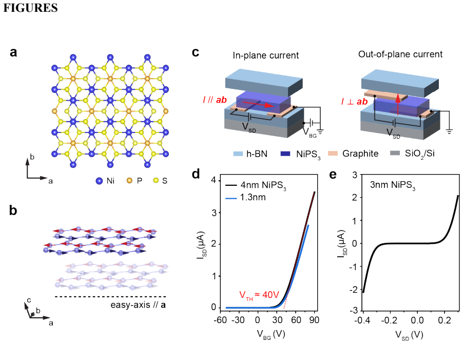
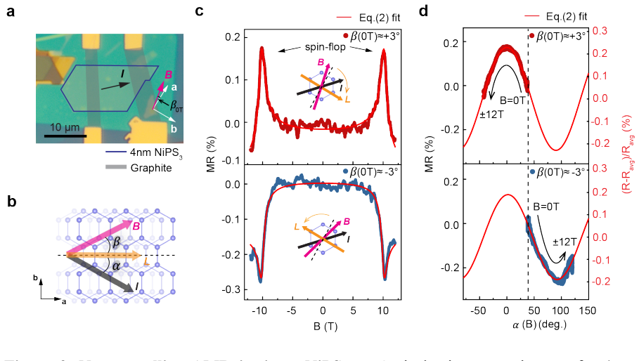
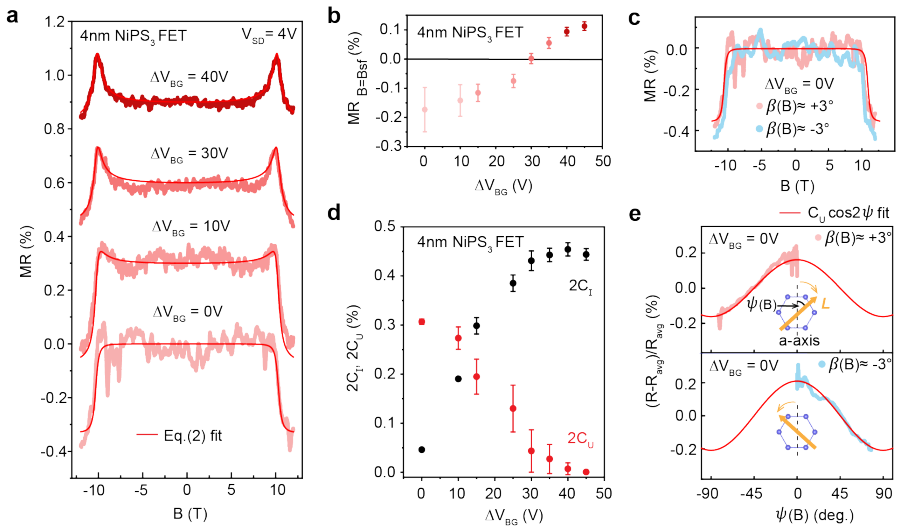
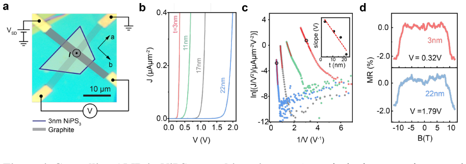
We demonstrate electrical readout of the Néel vector down to 1.3 nm (two layers) in the two-dimensional van der Waals AFM semiconductor NiPS3. Leveraging spin-flop-mediated rotation of the Néel vector and using both transistor and tunnel-junction device geometries, we identify two distinct AMR contributions in NiPS3 that dominate at low and high charge densities, respectively. We achieve full gate control over these contributions, enabling tunability of both the magnitude and sign of magnetoresistance.
What carries the argument
Spin-flop rotation of the Néel vector observed through gate-dependent anisotropic magnetoresistance in transistor and tunnel-junction geometries of NiPS3.
Load-bearing premise
The measured resistance changes arise specifically from rotation of the Néel vector during spin-flop transitions rather than from interface disorder, reduced dimensionality, or unrelated transport mechanisms.
What would settle it
Resistance changes that fail to occur at the magnetic field value required for the spin-flop transition in NiPS3, or that appear equally in non-antiferromagnetic reference samples under identical gating conditions.
Figures
read the original abstract
Anisotropic magnetoresistance (AMR) offers a robust electrical readout of antiferromagnetic (AFM) states, playing a central role in the rapidly advancing field of AFM spintronics. Despite its great versatility, electrical probing of the N\'eel vector via AMR remains challenging in the ultrathin limit due to interface disorder and reduced dimensionality. Here, we demonstrate electrical readout of the N\'eel vector down to 1.3 nm (two layers) in the two-dimensional van der Waals (vdW) AFM semiconductor NiPS3. Leveraging spin-flop-mediated rotation of the N\'eel vector and using both transistor and tunnel-junction device geometries, we identify two distinct AMR contributions in NiPS3, that dominate at low and high charge densities, respectively. We achieve full gate control over these contributions, enabling tunability of both the magnitude and sign of magnetoresistance. Our results establish semiconducting vdW antiferromagnets as a rich platform for studying AMR in the ultrathin limit, opening new avenues for multifunctional AFM spintronic devices.
Editorial analysis
A structured set of objections, weighed in public.
Referee Report
Summary. The manuscript reports experimental observation of anisotropic magnetoresistance (AMR) in atomically thin NiPS3, a 2D van der Waals antiferromagnetic semiconductor. Using both transistor and tunnel-junction device geometries, the authors demonstrate electrical readout of the Néel vector down to two layers (1.3 nm thickness). They identify two distinct AMR contributions that dominate at low and high charge densities, respectively, and show that gate voltage provides full control over the magnitude and sign of the magnetoresistance, which they attribute to spin-flop-mediated rotation of the antiferromagnetic order parameter.
Significance. If the mechanism attribution holds, the work would be significant for AFM spintronics by establishing robust, gate-tunable electrical readout of AFM states in the ultrathin limit of vdW materials, where interface disorder and reduced dimensionality typically complicate such measurements. The dual device geometries and demonstration of sign-tunable AMR provide a versatile platform for multifunctional devices. The experimental focus on few-layer flakes with clear device fabrication details is a strength.
major comments (3)
- [Results on AMR identification in low- and high-density regimes] The central claim that the measured resistance changes arise specifically from spin-flop rotation of the Néel vector (rather than interface disorder, magnetostriction, or dimensionality effects independent of long-range AFM order) is load-bearing but insufficiently secured. The manuscript does not present temperature-dependent AMR data that tracks the known AFM transition temperature of NiPS3 or thickness-dependent critical fields for the spin-flop transition.
- [Gate-tunability and mechanism discussion] The separation into two AMR contributions by charge-density regime and their attribution to the same spin-flop mechanism requires additional controls. Explicit comparison to non-magnetic isostructural analogs or measurements showing that the AMR vanishes above the AFM ordering temperature would be needed to exclude alternative magnetotransport mechanisms.
- [Device geometries and transport data] While gate control over magnitude and sign is demonstrated, the robustness of the effect across devices is not quantified. Inclusion of statistics from multiple devices, error bars on all ΔR data, and field-sweep hysteresis loops confirming the spin-flop signature would strengthen the conclusions.
minor comments (1)
- [Figures and captions] Ensure all figures include scale bars, error bars where applicable, and clear labeling of layer thicknesses and gate voltages for reproducibility.
Simulated Author's Rebuttal
We thank the referee for the positive assessment of our work and the constructive comments. We have carefully revised the manuscript to address the concerns about securing the AMR mechanism attribution, providing additional controls, and quantifying device robustness. Our point-by-point responses are as follows.
read point-by-point responses
-
Referee: The central claim that the measured resistance changes arise specifically from spin-flop rotation of the Néel vector (rather than interface disorder, magnetostriction, or dimensionality effects independent of long-range AFM order) is load-bearing but insufficiently secured. The manuscript does not present temperature-dependent AMR data that tracks the known AFM transition temperature of NiPS3 or thickness-dependent critical fields for the spin-flop transition.
Authors: We agree that direct evidence linking the AMR to the AFM order is crucial. In the revised manuscript, we have added temperature-dependent AMR measurements (Supplementary Figure S5) demonstrating that the anisotropic magnetoresistance signal disappears above the Néel temperature of the thin NiPS3 flakes, consistent with the loss of long-range AFM order. Additionally, we include thickness-dependent data for the spin-flop critical field in devices from 2 to 5 layers, showing a systematic increase in the critical field with decreasing thickness, as expected for reduced dimensionality in vdW antiferromagnets. These additions secure the attribution to spin-flop-mediated Néel vector rotation. revision: yes
-
Referee: The separation into two AMR contributions by charge-density regime and their attribution to the same spin-flop mechanism requires additional controls. Explicit comparison to non-magnetic isostructural analogs or measurements showing that the AMR vanishes above the AFM ordering temperature would be needed to exclude alternative magnetotransport mechanisms.
Authors: We appreciate this suggestion for strengthening the mechanism discussion. We have incorporated measurements showing that both AMR contributions vanish above the AFM ordering temperature (now included in the main text and Supplementary Information), which excludes mechanisms independent of long-range AFM order. While a direct comparison to non-magnetic isostructural analogs (such as NiPSe3 or similar) is not included in this study due to the focus on NiPS3, the gate-tunable sign reversal and density-dependent behavior are characteristic of the AFM spin-flop and not observed in non-magnetic vdW semiconductors. We have expanded the discussion section to clarify this distinction and reference related works on non-AFM systems. revision: partial
-
Referee: While gate control over magnitude and sign is demonstrated, the robustness of the effect across devices is not quantified. Inclusion of statistics from multiple devices, error bars on all ΔR data, and field-sweep hysteresis loops confirming the spin-flop signature would strengthen the conclusions.
Authors: We thank the referee for highlighting the need for better quantification of robustness. In the revised manuscript, we have added statistics from five independent devices, including average ΔR values with standard deviations as error bars on all relevant plots. Furthermore, we have included representative field-sweep hysteresis loops in Figure 3 and Supplementary Figure S3, which clearly exhibit the characteristic spin-flop transition with hysteresis, confirming the AFM nature of the order parameter rotation. These additions demonstrate the reproducibility of the gate-tunable AMR effect. revision: yes
Circularity Check
No significant circularity; purely experimental measurements with no derivations or self-referential predictions
full rationale
The paper reports direct experimental observations of gate-tunable AMR in 2–few-layer NiPS3 using transistor and tunnel-junction devices. Claims rest on measured resistance changes under applied fields and gate voltages, attributed to spin-flop-mediated Néel-vector rotation. No equations, fitted parameters renamed as predictions, ansatzes, or uniqueness theorems appear. No self-citations load-bear the central attribution; the interpretation of ΔR as AFM-order-parameter rotation is an experimental inference open to alternative mechanisms but does not reduce to a definitional or fitted tautology. This matches the reader's assessment of score 1.0 and is the expected outcome for a measurement-focused manuscript.
Axiom & Free-Parameter Ledger
Reference graph
Works this paper leans on
-
[1]
(1) Lin, X.; Yang, W.; Wang, K. L.; Zhao, W. Two- Dimensional Spintronics for Low - Power Electronics. Nat. Electron. 2019, 2 (7), 274–283. (2) Sierra, J. F.; Fabian, J.; Kawakami, R. K.; Roche, S.; Valenzuela, S. O. Van Der Waals Heterostructures for Spintronics and Opto- Spintronics. Nat. Nanotechnol. 2021, 16 (8), 856–868. (3) Gish, J. T.; Lebedev, D.;...
work page 2019
-
[2]
(6) Yao, F.; Liao, M.; Gibertini, M.; Cheon, C.- Y.; Lin, X.; Wu, F.; Watanabe, K.; Taniguchi, T.; Gutiérrez -Lezama, I.; Morpurgo, A. F. Switching on and off the Spin Polarization of the Conduction Band in Antiferromagnetic Bilayer Transistors. Nat. Nanotechnol. 2025, 1–8. (7) Wang, F.; Shifa, T. A.; Yu, P.; He, P.; Liu, Y.; Wang, F.; Wang, Z.; Zhan, X.;...
work page 2025
-
[3]
Yu.; Skourski, Y.; Gomonay, O.; Sinova, J.; Kläui, M.; Jourdan, M
(22) Bodnar, S. Yu.; Skourski, Y.; Gomonay, O.; Sinova, J.; Kläui, M.; Jourdan, M. Magnetoresistance Effects in the Metallic Antiferromagnet Mn 2Au. Phys. Rev. Appl. 2020, 14 (1), 014004. (23) Kriegner, D.; Výborný, K.; Olejník, K.; Reichlová, H.; Novák, V.; Marti, X.; Gazquez, J.; Saidl, V.; Němec, P.; Volobuev, V. V.; Springholz, G.; Holý, V.; Jungwirth...
work page 2020
-
[4]
Phys. Rev. B 2015, 92 (22), 224408. (25) Lebedev, D.; Gish, J. T.; Garvey, E. S.; Gavin, S. C.; Song, T. W.; Tiscareno, M. R.; Watanabe, K.; Taniguchi, T.; Konecny, J.; Sofer, Z.; Stern, N. P.; Sangwan, V. K.; 14 Hersam, M. C. Ultranarrow Electroluminescence from Magnetic Excitons in the van Der Waals Antiferromagnetic Semiconductor NiPS3. Nat Commun
work page 2015
-
[5]
Anisotropic Magnetoresistance: Materials, Models and Applications
(26) Ritzinger, P.; Výborný, K. Anisotropic Magnetoresistance: Materials, Models and Applications. R. Soc. Open Sci. 2023, 10 (10), 230564. (27) Jana, D.; Kapuscinski, P.; Mohelsky, I.; Vaclavkova, D.; Breslavetz, I.; Orlita, M.; Faugeras, C.; Potemski, M. Magnon Gap Excitations and Spin- Entangled Optical Transition in the van Der Waals Antiferromagnet N...
work page 2023
-
[6]
(29) Nagamiya, T.; Yosida, K.; Kubo, R. Antiferromagnetism. Adv. Phys. 1955, 4 (13), 1–
work page 1955
-
[7]
(30) Bogdanov, A. N.; Zhuravlev, A. V.; Rößler, U. K. Spin- Flop Transition in Uniaxial Antiferromagnets: Magnetic Phases, Reorientation Effects, and Multidomain States. Phys. Rev. B 2007, 75 (9), 094425. (31) Wu, J.; Karigerasi, M. H.; Shoemaker, D. P.; Lorenz, V. O.; Cahill, D. G. Temperature Dependence of the Anisotropic Magnetoresistance of the Metall...
work page 2007
-
[8]
(34) Lee, G. -H.; Yu, Y. -J.; Lee, C.; Dean, C.; Shepard, K. L.; Kim, P.; Hone, J. Electron Tunneling through Atomically Flat and Ultrathin Hexagonal Boron Nitride. Appl. Phys. Lett. 2011, 99 (24), 243114. (35) Long, G.; Henck, H.; Gibertini, M.; Dumcenco, D.; Wang, Z.; Taniguchi, T.; Watanabe, K.; Giannini, E.; Morpurgo, A. F. Persistence of Magnetism in...
work page 2011
discussion (0)
Sign in with ORCID, Apple, or X to comment. Anyone can read and Pith papers without signing in.