Influence of Ni Doping on the Structural, Morphological, Optical, and Electrical Properties of Nanocrystalline Cd1-xMnxS Thin Films
Pith reviewed 2026-05-08 11:21 UTC · model grok-4.3
The pith
Ni doping narrows the band gap from 2.72 to 2.62 eV and raises conductivity in Cd1-xMnxS thin films.
A machine-rendered reading of the paper's core claim, the machinery that carries it, and where it could break.
Core claim
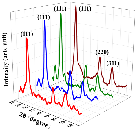
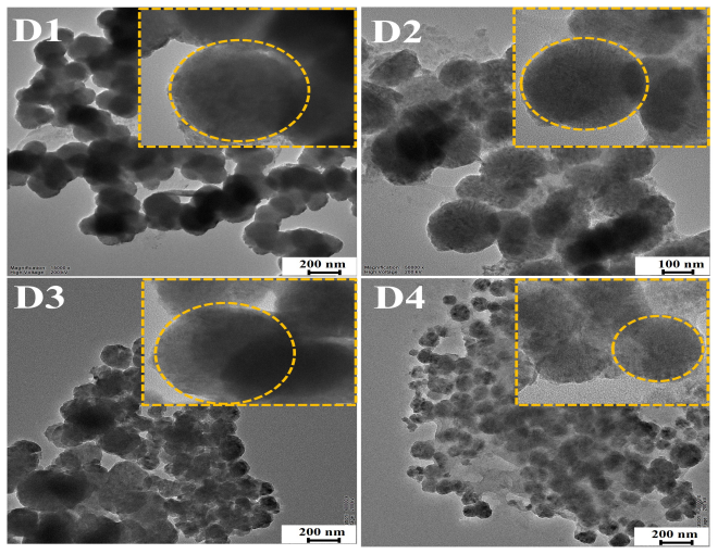
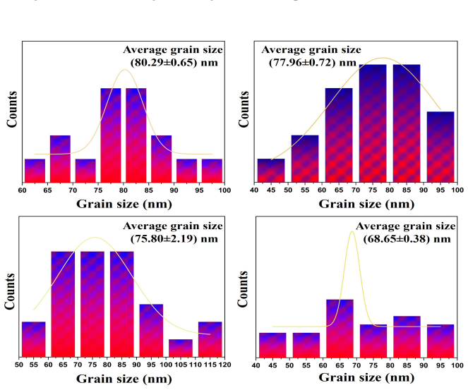
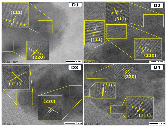
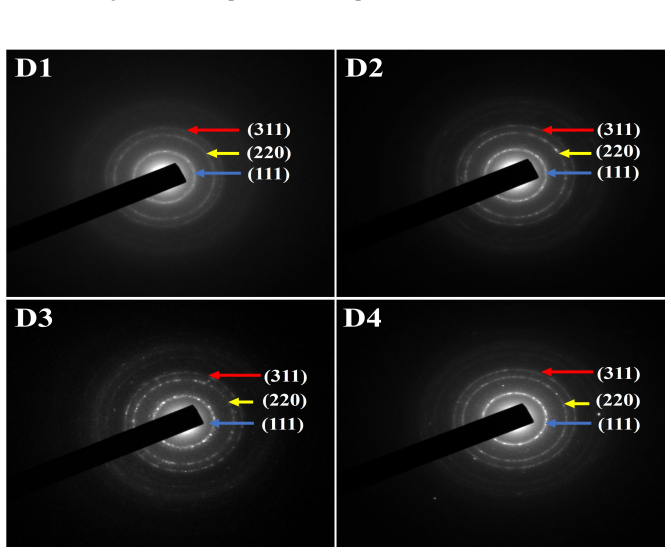
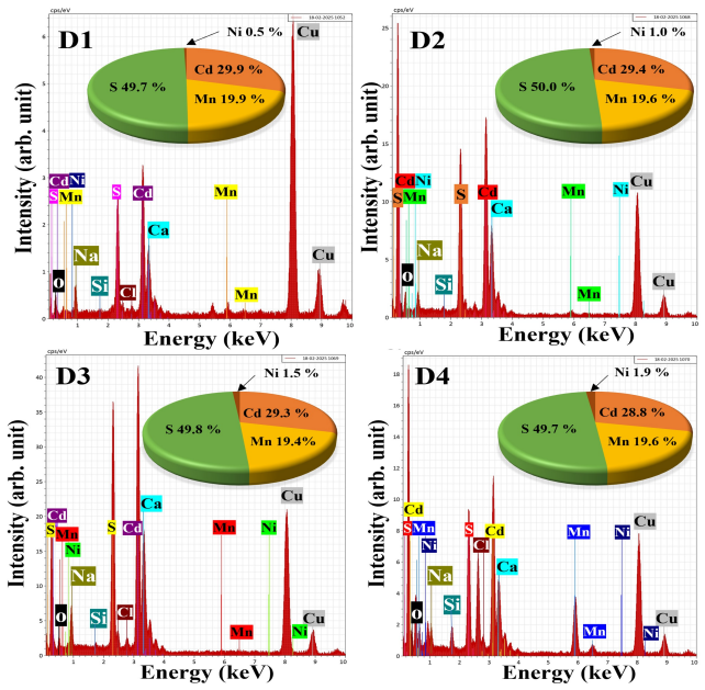
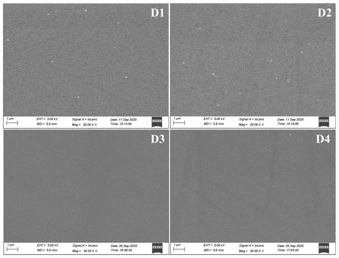
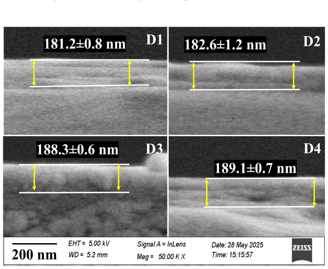
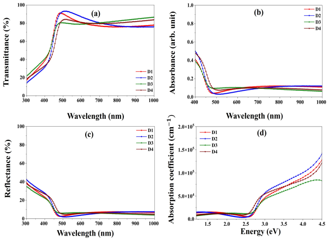
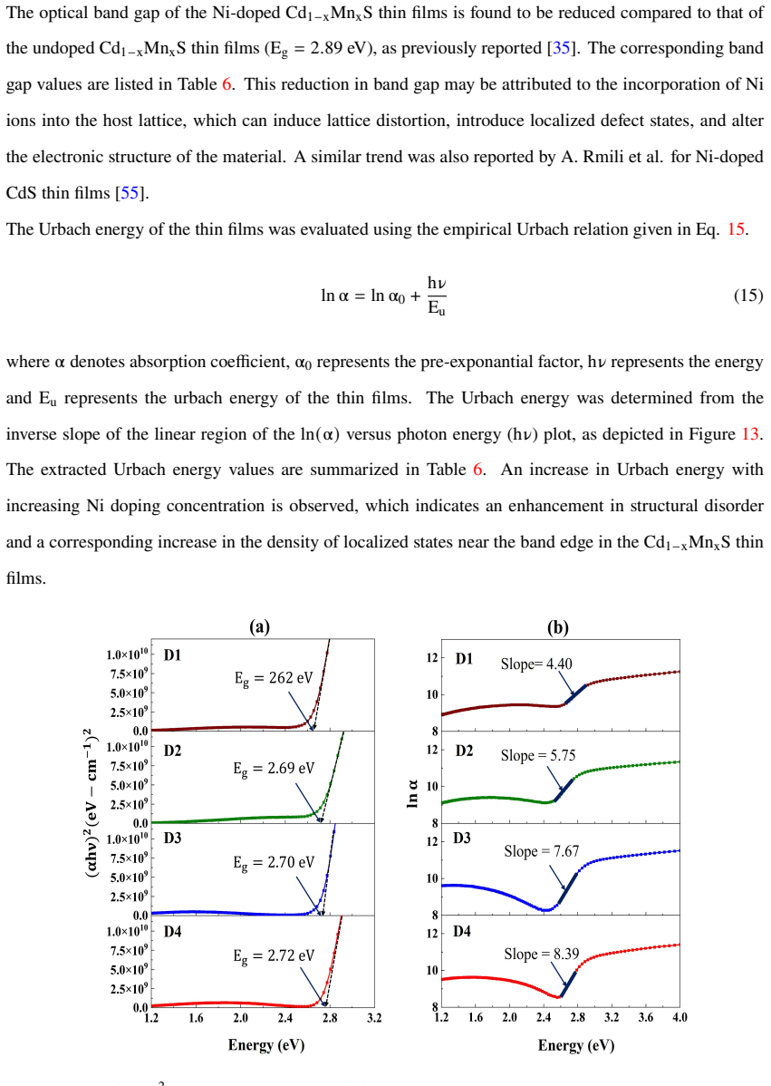
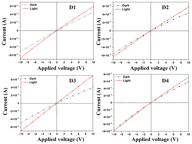
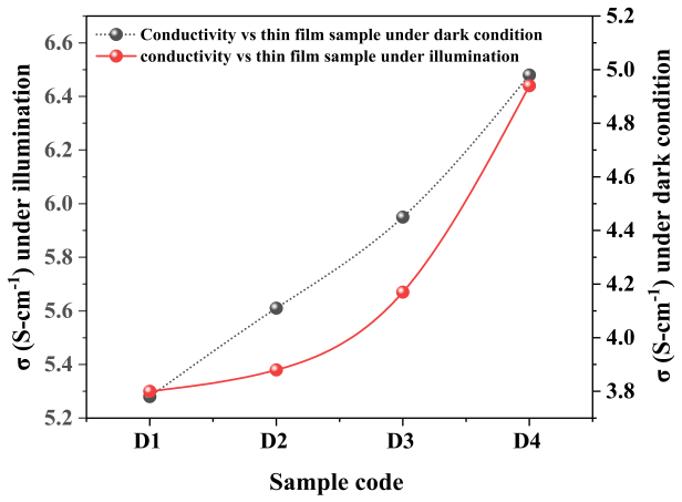
Ni-doped Cd1-xMnxS (x=0.4) thin films were prepared by chemical bath deposition. As Ni content increases from 1 to 4 percent, the cubic zinc-blende structure persists while crystallinity improves, microstrain and dislocation density fall, grain size grows, optical transmittance stays high at 75-90 percent across the visible and near-infrared, the band gap drops from 2.72 to 2.62 eV, and current-voltage characteristics show higher conductivity that rises further under illumination.
What carries the argument
Ni incorporation into the Cd1-xMnxS lattice through ionic-size mismatch and sp-d exchange interactions, which alters lattice strain, defect density, and electronic band structure.
If this is right
- Higher Ni levels steadily reduce the optical band gap while preserving high visible-NIR transmittance.
- Electrical conductivity increases and the films exhibit clear photoconducting response under light.
- Grain size grows and films remain uniform, dense, and crack-free with thickness near 185 nm.
- Reduced microstrain and dislocation density accompany the crystallinity gains.
- The tuned properties support use as window layers in thin-film solar cells and related optoelectronic devices.
Where Pith is reading between the lines
- The same Ni-doping route could be tested on other II-VI ternary films to achieve comparable band-gap and conductivity adjustments.
- Building complete solar-cell stacks with these doped films as the window layer would directly check whether the property changes raise device efficiency.
- Because the chemical bath method is low-cost and scalable, the doping strategy might enable large-area deposition of optimized window layers without vacuum equipment.
- Lower dislocation density could imply longer carrier diffusion lengths, a point worth measuring in future transport studies.
Load-bearing premise
The measured gains in crystallinity, transmittance, band gap, and conductivity arise from nickel atoms entering the lattice rather than from uncontrolled differences in deposition or measurement conditions.
What would settle it
Growing and characterizing undoped Cd1-xMnxS films under exactly the same bath conditions and showing identical rises in grain size, transmittance, and conductivity would falsify the claim that Ni doping produces the observed changes.
Figures
read the original abstract
Ni-doped Cd1-xMnxS (x=0.4) thin films were prepared via a cost-effective chemical bath deposition (CBD) method to investigate their suitability for optoelectronic applications. Incorporation of a secondary transition metal such as Ni is expected to influence lattice strain, defect density, and electronic structure through ionic size effects and sp-d exchange interactions, thereby providing an additional degree of freedom for tuning the properties of Cd1-xMnxS-based ternary systems. X-ray diffraction (XRD) analysis confirmed the cubic zinc blende structure of the Cd1-xMnxS crystal, which was further corroborated by high-resolution transmission electron microscopy (HRTEM). Crystallinity increases where as microstrain and dislocation density found to be decreases as the doping concentration of Ni increases. Field emission scanning electron microscopy (FESEM) analysis revealed uniform, dense, and crack-free films with grain size increasing as a function of Ni content, and the FESEM cross-sectional images indicated a nearly constant thickness in the range of 181.2-189.1 nm. The films exhibited high optical transmittance (75-90%) in the visible and near-infrared (NIR) regions. The optical band gap decreases from 2.72 to 2.62 eV as the Ni concentration increases from 1% to 4%. Current-voltage (I-V) measurements revealed enhanced electrical conductivity, which further increased under illumination, confirming the photoconducting nature of the films. These results demonstrate that Ni doping effectively tunes the properties of Cd1-xMnxS thin films, highlighting their potential as efficient window layer materials for thin-film solar cells and related optoelectronic devices.
Editorial analysis
A structured set of objections, weighed in public.
Referee Report
Summary. The manuscript describes the chemical bath deposition of Ni-doped Cd_{0.6}Mn_{0.4}S thin films (Ni concentrations 1–4%) and reports that increasing Ni content improves crystallinity, reduces microstrain and dislocation density, increases grain size, maintains high optical transmittance (75–90%), decreases the optical band gap from 2.72 to 2.62 eV, and enhances electrical conductivity (further under illumination). The authors conclude that Ni doping effectively tunes these properties, making the films suitable as window layers for thin-film solar cells.
Significance. If the observed trends can be unambiguously attributed to Ni incorporation, the work provides a useful experimental dataset on dual-transition-metal doping in CdS-based ternary films, with consistent results across XRD, HRTEM, FESEM, optical, and I-V measurements and nearly constant film thickness (181–189 nm). This could support materials optimization for optoelectronics, though the absence of error bars and statistical analysis reduces quantitative strength.
major comments (1)
- [Experimental section] Experimental section: The sample-preparation description does not explicitly state that Cd, Mn, and S precursor concentrations, bath pH, temperature, and deposition time were held strictly constant while only the Ni precursor concentration was varied. Although FESEM cross-sections show thickness limited to 181.2–189.1 nm, without this control the central claim that trends in crystallinity, band gap (2.72→2.62 eV), transmittance, and conductivity arise from Ni doping (via ionic-size and sp-d effects) cannot be isolated from possible changes in solution chemistry or nucleation kinetics.
minor comments (2)
- [Abstract and Results] Abstract and Results: No error bars, standard deviations, or replicate measurements are reported for XRD-derived parameters, band-gap values, or I-V data, weakening the ability to judge the statistical significance of the reported trends.
- [Throughout] Figure captions and text: Minor grammatical issues (e.g., “increases where as”) and occasional undefined abbreviations should be corrected for clarity.
Simulated Author's Rebuttal
We thank the referee for the constructive comments on our manuscript. The single major comment concerns the need for explicit clarification in the Experimental section regarding constant precursor concentrations and deposition parameters. We address this below and have revised the manuscript accordingly to strengthen the attribution of observed trends to Ni doping.
read point-by-point responses
-
Referee: [Experimental section] Experimental section: The sample-preparation description does not explicitly state that Cd, Mn, and S precursor concentrations, bath pH, temperature, and deposition time were held strictly constant while only the Ni precursor concentration was varied. Although FESEM cross-sections show thickness limited to 181.2–189.1 nm, without this control the central claim that trends in crystallinity, band gap (2.72→2.62 eV), transmittance, and conductivity arise from Ni doping (via ionic-size and sp-d effects) cannot be isolated from possible changes in solution chemistry or nucleation kinetics.
Authors: We agree that the Experimental section should explicitly confirm the controlled variables. In the revised manuscript, we have added the following statement: 'The concentrations of Cd, Mn, and S precursors, along with bath pH (maintained at 10.5), temperature (80°C), and deposition time (45 min), were held strictly constant while only the Ni precursor concentration was varied from 1% to 4%.' This ensures isolation of Ni-doping effects. The nearly constant film thickness (181.2–189.1 nm) from FESEM cross-sections, combined with consistent XRD, HRTEM, optical, and I-V trends, supports that solution chemistry and nucleation kinetics remained unchanged. These revisions directly address the concern and reinforce the role of ionic-size and sp-d exchange interactions in tuning the properties. revision: yes
Circularity Check
No circularity: purely experimental characterization with no derivations or models
full rationale
The paper is an experimental materials science study using chemical bath deposition to prepare Ni-doped Cd1-xMnxS thin films followed by direct characterization via XRD, HRTEM, FESEM, optical transmittance, band gap extraction, and I-V measurements. No equations, theoretical derivations, predictions, or first-principles calculations are present. All reported trends (crystallinity increase, band gap decrease from 2.72 to 2.62 eV, conductivity enhancement) are observational outcomes of measurements, not results derived from fitted parameters or self-referential definitions. No self-citations, ansatzes, or uniqueness theorems are invoked in a load-bearing way. The central claim that Ni doping tunes properties rests on experimental attribution rather than any closed logical loop. This matches the default expectation of no significant circularity for non-theoretical papers.
Axiom & Free-Parameter Ledger
Reference graph
Works this paper leans on
-
[1]
K. Sivaperuman, A. Thomas, R. Thangavel, L. Thirumalaisamy, S. Palanivel, S. Pitchaimuthu, N. Ahsan, and Y. Okada, “Binary and ternary metal oxide semiconductor thin films for effective gas sensingapplications: Acomprehensivereviewandfutureprospects,”ProgressinMaterialsScience, vol. 142, p. 101222, 2024
work page 2024
-
[2]
G. Gayathri, M. Rengasamy, and R. Thiruneelakanadan, “Fabrication, structural, optical, electrical propertiesofternaryfenis2thinfilmsanditsapplicationsinphotocatalyticdyedegradation,”Journal of Materials Science: Materials in Electronics, vol. 36, no. 7, p. 412, 2025
work page 2025
-
[3]
Introduction and fundamentals of chalcogenides and chalcogenides-based nanomate- rials,
M. M. Khan, “Introduction and fundamentals of chalcogenides and chalcogenides-based nanomate- rials,” inChalcogenide-based nanomaterials as photocatalysts, pp. 1–6, Elsevier, 2021
work page 2021
-
[4]
L. Li, P. C. Wu, X. S. Fang, T. Y. Zhai, L. Dai, M. Y. Liao, Y. Koide, H. Q. Wang, Y. Bando, andD.Golberg,“Single-crystallinecdsnanobeltsforexcellentfield-emittersandultrahighquantum- efficiency photodetectors,”Advanced Materials, vol. 22, no. 29, pp. 3161–3165, 2010
work page 2010
-
[5]
Sensing properties of cds-doped tin oxide thick film gas sensor,
L. Yadava, R. Verma, and R. Dwivedi, “Sensing properties of cds-doped tin oxide thick film gas sensor,”Sensors and Actuators B: Chemical, vol. 144, no. 1, pp. 37–42, 2010
work page 2010
-
[6]
High efficiency solar cells with cds window layers,
T. Coutts, “High efficiency solar cells with cds window layers,”Thin Solid Films, vol. 90, no. 4, pp. 451–460, 1982
work page 1982
-
[7]
Synthesis and characterization ofcds/pvananocompositethinfilmsfromacomplexingagentfreesystem,
D. Saikia, P. Saikia, P. Gogoi, M. Das, P. Sengupta, and M. Shelke, “Synthesis and characterization ofcds/pvananocompositethinfilmsfromacomplexingagentfreesystem,”MaterialsChemistryand Physics, vol. 131, no. 1-2, pp. 223–229, 2011
work page 2011
-
[8]
J.Bora,A.Borthakur,G.Arandhara,andP.Saikia,“Effectofagdopingontheopticalandstructural properties of cds/polyvinyl alcohol thin films by thermolysis process,”Thin Solid Films, vol. 734, p. 138847, 2021
work page 2021
-
[9]
P. Borah and P. K. Saikia, “Effect of cu doping on chemically deposited cd1- xznxs thin films: Syn- thesis,structural,morphological,optical,andelectricalinvestigationsforphotovoltaicapplications,” Journal of The Electrochemical Society, vol. 172, no. 12, p. 122503, 2025. 33
work page 2025
-
[10]
Recycled polycrystalline cds film electrodes with enhanced photo-electrochemical characteristics,
A. Zyoud, S. Al-Yamani, H. Bsharat, M. H. Helal, H. Kwon, D. Park, and H. S. Hilal, “Recycled polycrystalline cds film electrodes with enhanced photo-electrochemical characteristics,”Materials Science in Semiconductor Processing, vol. 74, pp. 277–283, 2018
work page 2018
-
[11]
A. Hannachi, A. Segura, and H. Maghraoui-Meherzi, “Growth of manganese sulfide (𝛼-mns) thin films by thermal vacuum evaporation: Structural, morphological and optical properties,”Materials Chemistry and Physics, vol. 181, pp. 326–332, 2016
work page 2016
-
[12]
E.Shokr,H.Mohamed,A.Ismail,M.Hasaneen,andH.Ali,“Opticalandelectricalpropertiesofthin films of mns/metal/mns for photocatalysis and gas sensing applications,”Optik, vol. 296, p. 171549, 2024
work page 2024
-
[13]
C. Ulutas, E. Guneri, F. Kirmizigul, G. Altindemir, F. Gode, and C. Gumus, “𝛾-mns thin films prepared by chemical bath deposition: Effect of bath temperature on their physical properties,” Materials Chemistry and Physics, vol. 138, no. 2-3, pp. 817–822, 2013
work page 2013
-
[14]
Growth of cdmns films by pulsed laser evaporation,
D.-S. Chuu, Y.-C. Chang, and C.-Y. Hsieh, “Growth of cdmns films by pulsed laser evaporation,” Thin Solid Films, vol. 304, no. 1-2, pp. 28–35, 1997
work page 1997
-
[15]
T. Veeramanikandasamy, K. Rajendran, K. Sambath, and P. Rameshbabu, “Effect of cu-doping on optical, electrical and magnetic properties of chemically synthesized mns nanocrystals,”Materials Chemistry and Physics, vol. 171, pp. 328–335, 2016
work page 2016
-
[16]
Structural,opticalandmagneticproperties ofbaandnidopedcdsthinfilmspreparedbyspraypyrolysismethod,
R.Murugesan,S.Sivakumar,P.Anandan,andM.Haris,“Structural,opticalandmagneticproperties ofbaandnidopedcdsthinfilmspreparedbyspraypyrolysismethod,”JournalofMaterialsScience: Materials in Electronics, vol. 28, no. 17, pp. 12432–12439, 2017
work page 2017
-
[17]
Structural,opticalandmagneticpropertiesofcdzns andni: Cdznsnanoparticles,
S.Horoz,M.Akyol,A.Ekicibil,andÖ.Sahin,“Structural,opticalandmagneticpropertiesofcdzns andni: Cdznsnanoparticles,”JournalofMaterialsScience: MaterialsinElectronics,vol.28,no.23, pp. 18193–18199, 2017
work page 2017
-
[18]
N. Naveenkumar, A. Abhishek, P. Umadevi, B. Neppolian, S. Mukaddar, T. S. Girisun, V. Ramesh, et al., “Improved photovoltaic efficiency and nonlinear optical response in ni-doped bi2o3 nanorod- based photoanodes for dye-sensitized solar cells,”Ceramics International, 2025
work page 2025
-
[19]
M. Y. Ali, M. Khan, A. T. Karim, M. M. Rahman, and M. Kamruzzaman, “Effect of ni doping on structure, morphology and opto-transport properties of spray pyrolised zno nano-fiber,”Heliyon, vol. 6, no. 3, 2020. 34
work page 2020
-
[20]
I. Yahia, I. El Radaf, A. Salem, and G. Sakr, “Chemically deposited ni-doped cds nanostructured thin films: optical analysis and current-voltage characteristics,”Journal of Alloys and Compounds, vol. 776, pp. 1056–1062, 2019
work page 2019
-
[21]
R. Luo, B. Liu, X. Yang, Z. Bao, B. Li, J. Zhang, W. Li, L. Wu, and L. Feng, “The large-area cdte thin film for cds/cdte solar cell prepared by physical vapor deposition in medium pressure,”Applied Surface Science, vol. 360, pp. 744–748, 2016
work page 2016
-
[22]
Reviewofnanostructuredniothinfilmdepositionusing thespraypyrolysistechnique,
K.Ukoba,A.Eloka-Eboka,andF.Inambao,“Reviewofnanostructuredniothinfilmdepositionusing thespraypyrolysistechnique,”RenewableandSustainableEnergyReviews,vol.82,pp.2900–2915, 2018
work page 2018
-
[23]
Recent advances in the growth and characterizations of silar-deposited thin films,
H. Soonmin, “Recent advances in the growth and characterizations of silar-deposited thin films,” Applied Sciences, vol. 12, no. 16, p. 8184, 2022
work page 2022
-
[24]
Electrical and optical properties of czts thin films prepared by silar method,
J. Henry, K. Mohanraj, and G. Sivakumar, “Electrical and optical properties of czts thin films prepared by silar method,”Journal of Asian Ceramic Societies, vol. 4, no. 1, pp. 81–84, 2016
work page 2016
-
[25]
Metal-organic chemical vapor deposition of aluminum scandium nitride,
S.Leone, J.Ligl, C.Manz, L.Kirste, T.Fuchs, H.Menner, M.Prescher, J.Wiegert, A.Žukauskait˙e, R. Quay,et al., “Metal-organic chemical vapor deposition of aluminum scandium nitride,”physica status solidi (RRL)–Rapid Research Letters, vol. 14, no. 1, p. 1900535, 2020
work page 2020
-
[26]
A. F. Abdulrahman, S. M. Ahmed, N. M. Ahmed, and M. A. Almessiere, “Enhancement of zno nanorodspropertiesusingmodifiedchemicalbathdepositionmethod: effectofprecursorconcentra- tion,”Crystals, vol. 10, no. 5, p. 386, 2020
work page 2020
-
[27]
H. S. Pathok, A. K. Das, and P. K. Saikia, “Effect of deposition time on the structural, optical, and electrical properties of chemically deposited cd1- xmnxs thin films,”Indian Journal of Physics, pp. 1–16, 2026
work page 2026
-
[28]
Dip-coating for fibrous materials: mechanism, methods and applications,
X. Tang and X. Yan, “Dip-coating for fibrous materials: mechanism, methods and applications,” Journal of Sol-Gel Science and Technology, vol. 81, no. 2, pp. 378–404, 2017
work page 2017
-
[29]
Low-temperatureacetonegassensingusingtailored zno/cu2oheterojunctionthinfilmsasgas-sensingelement,
K.Sonowal,A.T.T.Mostako,andP.K.Saikia,“Low-temperatureacetonegassensingusingtailored zno/cu2oheterojunctionthinfilmsasgas-sensingelement,”JournalofElectronicMaterials,vol.55, no. 1, pp. 220–232, 2026. 35
work page 2026
-
[30]
Shortreviewonchemicalbathdepositionofthinfilmandcharacterization,
D.MugleandG.Jadhav,“Shortreviewonchemicalbathdepositionofthinfilmandcharacterization,” inAIP Conference Proceedings, vol. 1728, p. 020597, AIP Publishing LLC, 2016
work page 2016
-
[31]
Z. M. Kakhaki, A. Youzbashi, P. Sangpour, N. Naderi, and Y. Orooji, “Influence of cd salt concen- tration on the photoconductivity of cds thin films prepared by chemical bath technique,”Materials Science in Semiconductor Processing, vol. 148, p. 106773, 2022
work page 2022
-
[32]
H. A. Hasan, N. A. Hussein Al-Assady, H. A. Badran, R. K. Alfahed, and K. I. Ajeel, “Effects of temperature on structural and linear/nonlinear optical properties of cds nanoparticles film deposited by chemical reaction method,”Optical and Quantum Electronics, vol. 55, no. 6, p. 555, 2023
work page 2023
-
[33]
M.N.Murthy,C.Sreelatha,G.Ravinder,andS.Anusha,“Theeffectofsolutionphonthestructural, surfacemorphological,andopticalcharacteristicsofznothinfilmssynthesizedbythechemicalbath deposition technique,”Materials Today: Proceedings, vol. 54, pp. 602–607, 2022
work page 2022
-
[34]
S.Adhyapak,M.Boruah,H.S.Pathok,A.K.Das,andP.K.Saikia,“Chemicallydepositednanocrys- tallineznmgsthinfilm: Theimpactofdepositiontimeonitsstructuralandopticalproperties,”Physica B: Condensed Matter, vol. 694, p. 416443, 2024
work page 2024
-
[35]
H. S. Pathok, A. K. Das, M. Boruah, S. Adhyapak, and P. K. Saikia, “Effect of mn concentration on the structural, morphological, optical, and electrical properties of cd1-xmnxs thin films,”Thin Solid Films, p. 140828, 2025
work page 2025
-
[36]
S. Liu, Y. Li, Q. Liu, J. Tao, and X. Zheng, “Plasma-enhanced atomic layer deposition of crystalline gan thin films on quartz substrates with sharp interfaces,”Journal of Vacuum Science & Technology A, vol. 41, no. 5, 2023
work page 2023
-
[37]
A. Hannachi, S. Hammami, N. Raouafi, and H. Maghraoui-Meherzi, “Preparation of manganese sulfide(mns)thinfilmsbychemicalbathdeposition: Applicationoftheexperimentaldesignmethod- ology,”Journal of Alloys and Compounds, vol. 663, pp. 507–515, 2016
work page 2016
-
[38]
Fabrication and characterization of chemically deposited copper–manganese sulfide thin films,
S. Salem, N. M. Deraz, and H. A. Saleh, “Fabrication and characterization of chemically deposited copper–manganese sulfide thin films,”Applied Physics A, vol. 126, no. 9, p. 700, 2020
work page 2020
-
[39]
H.S.Pathok,A.T.T.Mostako,andP.K.Saikia,“Comprehensiveanalysisofthestructural,morpho- logical, optical, and electrical characteristics of undoped and cobalt-doped cd1-xmnxs thin films,” Journal of Solid State Chemistry, p. 125926, 2026. 36
work page 2026
-
[40]
Cds nanofilms: effect of film thickness on morphology and optical band gap,
S. Kumar, S. Kumar, P. Sharma, V. Sharma, and S. Katyal, “Cds nanofilms: effect of film thickness on morphology and optical band gap,”Journal of Applied Physics, vol. 112, no. 12, 2012
work page 2012
-
[41]
K. C. Kumar and S. Kaleemulla, “Effect of ni incorporation on structural, optical and magnetic properties of electron beam evaporated zns thin films,”Journal of Physics and Chemistry of Solids, vol. 135, p. 109028, 2019
work page 2019
-
[42]
Influence of magnesium dopant on zns thin films by low-cost chemical bath deposition technique,
V. Ashith and S. N. Moger, “Influence of magnesium dopant on zns thin films by low-cost chemical bath deposition technique,”Optik, vol. 284, p. 170934, 2023
work page 2023
-
[43]
G. Arandhara and P. K. Saikia, “Silver insertion: Exploring the impact of ag doping on the optical andstructuralpropertiesofznsnanostructuredthinfilms,”PhysicaB:CondensedMatter,p.418252, 2026
work page 2026
-
[44]
A. Borgogoi and A. Mostako, “Controlled crystalline phase transformation mos2 thin films with 2d nano-flakes by unique vapour-plasma mixing technique,”Optical Materials, vol. 165, p. 117136, 2025
work page 2025
-
[45]
Multifunctional czts thin films: structural, optoelectrical, electrical and photovoltaic properties,
S. Fouad, I. El Radaf, P. Sharma, and M. El-Bana, “Multifunctional czts thin films: structural, optoelectrical, electrical and photovoltaic properties,”Journal of Alloys and Compounds, vol. 757, pp. 124–133, 2018
work page 2018
-
[46]
The annealing effect on microstructure and esr properties of (cu/ni) co-doped zno nanoparticles,
A. Guler, L. Arda, N. Dogan, C. Boyraz, and E. Ozugurlu, “The annealing effect on microstructure and esr properties of (cu/ni) co-doped zno nanoparticles,”Ceramics International, vol. 45, no. 2, pp. 1737–1745, 2019
work page 2019
-
[47]
Characterization of cds thin-film in high efficient cds/cdte solar cells,
M. Tsuji, T. Aramoto, H. Ohyama, T. Hibino, and K. Omura, “Characterization of cds thin-film in high efficient cds/cdte solar cells,”Japanese Journal of Applied Physics, vol. 39, no. 7R, p. 3902, 2000
work page 2000
-
[48]
Interrelation of micro-strain, energy band gap and pl intensity in ce doped zns quantum structures,
P.Kumari,K.P.Misra,S.Samanta,A.Rao,A.Bandyopadhyay,andS.Chattopadhyay,“Interrelation of micro-strain, energy band gap and pl intensity in ce doped zns quantum structures,”Journal of Luminescence, vol. 251, p. 119258, 2022
work page 2022
-
[49]
Stabilityandelectronicpropertiesofcd0.75mn0.25sandcd0.75mn0.25se in b3 phase,
A.RaniandR.Kumar,“Stabilityandelectronicpropertiesofcd0.75mn0.25sandcd0.75mn0.25se in b3 phase,”Applied Physics A, vol. 120, no. 2, pp. 775–784, 2015. 37
work page 2015
-
[50]
M. Boruah, S. Adhyapak, A. K. Das, H. S. Pathok, and P. K. Saikia, “Structural and optical characterizationofdepositiondurationvariedchemicallydepositednanostructuredznssethinfilms,” Journal of Materials Science: Materials in Electronics, vol. 36, no. 3, p. 181, 2025
work page 2025
-
[51]
N. S. Begum, H. Farveez Ahmed, and K. Gunashekar, “Effects of ni doping on photocatalytic activity of tio2 thin films prepared by liquid phase deposition technique,”Bulletin of Materials Science, vol. 31, no. 5, pp. 747–751, 2008
work page 2008
-
[52]
Effect of ni on thegrowthandphotoelectrochemicalpropertiesofznsthinfilms,
C.-M. Huang, L.-C. Chen, G.-T. Pan, T. C. Yang, W.-S. Chang, and K.-W. Cheng, “Effect of ni on thegrowthandphotoelectrochemicalpropertiesofznsthinfilms,”MaterialsChemistryandPhysics, vol. 117, no. 1, pp. 156–162, 2009
work page 2009
-
[53]
L. Gogoi, A. K. Das, S. Chaliha, and P. K. Saikia, “Investigation on the structural properties and correlationoftheopticalconstantsofcd1-xznxsthinfilmswithbathdepositiontemperature,”Chinese Journal of Physics, vol. 74, pp. 389–405, 2021
work page 2021
-
[54]
L. Gogoi, S. Chaliha, D. J. Borah, and P. Saikia, “Influence of cd content on structural and optical propertiesofchemicalbathdepositedcdxpb1-xsthinfilms,”BulletinofMaterialsScience,vol.44, no. 3, p. 225, 2021
work page 2021
-
[55]
A.Rmili,F.Ouachtari,A.Bouaoud,A.Louardi,T.Chtouki,B.Elidrissi,andH.Erguig,“Structural, optical and electrical properties of ni-doped cds thin films prepared by spray pyrolysis,”Journal of alloys and Compounds, vol. 557, pp. 53–59, 2013
work page 2013
-
[56]
Annealingtemperatureeffectonthestructural,opticalandelectricalpropertiesofznsthin films,
F.Göde,“Annealingtemperatureeffectonthestructural,opticalandelectricalpropertiesofznsthin films,”Physica B: Condensed Matter, vol. 406, no. 9, pp. 1653–1659, 2011
work page 2011
-
[57]
The structural, electrical and optical properties of cds thin films as a function of ph,
A. Kariper, E. Güneri, F. Göde, C. Gümüş, and T. Özpozan, “The structural, electrical and optical properties of cds thin films as a function of ph,”Materials Chemistry and Physics, vol. 129, no. 1-2, pp. 183–188, 2011
work page 2011
-
[58]
Adjusting the relation between the imaginary part of the dielectric constant and the wave- length,
K. Aly, “Adjusting the relation between the imaginary part of the dielectric constant and the wave- length,”Physica B: Condensed Matter, vol. 655, p. 414723, 2023
work page 2023
-
[59]
C. Ulutas, O. Erken, M. Gunes, and C. Gumus, “The effects of substrate on the physical properties of gamma-mns thin films deposited by chemical bath deposition,”Physica B: Condensed Matter, vol. 588, p. 412175, 2020. 38
work page 2020
-
[60]
Anewdielectric hybrid complex for ambient temperature capacitive energy storage,
K.H.Alharbi,C.Ayari,W.Alharbi,A.A.Alotaibi,A.Othmani,andM.H.Mrad,“Anewdielectric hybrid complex for ambient temperature capacitive energy storage,”Journal of Energy Storage, vol. 70, p. 107984, 2023
work page 2023
-
[61]
A. H. Ali, Z. Hassan, and A. Shuhaimi, “Enhancement of optical transmittance and electrical resistivity of post-annealed ito thin films rf sputtered on si,”Applied Surface Science, vol. 443, pp. 544–547, 2018
work page 2018
-
[62]
S.AlKuhaimi,“Influenceofpreparationtechniqueonthestructural,opticalandelectricalproperties of polycrystalline cds films,”Vacuum, vol. 51, no. 3, pp. 349–355, 1998
work page 1998
-
[63]
Physicalpropertiesofchemicallyspraydepositednanocrystallinemanganesesulfide (mns)thinfilms,
S.G.Ibrahim,“Physicalpropertiesofchemicallyspraydepositednanocrystallinemanganesesulfide (mns)thinfilms,”JournalofMaterialsScience: MaterialsinElectronics,vol.32,no.1,pp.543–550, 2021
work page 2021
-
[64]
Analysis of chemically deposited mns thin films,
F. Ezema, “Analysis of chemically deposited mns thin films,” 2007
work page 2007
-
[65]
A. K. Das, L. Gogoi, J. Bora, I. Ali, M. Boruah, P. Borah, S. Adhyapak, H. S. Pathok, and P. K. Saikia, “Insight into deposition duration-varied crystallinity, optical parameters, morphology and electrical properties of solution-processed nanostructured cdsse thin films,”Optical Materials, vol. 156, p. 116017, 2024
work page 2024
-
[66]
M. Boruah, S. Adhyapak, A. K. Das, H. S. Pathok, A. Mostako, and P. K. Saikia, “Low-temperature synthesisandcharacterizationofchemicallydepositedph-variednanocrystallineznssethinfilmsfor application in photovoltaics,”Optical Materials, vol. 159, p. 116621, 2025. 39
work page 2025
discussion (0)
Sign in with ORCID, Apple, or X to comment. Anyone can read and Pith papers without signing in.