A simple method to fabricate Josephson junctions
Pith reviewed 2026-05-07 17:01 UTC · model grok-4.3
The pith
Photolithography and argon etching produce tunable, stable Josephson junctions for quantum circuits.
A machine-rendered reading of the paper's core claim, the machinery that carries it, and where it could break.
Core claim
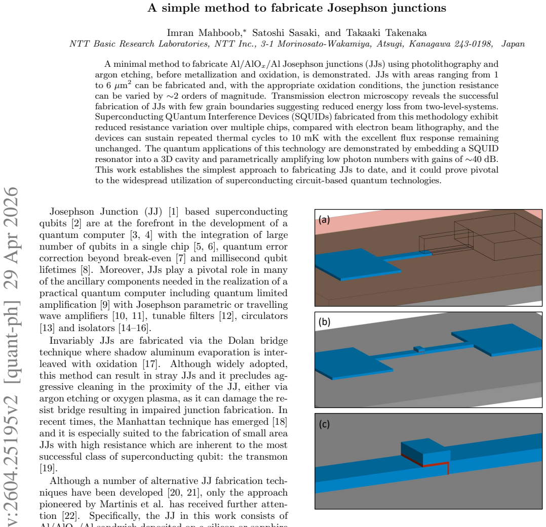
Josephson junctions with areas from 1 to 6 square micrometers are formed by first patterning the desired geometry with photolithography and argon etching, followed by aluminum metallization and controlled oxidation. Transmission electron microscopy images reveal junctions with minimal grain boundaries. SQUIDs built from these junctions display reduced resistance variation across chips and retain their flux response after repeated thermal cycling to 10 millikelvin. Embedding one such SQUID resonator in a 3D cavity allows parametric amplification of low photon numbers with gains of approximately 40 dB.
What carries the argument
The photolithography-plus-argon-etch sequence that patterns the junction area prior to metal deposition and oxidation.
Load-bearing premise
That the few grain boundaries seen in TEM directly reduce two-level-system loss and that the low chip-to-chip resistance variation and thermal-cycle stability come from the photolithography-and-etch steps rather than from other process details or from selecting only the best devices.
What would settle it
Fabricating multiple SQUIDs with the described method and measuring either large resistance spreads between chips or clear degradation in flux response after several cool-downs to 10 millikelvin would falsify the stability and uniformity claims.
Figures


read the original abstract
A minimal method to fabricate Al/AlO$_x$/Al Josephson junctions (JJs) using photolithography and argon etching, before metallization and oxidation, is demonstrated. JJs with areas ranging from 1 to 6 $\mu$m$^2$ can be fabricated and, with the appropriate oxidation conditions, the junction resistance can be varied by $\sim$2 orders of magnitude. Transmission electron microscopy reveals the successful fabrication of JJs with few grain boundaries suggesting reduced energy loss from two-level-systems. Superconducting QUantum Interference Devices (SQUIDs) fabricated from this methodology exhibit reduced resistance variation over multiple chips, compared with electron beam lithography, and the devices can sustain repeated thermal cycles to 10 mK with the excellent flux response remaining unchanged. The quantum applications of this technology are demonstrated by embedding a SQUID resonator into a 3D cavity and parametrically amplifying low photon numbers with gains of $\sim$40 dB. This work establishes the simplest approach to fabricating JJs to date, and it could prove pivotal to the widespread utilization of superconducting circuit-based quantum technologies.
Editorial analysis
A structured set of objections, weighed in public.
Referee Report
Summary. The manuscript presents a minimal fabrication process for Al/AlOx/Al Josephson junctions that relies on photolithography and argon etching prior to metallization and oxidation. Junctions with areas of 1–6 μm² are realized, with resistance tunable over approximately two orders of magnitude via oxidation conditions. TEM imaging indicates junctions with few grain boundaries. SQUIDs fabricated by this route show lower resistance variation across chips than those made by electron-beam lithography and remain stable through repeated thermal cycling to 10 mK. Functionality is demonstrated by embedding a SQUID resonator in a 3D cavity and achieving ~40 dB parametric gain at low photon numbers.
Significance. If the reported performance metrics and stability hold under quantitative scrutiny, the method would lower the equipment barrier for producing functional Josephson junctions, potentially accelerating prototyping of superconducting quantum circuits. The explicit demonstration of 40 dB parametric amplification supplies concrete evidence that the junctions support coherent microwave operation.
major comments (3)
- [Abstract / SQUID results] Abstract and SQUID-results paragraph: the claim of 'reduced resistance variation over multiple chips' is presented without numerical values, standard deviations, histograms, or the number of devices measured; without these data the comparison to electron-beam lithography cannot be evaluated quantitatively.
- [TEM analysis] TEM and loss discussion: the inference that 'few grain boundaries suggest reduced energy loss from two-level-systems' is not accompanied by direct measurements of loss tangent, 1/f noise spectra, or qubit T1/T2 times; the causal link therefore remains untested.
- [Quantum applications section] Parametric-amplifier demonstration: while 40 dB gain is reported, no side-by-side comparison with junctions fabricated by conventional methods on the same substrate is provided, so the contribution of the photolithography-plus-etch sequence to the observed performance cannot be isolated.
minor comments (2)
- [Methods] Process parameters (etch time, power, oxidation pressure and time) are stated only qualitatively; explicit numerical values and tolerances would improve reproducibility.
- [Results] The manuscript does not report device yield or the fraction of working junctions per wafer; inclusion of these statistics would strengthen the practicality claim.
Simulated Author's Rebuttal
We thank the referee for their thorough review and constructive feedback. We address each major comment below and outline the revisions we will make to strengthen the manuscript.
read point-by-point responses
-
Referee: [Abstract / SQUID results] Abstract and SQUID-results paragraph: the claim of 'reduced resistance variation over multiple chips' is presented without numerical values, standard deviations, histograms, or the number of devices measured; without these data the comparison to electron-beam lithography cannot be evaluated quantitatively.
Authors: We agree that quantitative support is required to substantiate the claim of reduced variation. In the revised manuscript we will add a dedicated figure (or table) showing the measured normal-state resistances for SQUIDs fabricated on multiple chips, including the number of devices tested (approximately 15 devices per chip across five chips), the standard deviation, and a direct comparison to devices fabricated by electron-beam lithography in our laboratory under otherwise identical conditions. This will allow a quantitative evaluation of the improvement. revision: yes
-
Referee: [TEM analysis] TEM and loss discussion: the inference that 'few grain boundaries suggest reduced energy loss from two-level-systems' is not accompanied by direct measurements of loss tangent, 1/f noise spectra, or qubit T1/T2 times; the causal link therefore remains untested.
Authors: We accept that the manuscript does not contain direct loss or coherence measurements. The statement draws on prior literature that correlates grain boundaries in aluminum films with two-level-system defects. To prevent over-interpretation we will revise the wording to “few grain boundaries, which literature associates with potentially lower loss from two-level systems” and will add the relevant citations. Direct characterization of loss tangent or qubit lifetimes lies beyond the scope of the present fabrication-focused study and will be addressed in follow-on work. revision: partial
-
Referee: [Quantum applications section] Parametric-amplifier demonstration: while 40 dB gain is reported, no side-by-side comparison with junctions fabricated by conventional methods on the same substrate is provided, so the contribution of the photolithography-plus-etch sequence to the observed performance cannot be isolated.
Authors: We agree that a controlled side-by-side comparison on the same substrate would more cleanly isolate the effect of the fabrication sequence. The section’s purpose is to show that junctions produced by this minimal process can nevertheless support coherent, high-gain parametric amplification at low photon numbers. We will add a brief discussion noting that the achieved gain and stability are comparable to values reported in the literature for conventional processes, while emphasizing that the method removes the need for electron-beam lithography. Because a direct comparative experiment was not performed, we do not claim superiority on the basis of the amplifier data alone. revision: no
Circularity Check
No circularity: purely experimental fabrication and measurement claims
full rationale
The paper presents an experimental fabrication process for Josephson junctions using photolithography and argon etching, supported by direct TEM imaging, resistance measurements, SQUID flux response data, and a parametric amplifier demonstration. No mathematical derivations, fitted models, predictions from equations, or self-citations of uniqueness theorems appear in the provided text or abstract. All claims rest on observed outcomes from the described process rather than any reduction of results to inputs by construction. The absence of any derivation chain means no load-bearing steps can be identified as circular under the specified patterns.
Axiom & Free-Parameter Ledger
Reference graph
Works this paper leans on
-
[1]
A simple method to fabricate Josephson junctions
and isolators [14–16]. Invariably JJs are fabricated via the Dolan bridge technique where shadow aluminum evaporation is inter- leaved with oxidation [17]. Although widely adopted, this method can result in stray JJs and it precludes ag- gressive cleaning in the proximity of the JJ, either via argon etching or oxygen plasma, as it can damage the re- sist ...
work page internal anchor Pith review Pith/arXiv arXiv 2026
-
[2]
A. L. Solovjev and S. I. Bondarenko, Low Temp. Phys. 50, 921 (2024)
work page 2024
-
[3]
P. Krantz, , M. Kjaergaard, F. Yan, T. P. Orlando, S. Gustavsson, and W. D. Oliver, Appl. Phys. Rev. 6, 021318 (2019)
work page 2019
- [4]
- [5]
- [6]
- [7]
-
[8]
V. V. Sivak, A. Eickbusch, B. Royer, S. Singh, I. Tsiout- sios, S. Ganjam, A. Miano, B. L. Brock, A. Z. Ding, L. Frunzio, et al., Nature 616, 50 (2023)
work page 2023
-
[9]
M. P. Bland et al., Nature 647, 343 (2025)
work page 2025
-
[10]
Aumentado, IEEE Microwave magazine 21, 45 (2020)
J. Aumentado, IEEE Microwave magazine 21, 45 (2020)
work page 2020
-
[11]
M. A. Castellanos-Beltran and K. W. Lehnert, Appl. Phys. Lett. 91, 083509 (2007)
work page 2007
-
[12]
C. Macklin, K. O’Brien, D. Hover, M. E. Schwartz, V. Bolkhovsky, X. Zhang, W. D. Oliver, and I. Siddiqi, Science 350, 307 (2015)
work page 2015
-
[13]
S. Kono, K. Koshino, D. Lachance-Quirion, A. F. van Loo, Y. Tabuchi, A. Noguchi, and Y. Nakamura, Nature Commun. 11, 3683 (2020)
work page 2020
-
[14]
B. J. Chapman, E. I. Rosenthal, J. Kerckhoff, B. A. Moores, L. R. Vale, J. Mates, G. C. Hilton, K. Lalu- miere, A. Blais, and K. W. Lehnert, Phys. Rev. X 7, 041043 (2019)
work page 2019
-
[15]
B. Abdo, N. T. Bronn, O. Jinka, S. Olivadese, A. D. Corcoles, V. P. Adiga, M. Brink, R. E. Lake, X. Wu, D. P. Pappas, et al., Nature Commun. 10, 3154 (2019)
work page 2019
- [16]
- [17]
-
[18]
G. J. Dolan, Appl. Phys. Lett. 31, 337 (1977)
work page 1977
- [19]
-
[20]
J. Koch, T. M. Yu, J. Gambetta, A. A. Houck, D. I. Schuster, J. Majer, A. Blais, M. H. Devoret, S. M. Girvin, and R. J. Schoelkopf, Phys. Rev. A 76, 042319 (2007)
work page 2007
- [21]
-
[22]
J. T. Monroe, D. Kowsari, K. Zheng, C. Gaikwad, J. Brewster, D. S. Wisbey, and K. W. Murch, Appl. Phys. Lett. 119, 062601 (2021)
work page 2021
- [23]
-
[24]
X. Wu, J. L. Long, H. S. Ku, R. E. Lake, M. Bal, and D. P. Pappas, Appl. Phys. Lett. 111, 032602 (2017)
work page 2017
- [25]
-
[26]
J. Braumuller, J. Cramer, S. Schlor, H. Rotzinger, L. Radtke, A. Lukashenko, P. Yang, S. T. Skacel, S. Probst, M. Marthaler, et al., Phys. Rev. B 91, 054523 (2021)
work page 2021
- [27]
-
[28]
N. Foroozani et al., Quantum Sci. Technol. 4, 025012 (2019)
work page 2019
-
[29]
J. V. Damme, S. Massar, R. Acharya, T. Ivanova, D. P. Lozano, Y. Canvel, M. Demarets, D. Vangoidsenhoven, Y. Hermans, J. G. Lai, et al., Nature 634, 74 (2024)
work page 2024
-
[30]
S. J. K. Lang, T. Mayer, J. Weber, C. Dhieb, Eisele, W. Lerch, Z. Luo, C. M. Guizan, E. Music, L. Sturm- Rogon, et al., Phys. Rev. Applied 24, 054052 (2025)
work page 2025
-
[31]
https://www.tok-pr.com/en/products/photoresist/ g-i-line.html
-
[32]
https://www.nanosystem-solutions.com/en/product/ maskless
-
[33]
https://www.kanto.co.jp/products/denshi/kinosei/ resist_strippers_developer/tmk_tma.html
- [34]
-
[35]
https://plassys.com/categories/MEB-Ebeam/ MEB550S
-
[36]
https://www.agasem.com/products-and-services/ semiconductors/microposit-remover-1165/
-
[37]
J. Biznarova, A. Osman, E. Rehnman, L. Chayanun, P. M. Christian Krizan, M. Rommel, C. Warren, P. Dels- ing, A. Yurgens, J. Bylander, et al., Npj Quantum Inf. 10, 78 (2024)
work page 2024
- [38]
-
[39]
T. Yamamoto, K. Inomata, M. Watanabe, K. Matsuba, T. Miyazaki, W. D. Oliver, Y. Nakamura, and J. S. Tsai, Appl. Phys. Lett. 93, 042510 (2008)
work page 2008
discussion (0)
Sign in with ORCID, Apple, or X to comment. Anyone can read and Pith papers without signing in.