Voltage-Regulated Photoluminescence Modulation in a 0D-2D Mixed Dimensional Heterostructure
Pith reviewed 2026-05-07 12:59 UTC · model grok-4.3
The pith
In a 0D-2D heterostructure, voltage bias produces photoluminescence oscillations by modulating an oscillatory photocurrent with periodic negative differential resistance from recurring charge accumulation.
A machine-rendered reading of the paper's core claim, the machinery that carries it, and where it could break.
Core claim
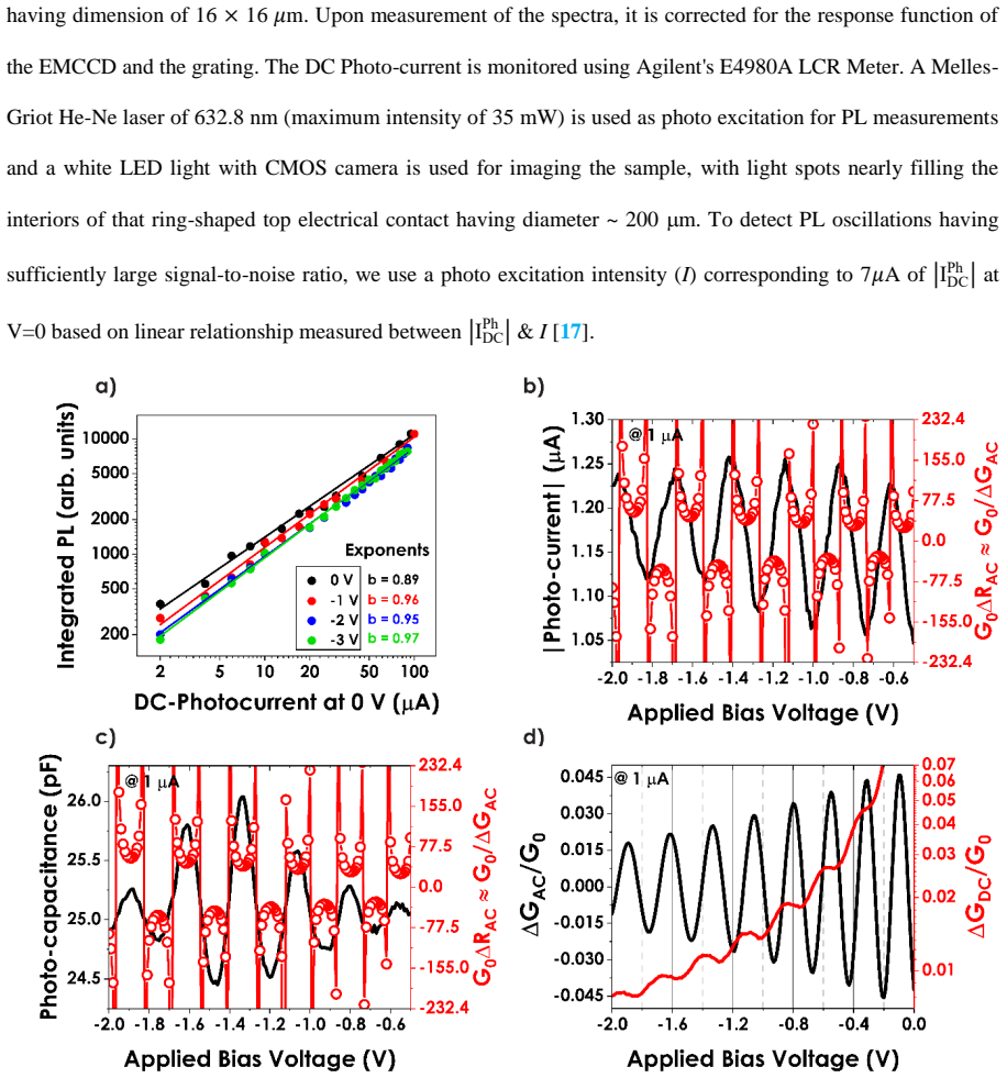
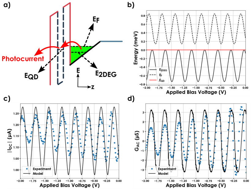
Bias-dependent oscillations in excitonic photoluminescence are observed in a mixed dimensional 0D-2D heterostructure. These oscillations arise from modulation by oscillatory DC photocurrent, which exhibits periodic negative differential resistance, indicating recurring charge accumulation within the heterostructure. The persistence of these oscillations across a macroscopic area of diameter around 200 microns suggests the presence of periodically correlated quantum phenomena over large length scales. Furthermore, bias dependent oscillations in the photo capacitance are observed, reflecting a periodic ordering and disordering of excitonic populations. Together, these observations point to a 1
What carries the argument
The modulation of excitonic photoluminescence by an oscillatory DC photocurrent that shows periodic negative differential resistance due to recurring charge accumulation, interpreted as arising from competition between coherent and incoherent electron tunneling.
If this is right
- Voltage can regulate photoluminescence output through control of the underlying photocurrent oscillations.
- Periodic ordering and disordering of excitons can be read out electrically via photo-capacitance oscillations.
- The competition between coherent and incoherent tunneling can be tuned by bias to produce coupled oscillatory responses in light emission, current, and capacitance.
- The macroscopic persistence opens a path to scalable exciton-based optoelectronic elements that exploit the observed tunneling competition.
- New device architectures become possible in which bias voltage directly programs oscillatory behavior in quantum optoelectronics.
Where Pith is reading between the lines
- Similar voltage-regulated oscillatory photoluminescence might be engineered in other low-dimensional heterostructures that support charge accumulation and tunneling.
- The large-scale correlation could be tested by fabricating devices with varying lateral sizes to determine the maximum distance over which the periodic behavior remains coherent.
- If the tunneling competition is the root cause, applying microwave or optical probes tuned to the oscillation frequency might reveal additional signatures of coherent versus incoherent processes.
- Device integration could explore whether the same bias control simultaneously modulates emission wavelength or coherence time in addition to intensity.
Load-bearing premise
The assumption that persistence of the oscillations over a 200-micron macroscopic area demonstrates periodically correlated quantum phenomena on large length scales and that the oscillations specifically result from modulation by the photocurrent's periodic negative differential resistance caused by charge accumulation.
What would settle it
Measuring no photoluminescence oscillations in regions where the DC photocurrent lacks periodic negative differential resistance, or finding that the oscillations appear only locally rather than uniformly across the full 200-micron area, would undermine the proposed mechanism and large-scale correlation.
Figures
read the original abstract
Bias dependent oscillations in excitonic photoluminescence are observed in a mixed dimensional 0D 2D heterostructure. These oscillations arise from modulation by oscillatory DC photocurrent, which exhibits periodic negative differential resistance, indicating recurring charge accumulation within the heterostructure. The persistence of these oscillations across a macroscopic area of diameter around 200 microns suggests the presence of periodically correlated quantum phenomena over large length scales. Furthermore, bias dependent oscillations in the photo capacitance are observed, reflecting a periodic ordering and disordering of excitonic populations. Together, these observations point to a direct competition between coherent and incoherent electron tunnelling processes. The coupled oscillatory behaviour of photoluminescence, photocurrent, and photo capacitance highlights new opportunities for exciton-based quantum optoelectronic devices.
Editorial analysis
A structured set of objections, weighed in public.
Referee Report
Summary. The manuscript reports bias-dependent oscillations in excitonic photoluminescence in a 0D-2D mixed-dimensional heterostructure. These are attributed to modulation by an oscillatory DC photocurrent that exhibits periodic negative differential resistance arising from recurring charge accumulation. Oscillations are also reported in photo-capacitance, interpreted as periodic ordering and disordering of excitonic populations. The persistence of the oscillations over a macroscopic area of ~200 μm is taken to indicate periodically correlated quantum phenomena on large length scales, with the overall behavior pointing to a direct competition between coherent and incoherent electron tunneling processes.
Significance. If the central interpretations are substantiated, the work would identify a new voltage-tunable oscillatory regime in hybrid 0D-2D systems that couples photoluminescence, photocurrent, and capacitance. This could open pathways for exciton-based optoelectronic devices exploiting large-scale correlations. The experimental observation of coupled oscillations is potentially interesting for mesoscopic transport studies, but its significance cannot be fully assessed without quantitative modeling and controls that distinguish the proposed tunneling mechanism from classical alternatives.
major comments (3)
- [Abstract / Results] Abstract and main text: The strongest claim—that the data demonstrate 'a direct competition between coherent and incoherent electron tunnelling processes'—is not supported by distinguishing measurements. No magnetic-field dependence, temperature scaling, or rate-equation modeling is presented to separate phase-coherent tunneling from incoherent hopping or from classical RC relaxation and trap-filling dynamics that can also generate periodic NDR.
- [Discussion] Discussion of large-scale correlations: The interpretation that persistence of oscillations across a ~200 μm diameter indicates 'periodically correlated quantum phenomena over large length scales' rests on an untested assumption. The manuscript does not address or exclude classical mechanisms (e.g., long-range electrostatic coupling or circuit-induced relaxation) that could produce spatially extended oscillations without invoking macroscopic quantum coherence.
- [Results] Experimental evidence: The link between oscillatory photocurrent, recurring charge accumulation, and the observed PL modulation is presented as an interpretation but lacks quantitative support. No fits to a tunneling-rate model, error bars on the oscillation periods, or control experiments (e.g., varying illumination intensity or device geometry) are reported to confirm that the NDR originates specifically from tunneling-mediated charge buildup.
minor comments (2)
- [Abstract / Introduction] The abstract and introduction would benefit from a brief description of the 0D-2D device geometry, material system, and fabrication method to allow readers to assess the heterostructure quality.
- [Figures] Figure captions and axis labels should explicitly state the bias range, illumination conditions, and measurement bandwidth used for the PL, photocurrent, and capacitance traces.
Simulated Author's Rebuttal
We thank the referee for their careful reading and constructive critique. We address each major comment below with point-by-point responses. Revisions will be made to clarify interpretations, add caveats, and include additional analysis where feasible without overstating the data.
read point-by-point responses
-
Referee: [Abstract / Results] The strongest claim—that the data demonstrate 'a direct competition between coherent and incoherent electron tunnelling processes'—is not supported by distinguishing measurements. No magnetic-field dependence, temperature scaling, or rate-equation modeling is presented to separate phase-coherent tunneling from incoherent hopping or from classical RC relaxation and trap-filling dynamics that can also generate periodic NDR.
Authors: We agree that the manuscript does not include magnetic-field or temperature-dependent measurements that would directly distinguish coherent tunneling from incoherent or classical processes. The claim is an interpretation drawn from the simultaneous bias-dependent oscillations in PL, photocurrent with periodic NDR, and photo-capacitance, which are consistent with recurring charge accumulation mediated by tunneling in the 0D-2D system. We will revise the abstract and discussion to present this as suggestive evidence rather than definitive proof, and add a brief discussion of alternative classical mechanisms while noting the observed timescales favor a tunneling interpretation. revision: partial
-
Referee: [Discussion] Discussion of large-scale correlations: The interpretation that persistence of oscillations across a ~200 μm diameter indicates 'periodically correlated quantum phenomena over large length scales' rests on an untested assumption. The manuscript does not address or exclude classical mechanisms (e.g., long-range electrostatic coupling or circuit-induced relaxation) that could produce spatially extended oscillations without invoking macroscopic quantum coherence.
Authors: The ~200 μm spatial extent is reported as an experimental observation of consistent oscillatory behavior. We acknowledge that classical long-range electrostatic or circuit effects are not explicitly ruled out. In revision we will expand the discussion to address these alternatives, explain why the tight coupling across PL, current, and capacitance makes purely classical RC relaxation less probable, and soften the language around 'periodically correlated quantum phenomena' to reflect the current evidence level. revision: yes
-
Referee: [Results] Experimental evidence: The link between oscillatory photocurrent, recurring charge accumulation, and the observed PL modulation is presented as an interpretation but lacks quantitative support. No fits to a tunneling-rate model, error bars on the oscillation periods, or control experiments (e.g., varying illumination intensity or device geometry) are reported to confirm that the NDR originates specifically from tunneling-mediated charge buildup.
Authors: The connection is interpretive, based on the correlated bias dependence of the three observables. We will add error bars to the reported oscillation periods in the revised figures and include a simple rate-equation model sketch in the supplement to illustrate charge accumulation dynamics. Intensity-dependent controls and geometry variations are not present in the current dataset; we will note this limitation explicitly and indicate it as a direction for future experiments. revision: partial
Circularity Check
No circularity: experimental observations with direct data interpretation
full rationale
The paper reports bias-dependent oscillations in photoluminescence, photocurrent, and photo-capacitance measured in a 0D-2D heterostructure device. All central claims (oscillations arising from periodic negative differential resistance, persistence over 200 microns, and inference of competing coherent/incoherent tunneling) are presented as direct interpretations of the measured data sets. No equations, rate models, or derivations appear that could reduce to fitted inputs or self-definitions. No self-citations are used to establish uniqueness theorems, ansatzes, or load-bearing premises. The work is therefore self-contained against external benchmarks and exhibits none of the enumerated circularity patterns.
Axiom & Free-Parameter Ledger
axioms (1)
- domain assumption Negative differential resistance arises from recurring charge accumulation in the heterostructure
Reference graph
Works this paper leans on
-
[1]
Tsu R and Esaki L 1973 Tunnelling in a finite superlattice Appl. Phys. Lett. 22 562
work page 1973
-
[2]
Esaki L 1958 New Phenomenon in Narrow Germanium 𝑝 −𝑛 Junctions Phys. Rev. 109 603
work page 1958
-
[3]
Miyamoto K and Yamamoto H 1998 Resonant tunnelling in asymmetrical double-barrier structures under an applied electric field J. Appl. Phys. 84 311
work page 1998
-
[4]
Tao B, Wan C, Tang P, Feng J, Wei H, Wang X, Andrieu S, Yang H, Chshiev M, Devaux X, Hauet T, Montaigne F, Mangin S, Hehn M, Lacour D, Han X, and Lu Y 2019 Coherent Resonant Tunnelling through Double Metallic Quantum Well States Nano Lett. 19 3019
work page 2019
-
[5]
Kinoshita K, Moriya R, Okazaki S, Zhang Y, Masubuchi S, Watanabe K, Taniguchi T, Sasagawa T and Machida T 2022 Resonant Tunnelling between Quantized Subbands in van der Waals Double Quantum Well Structure Based on Few-Layer WSe2 Nano Lett. 22 4640
work page 2022
-
[6]
Chang L L, Esaki L, Tsu R 1974 Resonant tunneling in semiconductor double barriers Appl. Phys. Lett. 24 593
work page 1974
-
[7]
Park K W, Kang S J, Ravindran S, Min J W, Lee S K, Park M S and Lee Y T 2015 Resonant tunneling in semiconductor double barriers Appl. Phys. Express 8 062302
work page 2015
-
[8]
Roy T, Tosun M, Cao X, Fang H, Lien D H, Zhao P, Chen Y Z, Chueh Y L, Guo J and Javey A 2015 Dual - Gated MoS2/WSe2 van der Waals Tunnel Diodes and Transistors ACS Nano 9 2071 14
work page 2015
-
[9]
Oehme M, Sarlija M, Hahnel D, Kaschel M, Werner J, Kasper E and Schulze J 2010 Very High Room - Temperature Peak -to-Valley Current Ratio i n Si Esaki Tunneling Diodes IEEE Transactions on Electron Devices 57 2857
work page 2010
-
[10]
Chen Y T, Santiago S R M S, Sharma S, Wu C B, Chou C L, Chang S H, Chiu K C and Shen J L 2022 Resistive Switching Accompanied by Negative Differential Resistance in Cysteine-Functionalized WS2 Quantum Dots toward Nonvolatile Memory Devices ACS Appl. Nano Mater. 5 2250
work page 2022
-
[11]
Pei Y, Yang B, Zhang X, He H, Sun Y, Zhao J, Chen P, Wang Z, Sun N, Liang S, Gu G, Liu Q, Li S and Yan X 2025 Ultra robust negative differential resistance m emristor for hardware neuron circuit implementation Nat. Commun. 16 48
work page 2025
-
[12]
Esaki L and Tsu R 1970 Superlattice and Negative Differential Conductivity in Semiconductors IBM J. Res. Dev. 14 61
work page 1970
-
[13]
Sakaki H, Wagatsllma K, Hamasaki J and Saito S 1976 Possible applications of surface-corrugated quantum thin films to negative-resistance devices Thin Solid Films 36 497
work page 1976
-
[14]
Ismail K, Chu W, Antoniadis D A and Smith H I 1988 Surface‐superlattice effects in a grating‐gate GaAs/GaAlAs modulation doped field‐effect transistor Appl. Phys. Lett. 52 1071
work page 1988
-
[15]
Roy S S, Aktar S, Tamang A, Biswas K and Chattopadhyay B 2026 0D/2D Nanomaterials Heterostructures for High-Performance Photodetectors: Combining Quantum Dots With 2D Mater ials Small22 14 e09786
work page 2026
-
[16]
Boulesbaa A, Wang K, Samani M M, Tian M, Puretzky A A, Ivanov I, Rouleau C M, Xiao K, Sumpter B G and Geohegan D B 2016 Ultrafast Charge Transfer and Hybrid Exciton Formation in 2D/0D Heterostructures J. Am. Chem. Soc. 138 14713
work page 2016
-
[17]
Bhunia A, Singh M K, Huwayz M A, Henini M and Datta S 2023 0D -2D heterostructure for making very large quantum registers using ‘itinerant’ Bose -Einstein condensate of excitons Materials Today Electronics 4 100039
work page 2023
-
[18]
Vdovin E E, Ashdown M, Patane A, Eaves L, Campion R P, Khanin Y N, Henini M and Makarovsky O 2014 Quantum oscillations in the photocurrent of GaAs/AlAs p-i-n diodes Phys. Rev. B 89 205305
work page 2014
-
[19]
Belyaev A E, Eaves L, Main P C, Polimeni A, Stoddart S Τ and Henini M 19 98 Capacitance Spectroscopy of single-barrier GaAs/AlAs/GaAs structures containing InAs quantum dots Acta. Phys. Polonica Α 94 245
-
[20]
Vdovin E E and Khanin Y N 2021 Effect of the Radiation Power on the Modification of Oscillations of the Photocurrent in Single-Barrier p–i–n GaAs/AlAs/GaAs Heterostructures with InAs Quantum Dots JETP Lett. 113 586
work page 2021
-
[21]
Capasso F, Mohammed K and Cho A 1986 Resonant tunnelling through double barriers, perpendicular quantum transport phenomena in superlattices, and their de vice applications IEEE Journal of Quantum Electronics 22 1853 15
work page 1986
-
[22]
Bhunia A, Singh M K, Gobato Y G, Henini M and Datta S 2018 Experimental evidences of quantum confined 2D indirect excitons in single barrier GaAs/AlAs/GaAs heterostructure using photocapacitance at room temperature J. Appl. Phys. 123 044305
work page 2018
-
[23]
Pal S, Junggebauer C, Valentin S R, Eickelmann P, Scholz S, Ludwig A and Wieck A D 2016 Probing indirect exciton complexes in a quantum dot molecule via capacitance -voltage spectroscopy Phys. Rev. B 94 245311
work page 2016
-
[24]
Labud P A, Ludwig A, Wieck A D, Bester G and Reuter D 2014 Direct Quantitative Electrical Measurement of Many-Body Interactions in Exciton Complexes in InAs Quantum Dots Phys. Rev. Lett. 112 046803
work page 2014
-
[25]
Datta S and Marie X 2024 Excitons and excitonic materials MRS Bulletin 49 1
work page 2024
-
[26]
Vedhanth S V U and Datta S 2023 Direct determination of 2D momentum space from 2D spatial coherence of light using a modified Michelson interferometer Rev. Sci. Instrum. 94 095110
work page 2023
-
[27]
Combescot M, Matibet O B and Combescot R 2007 Bose -Einstein Condensation in Semiconductors: The Key Role of Dark Excitons Phys. Rev. Lett. 99 176403
work page 2007
-
[28]
Camps I, Makler S S, Vercik A, Gobato Y G, Marques G E and Brasil M J S P 2005 The dynamics of excitons and trions in resonant tunneling diodes Solid State Communications 135 241
work page 2005
-
[29]
Lin J and Ma D 2008 Origin of negative differential resistance and memory characteristics in organic devices based on tris(8-hydroxyquinoline) aluminum J. Appl. Phys. 103 124505
work page 2008
-
[30]
Costa M R D, Shelykh I A and Bagraev N T 2007 Fractional quantization of ballistic conductance in one - dimensional hole systems Phys. Rev. B 76 201302
work page 2007
-
[31]
Sanvito S, Kwon Y K, Tománek D and Lambert C J 2000 Fractional Quantum Conductance in Carbon Nanotubes Phys. Rev. Lett. 84 1974
work page 2000
-
[32]
Houten H and Beenakker C 1996 Quantum Point Contacts Phys. Today. 49 22
work page 1996
-
[33]
Buttiker M 1988 Coherent and sequential tunneling in series barriers IBM J. Res. Dev. 32 63
work page 1988
-
[35]
Fulton T A and Dolan G J 1987 Observation of Single-Electron Charging Effects in Small Tunnel Junctions Phys. Rev. Lett. 59 109
work page 1987
-
[36]
Ding Z, Quinn B M, Haram S K, Pell L E, Korgel B A and Bard A J 2002 Electrochemistry and Electrogenerated Chemiluminescence from Silicon Nanocrystal Quantum Dots Science 296 1293
work page 2002
-
[37]
Mouafo L D N, Godel F, Simon L, Dappe Y J, Baaziz W, Noumbé U N, Lorchat E, Martin M B, Berciaud S, Doudin B, Ersen O, Dlubak B, Seneor P and Dayen J F 2021 0D/2D Heterostructures Vertical Single Electron Transistor Adv. Funct. Mater. 31 2008255
work page 2021
-
[38]
He J, Yue X and Guo H 2020 Mesoscopic capacitance oscillations due to quantum dynamic coherence in an interacting quantum capacitor Appl. Phys. Lett. 117 113103 16
work page 2020
-
[39]
Cao S M and Willander M 1997 Exciton -induced tunnelling effect on the current -voltage characteristics of resonant tunnelling diodes J. Appl. Phys. 81 6221
work page 1997
- [40]
-
[41]
Horowitz P and Hill W 1959 The Art of Electronics 2nd ed. (Cambridge University Press)
work page 1959
-
[42]
Sterzer F 1967 Tunnel Diode Devices Advances in Microwaves 2 1 17 Supplementary Materials Voltage-Regulated Photoluminescence Modulation in a 0D -2D Mixed Dimensional Heterostructure S. V. U. Vedhanth 1, Amit Bhunia 1, Mohit Kumar Singh 1, Yuvraj Chaudhury 1, Mohamed Henini2 and Shouvik Datta1,* 1Department of Physics, Indian Institute of Science Educatio...
work page 1967
-
[43]
Analyses of Photoluminescence (PL) Data The excitons [1] or electron-hole pairs which contribute to IDC Ph and PL measurements, are qualitatively different from those of the 0D-2D spatially IXs with large dipole moments which produced CPh oscillations in the past [2]. Different populations of excitons are generated in this RTD heterostructure and all of t...
-
[44]
DC-Photocurrent/Photoluminescence oscillation at higher photo excitation Supplementary Figure 5. This plot shows the observed oscillation of integrated PL intensity with applied bias and its 180° out of phase relationship with the absolute magnitude of photo-current oscillation. Data was taken at a higher photoexcitation intensity as compared to those pre...
-
[45]
Analyses of PL from a sample with bigger ellectrical contact area -2.0 -1.5 -1.0 -0.5 0.0 27 28 29 30 31 32 33 34 35 Voltage (V) |Photo Current| (A) 32 34 36 38 40 42 44 46 48 50 52 Integrated PL (a.u) Supplementary Figure 6. The figure (a) shows the I -V analysis of both the bigger and smaller sample of 0D-2D heterostructure indicating the expected leak...
-
[46]
Raw Data of AC- AND DC-CONDUCTANCE under dark and under illumination The Supplementary Figure 7(a) and 7(b) shows the AC and DC conductance measured as a function of bias voltage under dark and illumination condition respectively. This shows that the 𝐺𝐴𝐶 𝑑𝑎𝑟𝑘 ~ 0 and the 𝐺𝐷𝐶 𝑑𝑎𝑟𝑘 << 𝐺𝐷𝐶 𝑝ℎ where the superscript ‘dark’ referring to no illumination condit i...
-
[47]
Datta S and Marie X 2024 MRS Bulletin 49 1
work page 2024
-
[48]
Bhunia A, Singh M K, Huwayz M A, Henini M and Datta S 2023 Materials Today Electronics 4 100039
work page 2023
-
[49]
Datta S, Arora B M and Kumar S 2000 Phys. Rev. B 62, 13604
work page 2000
-
[50]
Fang Y, Wang L, Sun Q, Lu T, Deng Z, Ma Z, Jiang Y, Jia H, Wang W, Zhou J and Chen H 2015 Scientific Reports 5 12718
work page 2015
-
[51]
Varshni Y P 1967 Physica 34 149
work page 1967
-
[52]
Abdellatif M H, Song J D, Lee D and Jang Y 2016 Applied Science and Convergence Technology 25 158
work page 2016
-
[53]
Davis J H 1998 The Physics of Low Dimensional Semiconductors (Cambridge University Press)
work page 1998
-
[54]
Aspnes D E, Kelso S M, Logan R A and Bhat R 1986 J. Appl. Phys. 60 754
work page 1986
discussion (0)
Sign in with ORCID, Apple, or X to comment. Anyone can read and Pith papers without signing in.