Charge density wave in a band insulator
Pith reviewed 2026-06-30 14:30 UTC · model grok-4.3
The pith
A charge density wave emerges in the band insulator Bi4Br4 despite the absence of a Fermi surface.
A machine-rendered reading of the paper's core claim, the machinery that carries it, and where it could break.
Core claim
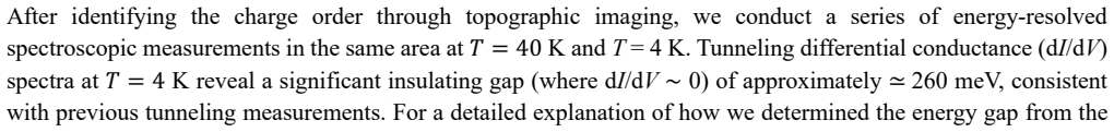
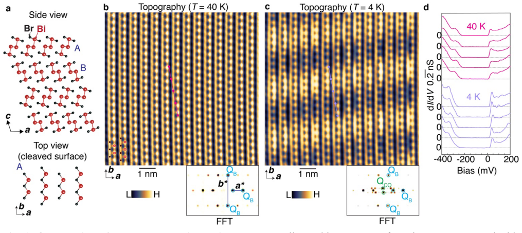
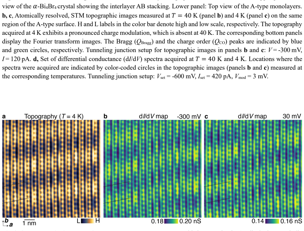
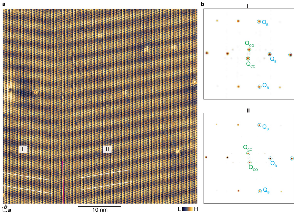
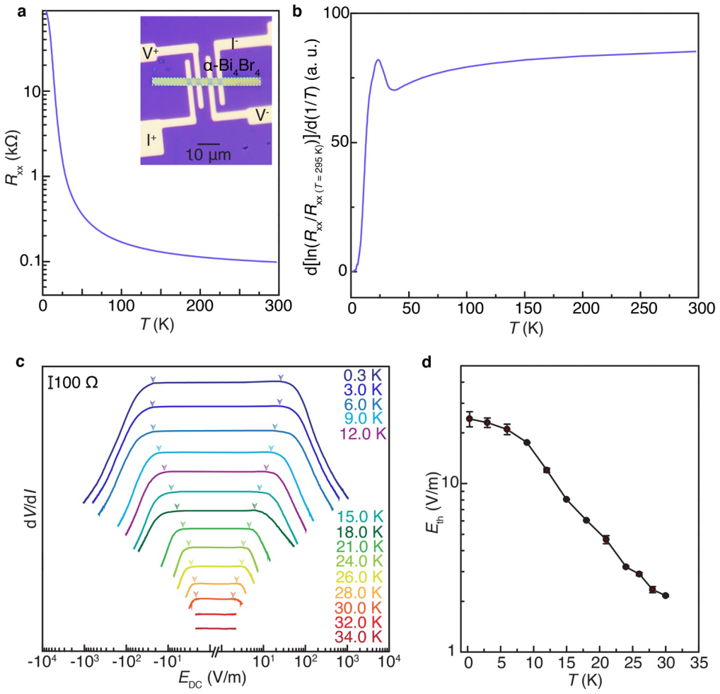
The authors report that Bi4Br4, established as a band insulator with a full gap over the entire Brillouin zone, develops an unexpected unidirectional charge modulation below 40 K. This modulation breaks lattice translation symmetry, adds an energy gap on top of the preexisting insulating gap, and is accompanied by nonlinear electrical transport suggestive of sliding or phason modes. The findings are presented as evidence for a new type of CDW that requires a revised theoretical framework.
What carries the argument
Unidirectional charge modulation observed in STM topographic and spectroscopic maps that breaks lattice translation symmetry inside a fully gapped band insulator.
If this is right
- CDW order can arise without Fermi-surface instabilities or nesting.
- The observed CDW adds a second gap on top of an existing band-insulator gap.
- Nonlinear conduction can appear in fully gapped insulators through CDW-related modes.
- Standard theoretical descriptions of CDWs must be extended to include insulators.
Where Pith is reading between the lines
- Similar CDW states may exist in other fully gapped layered insulators and should be searched for systematically.
- The driving mechanism may involve strong electron-phonon coupling or lattice instabilities decoupled from nesting vectors.
- This phenomenon could influence the design of insulating materials that still host collective electronic modes.
Load-bearing premise
Bi4Br4 is a true band insulator whose gap covers the entire Brillouin zone with no residual Fermi surface or metallic pockets.
What would settle it
Direct ARPES or transport data showing a Fermi surface or metallic states in Bi4Br4 at temperatures below 40 K would falsify the claim that the CDW forms without a Fermi surface.
Figures
read the original abstract
Charge density wave (CDW) implies a periodic modulation of the charge density. Typically observed in metallic systems, CDWs arise from Fermi surface instabilities, resulting in the total or partial gapping of the Fermi surface. Here, we present experimental evidence for a CDW state emerging in a band insulator which has no Fermi surface. The bulk and surface of our material platform, Bi4Br4, is gapped over the entire Brillouin zone. Through topographic and spectroscopic imaging at low temperatures, we unveil an unexpected unidirectional charge modulation in Bi4Br4, breaking the lattice translation symmetry. The CDW develops at temperatures below 40 K and adds an energy gap atop the existing insulating gap of Bi4Br4. Furthermore, our transport measurements reveal nonlinear electrical conduction, a phenomenon conventionally associated with the sliding or phason mode of incommensurate CDWs. These highly unusual observations represent a new type of CDW and demand a new theoretical framework for CDWs.
Editorial analysis
A structured set of objections, weighed in public.
Referee Report
Summary. The manuscript claims to present experimental evidence for a charge density wave (CDW) emerging in the band insulator Bi4Br4, which has no Fermi surface over the full Brillouin zone. Topographic and spectroscopic imaging reveals a unidirectional charge modulation below 40 K that opens an additional gap on top of the insulating gap, while transport measurements show nonlinear electrical conduction suggestive of sliding or phason modes, pointing to a new type of CDW not driven by Fermi-surface instabilities.
Significance. If the central claim holds and Bi4Br4 is confirmed as a complete band insulator with no residual Fermi surface, the result would be significant: it would demonstrate CDW formation outside the conventional metallic Fermi-surface nesting paradigm and would require new theoretical frameworks for CDW physics in insulators.
major comments (1)
- [Abstract] Abstract: The novelty of the claimed CDW rests entirely on Bi4Br4 being a true band insulator with a complete gap and no residual Fermi surface anywhere in the Brillouin zone (bulk or surface). The abstract asserts this premise but supplies no ARPES spectra, DFT band structures, or transport data establishing the absence of any pockets or crossings at EF; without such evidence the departure from conventional CDW physics cannot be evaluated.
Simulated Author's Rebuttal
We thank the referee for their careful reading of our manuscript and for highlighting the importance of clearly establishing the band-insulator character of Bi4Br4. We address the comment point by point below.
read point-by-point responses
-
Referee: [Abstract] Abstract: The novelty of the claimed CDW rests entirely on Bi4Br4 being a true band insulator with a complete gap and no residual Fermi surface anywhere in the Brillouin zone (bulk or surface). The abstract asserts this premise but supplies no ARPES spectra, DFT band structures, or transport data establishing the absence of any pockets or crossings at EF; without such evidence the departure from conventional CDW physics cannot be evaluated.
Authors: We agree that the abstract should more explicitly reference the supporting evidence. The manuscript body contains DFT calculations showing a full gap across the Brillouin zone with no Fermi-surface crossings, together with temperature-dependent transport data confirming activated insulating behavior and the absence of metallic pockets. In the revised manuscript we will update the abstract to cite these results (e.g., “as established by our DFT band-structure calculations and transport measurements”). We note that ARPES is not reported in the present work; the insulating character is instead demonstrated by the combination of DFT and transport. We believe these changes will allow readers to evaluate the claimed departure from conventional CDW physics. revision: yes
Circularity Check
No circularity: experimental observation paper with no derivation chain
full rationale
The paper is an experimental report presenting topographic/spectroscopic imaging and transport data for a unidirectional charge modulation below 40 K in Bi4Br4, together with the assertion that the material is fully gapped. No equations, parameter fits, ansatzes, or self-citations are used to derive the central claim; the observations stand on their own experimental measurements. The load-bearing premise (complete gap, no Fermi surface) is an empirical assertion to be evaluated against the data shown, not a self-referential derivation. This matches the default case of a self-contained experimental result with score 0.
Axiom & Free-Parameter Ledger
axioms (1)
- domain assumption Bi4Br4 is a band insulator gapped over the entire Brillouin zone with no Fermi surface
Reference graph
Works this paper leans on
-
[1]
Lifshitz, I. M. Anomalies of electron characteristics of a metal in the high pressure region. Zh. Eksp. Teor. Fiz. 38, 1569 (1960). 8. Zhou, J.-J., Feng, W., Liu, C.-C., Guan, S. & Yao, Y. Large-gap quantum spin hall insulator in single layer bismuth monobromide Bi4Br4. Nano Lett. 14, 4767 (2014). 9. Zhou, J.-J., Feng, W., Liu, G.-B. & Yao, Y. Topological...
-
[2]
Ortiz, B. R. et al. New kagome prototype materials: discovery of KV3Sb5, RbV3Sb5, and CsV3Sb5. Phys. Rev. Mater. 3, 094407 (2019). 32. Ortiz, B. R. et al. CsV3Sb5: A Z2 Topological Kagome Metal with a Superconducting Ground State. Phys. Rev. Lett. 125, 247002 (2020). 33. Zhong, Y. et al. Nodeless electron pairing in CsV3Sb5-derived kagome superconductors....
2019
discussion (0)
Sign in with ORCID, Apple, or X to comment. Anyone can read and Pith papers without signing in.