Individual Characterization of Fast-Responding Trap States at the NO-Annealed SiO₂/4H-SiC Interface
Pith reviewed 2026-06-29 16:49 UTC · model grok-4.3
The pith
NO-annealing generates individual fast-responding trap states at the SiO₂/4H-SiC interface visible as ring-shaped dissipation patterns.
A machine-rendered reading of the paper's core claim, the machinery that carries it, and where it could break.
Core claim
Ring-shaped dissipation patterns observed exclusively after NO-annealing indicate individual fast-responding trap states generated by nitridation; their energies E_t − E_f, extracted from tip-bias and tip-sample-distance dependence via finite-element electrostatic calculations, extend toward the interfacial conduction-band edge.
What carries the argument
Energy dissipation signal in frequency-modulation atomic force microscopy (FM-AFM) that selectively registers charge exchange on sub-μs timescales, combined with finite-element electrostatic calculations that convert bias and distance data into trap energies.
If this is right
- The detected states contribute to the channel mobility limitation in 4H-SiC MOSFETs.
- Trap energies lie close enough to the conduction-band edge to participate in fast capture and emission processes.
- FM-AFM distinguishes these rapid traps from slower states that dominate conventional capacitance or current measurements.
- Nitridation is confirmed as the source because the patterns are absent without NO-annealing.
Where Pith is reading between the lines
- Refining the NO-anneal recipe to suppress these specific states could raise mobility without sacrificing other interface benefits.
- The same dissipation imaging approach can be tested on alternative passivation treatments or different wide-bandgap interfaces.
- Spatially mapping individual traps offers a route to correlate local defect density with device-to-device variation in threshold voltage or mobility.
Load-bearing premise
The ring-shaped patterns represent individual fast-responding trap states and the electrostatic model accurately maps the measured signals to energies E_t − E_f.
What would settle it
Observation of identical ring-shaped dissipation patterns in a non-NO-annealed control sample, or extraction of trap energies that fall outside the range expected from independent electrical measurements on the same interface.
Figures
read the original abstract
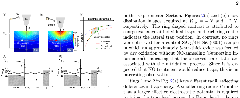
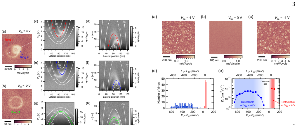
Fast-responding trap states introduced by NO-annealing are suspected to limit the channel mobility of 4H-SiC MOSFETs, yet their microscopic characterization remains challenging because conventional electrical methods are spatially averaged and do not readily isolate such fast processes. Here, we visualize and analyze individual fast-responding trap states at the NO-annealed SiO$_2$/4H-SiC interface using the energy dissipation signal in frequency-modulation atomic force microscopy (FM-AFM), which selectively probes charge-exchange dynamics on sub-$\mu$s time scales. Ring-shaped dissipation patterns were observed in the NO-annealed sample but not in the control sample without NO-annealing, indicating that the detected states are associated with nitridation. Spectroscopic measurements were also performed to determine the dependence of energy dissipation on the tip bias and the tip-sample distance. Combined with finite-element electrostatic calculations, this analysis allowed us to determine trap energies relative to the Fermi level, $E_t - E_f$, and revealed that the trap-energy distribution extends toward the interfacial conduction-band edge. These results provide microscopic evidence that NO-annealing generates fast-responding trap states near the SiO$_2$/4H-SiC interface.
Editorial analysis
A structured set of objections, weighed in public.
Referee Report
Summary. The manuscript reports FM-AFM energy-dissipation imaging of the NO-annealed SiO₂/4H-SiC interface, revealing ring-shaped features absent in non-annealed controls. These are interpreted as individual fast-responding trap states. Bias- and distance-dependent spectroscopy combined with finite-element electrostatic modeling is used to extract trap energies Et−Ef, with the distribution extending toward the conduction-band edge. The central claim is that NO annealing specifically generates these fast traps near the interface.
Significance. If the one-to-one correspondence between ring patterns and individual traps, and the reliability of the FEM inversion, can be established, the work supplies spatially resolved, sub-μs dynamical information on a technologically relevant defect that conventional electrical methods average over. This would be a useful addition to the SiC interface literature.
major comments (2)
- [Results section describing dissipation images] The identification of ring-shaped dissipation features as individual fast-responding traps (rather than extended defects, tip artifacts, or other nitridation-induced structures) is load-bearing for the microscopic claim. The manuscript must supply quantitative statistics (density, size distribution, reproducibility across multiple tips and samples) and explicit controls demonstrating that the rings appear exclusively after NO annealing and vanish under conditions that suppress charge exchange on the relevant timescale.
- [Spectroscopy and finite-element modeling subsection] The conversion of bias- and distance-dependent dissipation data into Et−Ef values rests on finite-element electrostatic modeling whose assumptions (trap depth, dielectric profile, tip radius, oscillation amplitude, charge-state sequence) are not shown to be uniquely constrained by the data. A sensitivity analysis or comparison against alternative models is required; without it the reported energy distribution near the conduction-band edge cannot be considered robust.
minor comments (2)
- [Abstract] The abstract states the method but supplies no numerical values, error estimates, or sample statistics; the main text should include these in the first results paragraph for immediate assessment of data quality.
- [Methods or modeling section] Notation for the energy axis (Et−Ef) should be defined once with explicit reference to the Fermi level position in the SiC and the sign convention used in the FEM output.
Simulated Author's Rebuttal
We thank the referee for the constructive comments and the positive assessment of the potential significance of our work. We address each major comment below and indicate where revisions will be made.
read point-by-point responses
-
Referee: [Results section describing dissipation images] The identification of ring-shaped dissipation features as individual fast-responding traps (rather than extended defects, tip artifacts, or other nitridation-induced structures) is load-bearing for the microscopic claim. The manuscript must supply quantitative statistics (density, size distribution, reproducibility across multiple tips and samples) and explicit controls demonstrating that the rings appear exclusively after NO annealing and vanish under conditions that suppress charge exchange on the relevant timescale.
Authors: We agree that establishing the one-to-one correspondence is central. The manuscript already reports that ring-shaped features are absent in the non-annealed control sample, providing direct evidence of their association with NO annealing. To further strengthen the claim, we will add quantitative statistics on density and size distribution together with reproducibility data across multiple tips and samples. We will also include additional measurements or analysis demonstrating that the dissipation rings vanish when charge exchange is suppressed on the sub-μs timescale (e.g., via bias or frequency conditions outside the relevant window). revision: yes
-
Referee: [Spectroscopy and finite-element modeling subsection] The conversion of bias- and distance-dependent dissipation data into Et−Ef values rests on finite-element electrostatic modeling whose assumptions (trap depth, dielectric profile, tip radius, oscillation amplitude, charge-state sequence) are not shown to be uniquely constrained by the data. A sensitivity analysis or comparison against alternative models is required; without it the reported energy distribution near the conduction-band edge cannot be considered robust.
Authors: We acknowledge that the robustness of the extracted energies would benefit from explicit validation of the modeling assumptions. In the revised manuscript we will add a sensitivity analysis in which the key parameters (trap depth, tip radius, dielectric profile, oscillation amplitude, and charge-state sequence) are varied within physically reasonable ranges; we will show that the conclusion of a trap-energy distribution extending toward the conduction-band edge remains stable. Where appropriate we will also include a brief comparison with a simplified analytical electrostatic model. revision: yes
Circularity Check
No circularity: experimental mapping via standard FEM
full rationale
The paper reports direct experimental observation of ring-shaped dissipation features exclusively in the NO-annealed sample, followed by bias- and distance-dependent spectroscopy. These data are converted to Et-Ef values using finite-element electrostatic calculations, which are standard external modeling tools with no indication that parameters are fitted to the target result or that any equation reduces to a self-definition. No self-citations, ansatzes, or uniqueness theorems are invoked in the provided text to justify the central mapping. The derivation chain therefore remains self-contained against external benchmarks and does not reduce any claimed prediction to its own inputs by construction.
Axiom & Free-Parameter Ledger
axioms (1)
- domain assumption FM-AFM energy dissipation signal selectively probes charge-exchange dynamics on sub-μs time scales
Reference graph
Works this paper leans on
-
[1]
Godignon, J
P. Godignon, J. Biscarrat, M. Tranchesset, R. Lavieville, D. Tournier, P. Brosselard, and J. Montserrat, Break- downvoltagecapabilityofvertical4H–SiCpowerdevices, Mater. Sci. Semicond. Process.178, 108347 (2024)
2024
-
[2]
X. Qian, P. Jiang, and R. Yang, Anisotropic thermal con- ductivity of 4H and 6H silicon carbide measured using time-domain thermoreflectance, Mater. Today Phys.3, 70 (2017)
2017
-
[3]
Kimoto and J
T. Kimoto and J. A. Cooper,Fundamentals of Silicon Carbide Technology: Growth, Characterization, Devices, and Applications, 1st ed. (John Wiley & Sons, 2014)
2014
-
[4]
S. Li, J. Luo, and T. Ye, Investigation of Reducing In- terface State Density in 4H-SiC by Increasing Oxidation Rate, Nanomaterials13, 1568 (2023)
2023
-
[5]
M. Green, E. Gusev, R. Degraeve, and E. Garfunkel, Ul- trathin (<4 nm) SiO2 and Si-O-N Gate Dielectric Lay- ers for Silicon Microelectronics: Understanding the Pro- cessing, Structure, and Physical and Electrical Limits, J. Appl. Phys.90, 10.1063/1.1385803 (2001)
-
[6]
H. Yano, T. Hirao, T. Kimoto, and H. Matsunami, High Channel Mobility in Inversion Layer of SiC MOSFETs for Power Switching Transistors, Jpn. J. Appl. Phys.39, 2008 (2000)
2008
-
[7]
A. M. Vidarsson, D. Haasmann, S. Dimitrijev, and E. Ö. Sveinbjörnsson, Improvement of channel-carrier mobil- ity in 4H-SiC MOSFETs correlated with passivation of very fast interface traps using sodium enhanced oxida- tion, AIP Adv.13, 055126 (2023)
2023
-
[8]
Kil and K
T.-H. Kil and K. Kita, Anomalous band alignment change of SiO2/4H–SiC(0001) and (000–1) MOS capac- itors induced by NO-POA and its possible origin, Appl. Phys. Lett.116, 122103 (2020)
2020
-
[9]
Rozen, S
J. Rozen, S. Dhar, S. K. Dixit, V. V. Afanas’ev, F. O. Roberts, H. L. Dang, S. Wang, S. T. Pantelides, J. R. Williams, and L. C. Feldman, Increase in oxide hole trap density associated with nitrogen incorporation at the SiO2/SiC interface, J. Appl. Phys.103, 124513 (2008)
2008
-
[10]
Chung, C
G. Chung, C. Tin, J. Williams, K. McDonald, R. Chanana, R. Weller, S. Pantelides, L. Feldman, O. Holland, M. Das, and J. Palmour, Improved inversion channel mobility for 4H-SiC MOSFETs following high temperature anneals in nitric oxide, IEEE Electron De- vice Lett.22, 176 (2001)
2001
-
[11]
H.Yoshioka, T.Nakamura,andT.Kimoto,Generationof very fast states by nitridation of the SiO2/SiC interface, J. Appl. Phys.112, 024520 (2012)
2012
-
[12]
Yoshioka, T
H. Yoshioka, T. Nakamura, and T. Kimoto, Characteri- zation of very fast states in the vicinity of the conduction band edge at the SiO2/SiC interface by low temperature conductance measurements, J. Appl. Phys.115, 014502 (2014)
2014
-
[13]
Wen, B.-Y
Y.-X. Wen, B.-Y. Tsui, and K. P. Cheung, Impact of near interface defects on NO annealed SiC MOSFET mobility, Microelectron. Reliab.173, 115841 (2025)
2025
-
[14]
Huang, P
W. Huang, P. Dong, N. Yang, Y. Ma, Q. Xu, C. Fu, M. Huang, Y. Li, Z. Yang, M. Gong, D. He, and Q. He, Effects of nitrogen passivation on the capture cross sec- tion energy distribution of 4H-SiC/SiO 2 interface de- fects and the temperature dependences of leakage cur- rent, Appl. Phys. Lett.127, 122101 (2025)
2025
-
[15]
Tekiel, Y
A. Tekiel, Y. Miyahara, J. M. Topple, and P. Grutter, Room-Temperature Single-Electron Charging Detected by Electrostatic Force Microscopy, ACS Nano7, 4683 (2013)
2013
-
[16]
Miyahara, A
Y. Miyahara, A. Roy-Gobeil, and P. Grutter, Quantum state readout of individual quantum dots by electrostatic 5 force detection, Nanotechnology28, 064001 (2017)
2017
-
[17]
Cowie, T
M. Cowie, T. J. Z. Stock, P. C. Constantinou, N. J. Cur- son, and P. Grütter, Spatially Resolved Dielectric Loss at the Si/SiO2 Interface, Phys. Rev. Lett.132, 256202 (2024)
2024
-
[18]
Uchida, A
Y. Uchida, A. Tamura, and K. Kita, Study on direct NO oxynitridation of 4H-SiC (0001): time dependent change in SiC surface reaction rate and electrical characteristics of SiO(N)/SiC interface, Jpn. J. Appl. Phys. , in press (2026)
2026
-
[19]
A. J. Czarnecki, N. L. Kolev, P. See, N. J. Sullivan, W. A. Behn, N. J. Curson, T. J. Z. Stock, and P. Grütter, Hy- drogen passivation effects on spatially resolved charge trap densities in Si(100)–SiO2, AIP Adv.15, 105024 (2025)
2025
-
[20]
Paszke, S
A. Paszke, S. Gross, F. Massa, A. Lerer, J. Bradbury, G. Chanan, T. Killeen, Z. Lin, N. Gimelshein, L. Antiga, A. Desmaison, A. Kopf, E. Yang, Z. DeVito, M. Rai- son, A. Tejani, S. Chilamkurthy, B. Steiner, L. Fang, J. Bai, and S. Chintala, PyTorch: An Imperative Style, High-Performance Deep Learning Library, inAdvances in Neural Information Processing Sy...
-
[21]
D. Zhai, D. Gao, J. Xiao, X. Gong, J. Yang, Y. Zhao, J. Wang, and J. Lu, Electrical characterization of near- interface traps in thermally oxidized and NO-annealed SiO2 /4H-SiC metal-oxide-semiconductor capacitors, J. Phys. D: Appl. Phys.53, 445102 (2020)
2020
-
[22]
Fiorenza, M
P. Fiorenza, M. Zignale, M. Camalleri, L. Scalia, E. Zanetti, M. Saggio, F. Giannazzo, and F. Roc- caforte, Impact of the NO annealing duration on the SiO2/4H–SiC interface properties in lateral MOSFETs: The energetic profile of the near-interface-oxide traps, Materials Science in Semiconductor Processing169, 107866 (2024)
2024
-
[23]
Y. Xu, X. Zhu, H. D. Lee, C. Xu, S. M. Shubeita, A. C. Ahyi, Y. Sharma, J. R. Williams, W. Lu, S. Ceesay, B. R. Tuttle, A. Wan, S. T. Pantelides, T. Gustafsson, E. L. Garfunkel, and L. C. Feldman, Atomic state and charac- terization of nitrogen at the SiC/SiO2 interface, J. Appl. Phys.115, 033502 (2014)
2014
discussion (0)
Sign in with ORCID, Apple, or X to comment. Anyone can read and Pith papers without signing in.