Co-optimization of spin coherence and valley splitting in Si/SiGe heterostructures
Pith reviewed 2026-06-28 21:42 UTC · model grok-4.3
The pith
Si/SiGe heterostructures with 3-4 nm quantum wells and 50 ppm nuclear spin isotopes support valley splittings above 500 μeV and spin dephasing times over 15 μs.
A machine-rendered reading of the paper's core claim, the machinery that carries it, and where it could break.
Core claim
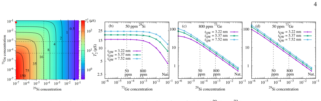
Si/SiGe heterostructures with 3--4 nm wide quantum wells and 73Ge and 29Si concentrations of 50 ppm should support average valley splittings Ev > 500 μeV and spin dephasing times T2* exceeding 15 μs assuming an effective quantum dot area of 700 nm². Sharper Si/SiGe interfaces result in larger valley splittings and longer spin dephasing times.
What carries the argument
Density functional theory calculations that compute valley splitting from the heterostructure potential and hyperfine dephasing rates from the electron wavefunction overlap with nuclear spins in the Si and SiGe layers.
If this is right
- Reducing silicon quantum well width increases valley splitting while the wavefunction penetration into SiGe must be offset by lower isotope concentrations to preserve long T2*.
- Sharper Si/SiGe interfaces simultaneously raise valley splitting and extend spin dephasing times.
- The 3-4 nm well width window with 50 ppm isotopes meets the stated performance targets for 700 nm² dots.
- These heterostructure parameters provide concrete targets for epitaxial growth and isotopic purification in silicon quantum devices.
Where Pith is reading between the lines
- Fabrication efforts should prioritize both precise control of well thickness in the 3-4 nm range and reduction of 73Ge and 29Si below 50 ppm.
- The same wavefunction-engineering approach could be tested in other silicon-based heterostructures to see whether similar co-optimization windows exist.
- If the DFT predictions hold, devices built to these specifications would remove valley and hyperfine limitations as primary obstacles to scaling silicon spin qubits.
Load-bearing premise
Density functional theory calculations accurately predict both the valley splitting and the hyperfine-induced dephasing rates without large systematic errors from exchange-correlation functionals or pseudopotentials.
What would settle it
Fabrication and measurement of Si/SiGe devices with 3-4 nm wells, 50 ppm 73Ge and 29Si, and 700 nm² dots that yield average valley splittings below 500 μeV or T2* below 15 μs.
Figures
read the original abstract
Single electron spins can be used to encode and process information in semiconductor quantum devices. Progress has been hindered by materials challenges, such as the small energy splitting between low-lying valley states and hyperfine coupling to nuclear spins. Here we use density functional theory to optimize the valley splitting and spin dephasing time in realistic Si/SiGe heterostructures. Reductions in the Si quantum well width generally increase the valley splitting. However, in narrow quantum wells, a larger fraction of the electronic wavefunction resides in the SiGe buffer layers, which increases the hyperfine coupling with spinful $^{73}$Ge. Our work shows that Si/SiGe heterostructures with 3~--~4~nm wide quantum wells and $^{73}$Ge and $^{29}$Si concentrations of 50 ppm should support average valley splittings $E_{v}$~$>$~500~$\mu$eV and spin dephasing times $T_2^*$ exceeding 15~$\mu$s assuming an effective quantum dot area of 700 nm$^2$. In addition, sharper Si/SiGe interfaces in general result in larger valley splittings and longer spin dephasing times.
Editorial analysis
A structured set of objections, weighed in public.
Referee Report
Summary. The manuscript uses density functional theory (DFT) simulations of realistic Si/SiGe heterostructures to co-optimize valley splitting Ev and hyperfine-limited spin dephasing time T2* as functions of Si quantum-well width and 73Ge/29Si isotope concentrations. It reports that 3–4 nm wells at 50 ppm spinful-isotope levels yield average Ev > 500 μeV and T2* > 15 μs (for a 700 nm² effective dot area) and that sharper interfaces improve both quantities.
Significance. If the DFT predictions hold, the work supplies concrete, experimentally actionable heterostructure parameters that simultaneously address two leading decoherence channels in Si spin qubits. The explicit treatment of wave-function penetration into the SiGe buffers and the resulting trade-off between well width and hyperfine coupling constitute a useful design insight for the field.
major comments (3)
- [Methods] Methods (DFT setup): No experimental calibration or benchmark of the chosen functional, pseudopotentials, or interface model against measured valley splittings or T2* values in comparable Si/SiGe wells is referenced; any systematic offset in the interface potential or hyperfine matrix elements directly scales the reported optimum (3–4 nm, 50 ppm).
- [Results] Results (T2* calculation): The claim T2* > 15 μs rests on an assumed effective dot area of 700 nm² whose selection and robustness are not justified or varied; because T2* scales inversely with area, this parameter choice is load-bearing for the central numerical claim.
- [Results] Results/Discussion: No error bars, uncertainty quantification, or sensitivity analysis accompany the quoted Ev and T2* thresholds, despite the forward nature of the DFT simulations and the ad-hoc selection of the 50 ppm and 700 nm² targets.
minor comments (2)
- [Abstract] Abstract: The phrase “average valley splittings” is used without defining the averaging procedure (over disorder realizations, positions, or interfaces).
- Notation: Consistent use of “~” versus numerical inequalities for the reported thresholds would improve clarity.
Simulated Author's Rebuttal
We thank the referee for their constructive comments on our manuscript. We address each major point below and have revised the manuscript accordingly where possible to strengthen the presentation of our DFT results.
read point-by-point responses
-
Referee: [Methods] Methods (DFT setup): No experimental calibration or benchmark of the chosen functional, pseudopotentials, or interface model against measured valley splittings or T2* values in comparable Si/SiGe wells is referenced; any systematic offset in the interface potential or hyperfine matrix elements directly scales the reported optimum (3–4 nm, 50 ppm).
Authors: We acknowledge that the manuscript does not include new experimental benchmarks for our specific DFT parameters. The PBE functional and pseudopotentials are standard for Si/SiGe electronic structure calculations and have been validated against experiment in prior literature on valley splittings; we will add explicit citations to these benchmark studies in the revised Methods section. Systematic offsets in absolute Ev or hyperfine values cannot be ruled out without new experiments, but the reported trends versus well width and isotope concentration are expected to be robust. We have made a partial revision by adding the references and a cautionary note on absolute scales. revision: partial
-
Referee: [Results] Results (T2* calculation): The claim T2* > 15 μs rests on an assumed effective dot area of 700 nm² whose selection and robustness are not justified or varied; because T2* scales inversely with area, this parameter choice is load-bearing for the central numerical claim.
Authors: The 700 nm² value was selected as representative of typical lateral dot sizes in electrostatically defined Si/SiGe qubits from the experimental literature. We will revise the manuscript to justify this choice with citations and add a sensitivity analysis showing T2* for dot areas between 400 and 1000 nm². Because T2* scales inversely with the square root of area, this will clarify that the 3–4 nm well and 50 ppm recommendation remains advantageous over a range of realistic dot sizes. revision: yes
-
Referee: [Results] Results/Discussion: No error bars, uncertainty quantification, or sensitivity analysis accompany the quoted Ev and T2* thresholds, despite the forward nature of the DFT simulations and the ad-hoc selection of the 50 ppm and 700 nm² targets.
Authors: We agree that uncertainty quantification was missing. In the revised manuscript we will report error bars obtained from ensemble averages over multiple random isotope placements and interface configurations. We will also add sensitivity plots for isotope concentrations around 50 ppm and for dot areas around 700 nm², identifying the parameter regions satisfying both Ev > 500 μeV and T2* > 15 μs. revision: yes
Circularity Check
No circularity; forward DFT simulations of independent observables
full rationale
The paper's central results are obtained by running density functional theory calculations on Si/SiGe heterostructures with specified well widths, interface sharpness, and isotopic concentrations. Valley splitting Ev and hyperfine dephasing T2* are computed quantities that follow from the electronic structure and nuclear spin interactions; neither is used to fit parameters that are then re-predicted, nor is any step self-definitional or dependent on a load-bearing self-citation chain. The numerical targets (Ev > 500 μeV, T2* > 15 μs) are post-hoc thresholds applied to the simulation outputs rather than inputs that force the result.
Axiom & Free-Parameter Ledger
free parameters (3)
- quantum well width
- isotope concentration
- effective quantum dot area
axioms (2)
- domain assumption DFT with chosen functionals and pseudopotentials correctly captures valley splitting and wavefunction overlap into SiGe buffers
- domain assumption Hyperfine dephasing is dominated by 73Ge and 29Si nuclei with rates scaling linearly with wavefunction probability density in those layers
Reference graph
Works this paper leans on
-
[1]
Kjaergaard, M
M. Kjaergaard, M. E. Schwartz, J. Braumüller, P. Krantz, J. I.- J. Wang, S. Gustavsson, and W. D. Oliver, Superconducting qubits: Current state of play, Annu. Rev. Condens. Matter Phys. 11, 369 (2020)
2020
-
[2]
C. D. Bruzewicz, J. Chiaverini, R. McConnell, and J. M. Sage, Trapped-ion quantum computing: Progress and challenges, Appl. Phys. Rev.6, 021314 (2019)
2019
-
[3]
Childress and R
L. Childress and R. Hanson, Diamond nv centers for quantum computing and quantum networks, MRS Bull.38, 134 (2013)
2013
-
[4]
Burkard, T
G. Burkard, T. D. Ladd, A. Pan, J. M. Nichol, and J. R. Petta, Semiconductor spin qubits, Rev. Mod. Phys.95, 025003 (2023)
2023
-
[5]
Huang, C
W. Huang, C. H. Yang, K. W. Chan, T. Tanttu, B. Hensen, R. C. C. Leon, M. A. Fogarty, J. C. C. Hwang, F. E. Hud- son, K. M. Itoh, A. Morello, A. Laucht, and A. S. Dzurak, Fi- delity benchmarks for two-qubit gates in silicon, Nature569, 532 (2019)
2019
-
[6]
A. R. Mills, C. R. Guinn, M. J. Gullans, A. J. Sigillito, M. M. Feldman, E. Nielsen, and J. R. Petta, Two-qubit silicon quantum processor with operation fidelity exceeding 99%, Sci. Adv.8, eabn5130 (2022)
2022
-
[7]
Noiri, K
A. Noiri, K. Takeda, T. Nakajima, T. Kobayashi, A. Sammak, G. Scappucci, and S. Tarucha, Fast universal quantum gate above the fault-tolerance threshold in silicon, Nature601, 338 (2022)
2022
-
[8]
X. Xue, M. Russ, N. Samkharadze, B. Undseth, A. Sammak, G. Scappucci, and L. M. Vandersypen, Quantum logic with spin qubits crossing the surface code threshold, Nature601, 343 (2022)
2022
-
[9]
W. Ha, S. D. Ha, M. D. Choi, Y . Tang, A. E. Schmitz, M. P. Levendorf, K. Lee, J. M. Chappell, T. S. Adams, D. R. Hulbert, E. Acuna, R. S. Noah, J. W. Matten, M. P. Jura, J. A. Wright, M. T. Rakher, and M. G. Borselli, A Flexible Design Platform for Si/SiGe Exchange-Only Qubits with Low Disorder, Nano Lett.22, 1443 (2022)
2022
-
[10]
Neyens, O
S. Neyens, O. K. Zietz, T. F. Watson, F. Luthi, A. Nethwewala, H. C. George, E. Henry, M. Islam, A. J. Wagner, F. Borjans, E. J. Connors, J. Corrigan, M. J. Curry, D. Keith, R. Kotl- yar, L. F. Lampert, M. T. M ˛ adzik, K. Millard, F. A. Mo- hiyaddin, S. Pellerano, R. Pillarisetty, M. Ramsey, R. Savyt- skyy, S. Schaal, G. Zheng, J. Ziegler, N. C. Bishop, ...
2024
-
[11]
A. J. Weinstein, M. D. Reed, A. M. Jones, R. W. Andrews, D. Barnes, J. Z. Blumoff, L. E. Euliss, K. Eng, B. H. Fong, S. D. Ha, D. R. Hulbert, C. A. C. Jackson, M. Jura, T. E. Keat- ing, J. Kerckhoff, A. A. Kiselev, J. Matten, G. Sabbir, A. Smith, J. Wright, M. T. Rakher, T. D. Ladd, and M. G. Borselli, Univer- sal logic with encoded spin qubits in silicon...
2023
-
[12]
B. Undseth, N. Meggiato, Y .-H. Wu, S. R. Katiraee-Far, L. Try- puten, S. L. de Snoo, D. D. Esposti, G. Scappucci, E. Greplová, and L. M. K. Vandersypen, Weight-four parity checks with sil- icon spin qubits, (2026), arXiv:2601.23267
arXiv 2026
-
[13]
Abrahamet al., A digitally controlled silicon quantum pro- cessing unit, (2026), arXiv:2604.16216
M. Abrahamet al., A digitally controlled silicon quantum pro- cessing unit, (2026), arXiv:2604.16216
Pith/arXiv arXiv 2026
-
[14]
Zheng, N
G. Zheng, N. Samkharadze, M. L. Noordam, N. Kalhor, D. Brousse, A. Sammak, G. Scappucci, and L. M. K. Vander- sypen, Rapid gate-based spin read-out in silicon using an on- chip resonator, Nat. Nanotechnol.14, 742 (2019)
2019
-
[15]
Borjans, X
F. Borjans, X. Mi, and J. Petta, Spin digitizer for high-fidelity readout of a cavity-coupled silicon triple quantum dot, Phys. Rev. Applied15, 044052 (2021)
2021
-
[16]
X. Mi, M. Benito, S. Putz, D. M. Zajac, J. M. Taylor, G. Burkard, and J. R. Petta, A coherent spin-photon interface in silicon, Nature555, 599 (2018)
2018
-
[17]
Borjans, X
F. Borjans, X. G. Croot, X. Mi, M. J. Gullans, and J. R. Petta, Resonant microwave-mediated interactions between dis- tant electron spins, Nature577, 195 (2020)
2020
-
[18]
Samkharadze, G
N. Samkharadze, G. Zheng, N. Kalhor, D. Brousse, A. Sam- mak, U. C. Mendes, A. Blais, G. Scappucci, and L. M. K. Van- dersypen, Strong spin-photon coupling in silicon, Science359, 1123 (2018)
2018
-
[19]
A. J. Landig, J. V . Koski, P. Scarlino, U. C. Mendes, A. Blais, C. Reichl, W. Wegscheider, A. Wallraff, K. Ensslin, and T. Ihn, Coherent spin-photon coupling using a resonant ex- change qubit, Nature560, 179 (2018)
2018
-
[20]
Dijkema, X
J. Dijkema, X. Xue, P. Harvey-Collard, M. Rimbach-Russ, S. L. de Snoo, G. Zheng, G. Scappucci, and L. M. K. Vandersypen, Cavity-mediated iswap oscillations between distant spins, Na- ture Phys.21, 168 (2025)
2025
-
[21]
J. R. Petta, A. C. Johnson, J. M. Taylor, E. Laird, A. Yacoby, M. D. Lukin, C. M. Marcus, M. P. Hanson, and A. C. Gossard, Coherent manipulation of coupled electron spins in semicon- ductor quantum dots., Science309, 2180 (2005)
2005
-
[22]
J. T. Muhonen, J. P. Dehollain, A. Laucht, F. E. Hudson, R. Kalra, T. Sekiguchi, K. M. Itoh, D. N. Jamieson, J. C. Mc- Callum, A. S. Dzurak, and A. Morello, Storing quantum infor- mation for 30 seconds in a nanoelectronic device., Nat. Nan- otechnol.9, 986 (2014)
2014
-
[23]
K. Eng, T. D. Ladd, A. Smith, M. G. Borselli, A. A. Kiselev, B. H. Fong, K. S. Holabird, T. M. Hazard, B. Huang, P. W. Deelman, I. Milosavljevic, A. E. Schmitz, R. S. Ross, M. F. Gyure, and A. T. Hunter, Isotopically enhanced triple-quantum- dot qubit, Sci. Adv.1, 1500214 (2015)
2015
-
[24]
Moutanabbir, S
O. Moutanabbir, S. Assali, A. Attiaoui, G. Daligou, P. Daoust, P. D. Vecchio, S. Koelling, L. Luo, and N. Rotaru, Nuclear Spin-Depleted, Isotopically Enriched 70Ge/28Si70Ge Quantum Wells, Adv. Matl.36, 2305703 (2024)
2024
-
[25]
Schäffler, High-mobility Si and Ge structures, Semicond
F. Schäffler, High-mobility Si and Ge structures, Semicond. Sci. Technol.12, 1515 (1997)
1997
-
[26]
E. H. Chen, K. Raach, A. Pan, A. A. Kiselev, E. Acuna, J. Z. Blumoff, T. Brecht, M. D. Choi, W. Ha, D. R. Hulbert, M. P. Jura, T. E. Keating, R. Noah, B. Sun, B. J. Thomas, M. G. Borselli, C. Jackson, M. T. Rakher, and R. S. Ross, Detuning Axis Pulsed Spectroscopy of Valley-Orbital States in Si / Si - Ge Quantum Dots, Phys. Rev. Applied15, 044033 (2021)
2021
-
[27]
V olmer, T
M. V olmer, T. Struck, A. Sala, B. Chen, M. Oberländer, T. Of- fermann, R. Xue, L. Visser, J.-S. Tu, S. Trellenkamp, L. Cywin- ski, H. Bluhm, and L. R. Schreiber, Mapping of valley splitting by conveyor-mode spin-coherent electron shuttling, npj Quan- tum Inf.10, 61 (2024)
2024
-
[28]
Tariq and X
B. Tariq and X. Hu, Impact of the valley orbit coupling on ex- change gate for spin qubits in silicon, npj Quantum Inf.8, 53 (2022)
2022
-
[29]
Loss and D
D. Loss and D. P. DiVincenzo, Quantum computation with quantum dots, Phys. Rev. A57, 120 (1998)
1998
-
[30]
T. B. Boykin, G. Klimeck, M. Friesen, S. N. Coppersmith, P. von Allmen, F. Oyafuso, and S. Lee, Valley splitting in low- density quantum-confined heterostructures studied using tight- binding models, Phys. Rev. B70, 165325 (2004)
2004
-
[31]
Friesen and S
M. Friesen and S. N. Coppersmith, Theory of valley-orbit cou- pling in a Si/SiGe quantum dot, Phys. Rev. B81, 115324 (2010). 6
2010
-
[32]
McJunkin, E
T. McJunkin, E. MacQuarrie, L. Tom, S. Neyens, J. Dodson, B. Thorgrimsson, J. Corrigan, H. E. Ercan, D. Savage, M. La- gally,et al., Valley splittings in Si/SiGe quantum dots with a germanium spike in the silicon well, Phys. Rev. B104, 085406 (2021)
2021
-
[33]
McJunkin, B
T. McJunkin, B. Harpt, Y . Feng, M. P. Losert, R. Rahman, J. P. Dodson, M. A. Wolfe, D. E. Savage, M. G. Lagally, S. N. Cop- persmith, M. Friesen, R. Joynt, and M. A. Eriksson, SiGe quan- tum wells with oscillating Ge concentrations for quantum dot qubits, Nat. Commun.13, 7777 (2022)
2022
-
[34]
Zunger, S.-H
A. Zunger, S.-H. Wei, L. G. Ferreira, and J. E. Bernard, Special quasirandom structures, Phys. Rev. Lett.65, 353 (1990)
1990
-
[35]
van de Walle, M
A. van de Walle, M. Asta, and G. Ceder, The alloy theoretic automated toolkit: A user guide, Calphad26, 539 (2002)
2002
-
[36]
Kresse and J
G. Kresse and J. Hafner, Ab initio molecular dynamics for liq- uid metals, Phys. Rev. B47, 558 (1993)
1993
-
[37]
Kresse and J
G. Kresse and J. Furthmuller, Efficiency of ab-initio total en- ergy calculations for metals and semiconductors using a plane- wave basis set, Comput. Mater. Sci.6, 15 (1996)
1996
-
[38]
J. P. Perdew, A. Ruzsinszky, G. I. Csonka, O. A. Vydrov, G. E. Scuseria, L. A. Constantin, X. Zhou, and K. Burke, Restoring the density-gradient expansion for exchange in solids and sur- faces, Phys. Rev. Lett.100, 136406 (2008)
2008
-
[39]
J. P. Dismukes, Ekstrom, and R. J. Paff, Lattice parameter and density in germanium-silicon alloys, J. Phys. Chem.68, 3021 (1964)
1964
-
[40]
J. M. Taylor, J. R. Petta, A. C. Johnson, A. Yacoby, C. M. Mar- cus, and M. D. Lukin, Relaxation, dephasing, and quantum con- trol of electron spins in double quantum dots, Phys. Rev. B76, 035315 (2007)
2007
-
[41]
P. E. Blochl, Projector augmented-wave method, Phys. Rev. B 50, 17953 (1994)
1994
-
[42]
P. E. Blochl, First-principles calculations of defects in oxygen- deficient silica exposed to hydrogen, Phys. Rev. B62, 6158 (2000)
2000
-
[43]
A. R. Mills, D. M. Zajac, M. J. Gullans, F. J. Schupp, T. M. Hazard, and J. R. Petta, Shuttling a single charge across a one- dimensional array of silicon quantum dots, Nat. Commun.10, 1063 (2019)
2019
-
[44]
Anderson and M
C. Anderson and M. Gyure, private communication,
-
[45]
D. M. Zajac, T. M. Hazard, X. Mi, E. Nielsen, and J. R. Petta, Scalable gate architecture for a one-dimensional array of semi- conductor spin qubits, Phys. Rev. Applied6, 054013 (2016)
2016
-
[46]
P. W. Deelman, L. F. Edge, and C. A. Jackson, Metamorphic materials for quantum computing, MRS Bull.41, 224 (2016)
2016
-
[47]
Scappucci, C
G. Scappucci, C. Kloeffel, F. A. Zwanenburg, D. Loss, M. My- ronov, J.-J. Zhang, S. De Franceschi, G. Katsaros, and M. Veld- horst, The germanium quantum information route, Nat. Rev. Mater.6, 926 (2021)
2021
-
[48]
Cvitkovich, P
L. Cvitkovich, P. Stano, C. Wilhelmer, D. Waldhor, D. Loss, Y .-M. Niquet, and T. Grasser, Coherence limit due to hyperfine interaction with nuclei in the barrier material of Si spin qubits, Phys. Rev. Applied22, 064089 (2024)
2024
discussion (0)
Sign in with ORCID, Apple, or X to comment. Anyone can read and Pith papers without signing in.