Breaking the width-scaling limit in high-performance atomically thin 2D nanoribbon transistors
Pith reviewed 2026-06-28 08:19 UTC · model grok-4.3
The pith
Monolayer and bilayer MoS2 nanoribbon transistors increase on-current density by up to 230 percent as channel width shrinks to 15 nm.
A machine-rendered reading of the paper's core claim, the machinery that carries it, and where it could break.
Core claim
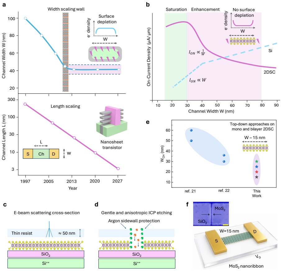
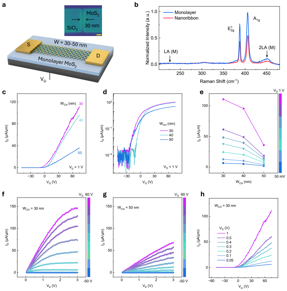
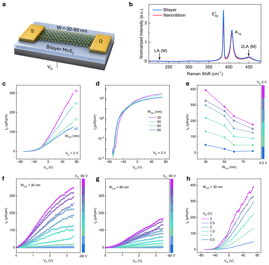
In contrast to the conventional scaling rule of degradation of current density upon width scaling, our atomically-thin monolayer and bilayer molybdenum disulfide nanoribbon transistors exhibit enhancement of on-current density of up to 230% and 170%, respectively, followed by a saturation for the narrowest channels down to 15 nm. The ultra-narrow nanoribbon transistors maintain the highest on/off ratios reported so far for similar device dimensions, with improved mobility and threshold-voltage stability, indicating reduced edge scattering and depletion with a stronger electrostatic control.
What carries the argument
Ultra-scaled two-dimensional molybdenum disulfide nanoribbon transistors that maintain atomic thickness while reducing channel width.
If this is right
- Transistor channel widths can continue to shrink without the expected drop in drive current.
- On-current density gains at narrow widths improve switching speed and power efficiency.
- Higher on-off ratios at 15 nm widths support low-leakage operation in dense circuits.
- Improved mobility and threshold stability reduce variability in scaled devices.
- The saturation of gains at the narrowest widths defines a practical lower limit for this approach.
Where Pith is reading between the lines
- The same nanoribbon strategy may extend to other transition-metal dichalcogenides to test whether the current-density upturn is material-specific.
- Circuit-level simulations could check whether the measured per-device gains translate to faster logic gates or memory cells at fixed power.
- Temperature-dependent measurements on the same devices would separate scattering reduction from electrostatic effects.
- Integration with high-k dielectrics on top and bottom could further amplify the electrostatic control reported here.
Load-bearing premise
The observed rise in current density is produced by the nanoribbon geometry and material properties themselves rather than by uncontrolled differences in contacts or processing steps.
What would settle it
Fabricating matched sets of nanoribbon devices with identical contacts and dielectric interfaces but deliberately varied edge disorder, then measuring whether current density still rises at narrower widths.
Figures
read the original abstract
State-of-the-art transistors have been successfully scaled the gate lengths and channel thicknesses down to 5 nm for high-performance and energy-efficient information processing. However, reducing channel width below 40-50 nm remains a bottleneck, as dangling bonds, edge disorder, and lateral depletion suppress drive current and degrade device performance. Here, we break this width-scaling wall using ultra-scaled two-dimensional semiconductor (2DSC) nanoribbon transistors down to 15 nm. In contrast to the conventional scaling rule of degradation of current density upon width scaling, our atomically-thin monolayer and bilayer molybdenum disulfide nanoribbon transistors exhibit enhancement of on-current density of up to 230% and 170%,respectively, followed by a saturation for the narrowest channels down to 15 nm. The ultra-narrow nanoribbon transistors maintain the highest on/off ratios reported so far for similar device dimensions, with improved mobility and threshold-voltage stability, indicating reduced edge scattering and depletion with a stronger electrostatic control. These findings lead to a breakthrough in width scaling rules using 2DSC nanoribbons with enhanced performance at narrower channel widths, which is promising for the ultimate scaling of transistors.
Editorial analysis
A structured set of objections, weighed in public.
Referee Report
Summary. The manuscript reports the fabrication of monolayer and bilayer MoS2 nanoribbon field-effect transistors with physical channel widths scaled to 15 nm. Contrary to the conventional expectation of current-density degradation below ~40-50 nm widths, the authors claim measured on-current densities increase by up to 230% (monolayer) and 170% (bilayer) with decreasing width before saturating, while on/off ratios remain the highest reported for comparable dimensions, accompanied by improved mobility and threshold-voltage stability. These observations are attributed to reduced edge scattering and stronger electrostatic control in the atomically thin nanoribbons.
Significance. If the on-current-density gains are shown to be intrinsic after rigorous exclusion of contact and metrology artifacts, the result would constitute a notable experimental advance in 2D semiconductor scaling, directly addressing the width-scaling bottleneck that has limited high-performance nanoribbon devices. The work supplies concrete device data at the 15 nm width frontier, which is valuable even if the mechanistic interpretation requires refinement.
major comments (3)
- [Abstract and Results] Abstract and Results section: The central claim that J_on (= I_d/W) rises 230%/170% with decreasing width rests on the assumption that contact resistance is either width-independent or has been subtracted; no transfer-length-method data, width-dependent R_c measurements, or contact-resistance correction procedure is described, leaving open the possibility that narrower ribbons received systematically lower R_c due to fabrication variations.
- [Device fabrication and metrology] Device fabrication and metrology subsection: Physical channel width (required for accurate J_on at 15 nm) is not stated to have been measured by AFM or SEM with quantified uncertainty; if nominal lithographic widths were used instead, the reported density increase could be inflated by systematic overestimation of W in narrower devices.
- [Results] Results section (saturation behavior): The observed saturation of J_on at the narrowest (15 nm) channels is interpreted as the onset of intrinsic edge-scattering reduction, yet the same saturation is equally consistent with a transition to contact-limited transport; without width-series contact-resistance data or four-probe measurements, this alternative cannot be excluded.
minor comments (2)
- [Abstract] The abstract states quantitative percentages without accompanying error bars, device counts, or yield statistics; these should be added to the main text or a supplementary table for reproducibility.
- [Methods and Figure captions] Figure captions and methods should explicitly state the gate dielectric, annealing conditions, and measurement temperature, as these parameters can influence apparent mobility and V_th stability.
Simulated Author's Rebuttal
We thank the referee for the detailed and constructive comments. We address each major comment below and agree that clarifications on contact resistance and metrology will improve the manuscript. We will revise accordingly.
read point-by-point responses
-
Referee: [Abstract and Results] Abstract and Results section: The central claim that J_on (= I_d/W) rises 230%/170% with decreasing width rests on the assumption that contact resistance is either width-independent or has been subtracted; no transfer-length-method data, width-dependent R_c measurements, or contact-resistance correction procedure is described, leaving open the possibility that narrower ribbons received systematically lower R_c due to fabrication variations.
Authors: We acknowledge the importance of this point. All nanoribbon devices were fabricated simultaneously on the same substrate with identical contact metallization and geometry, minimizing systematic variations in contact resistance. Nevertheless, to rigorously address this concern, we will add transfer-length-method (TLM) measurements for different widths in the revised manuscript to explicitly demonstrate that contact resistance does not vary significantly with width and does not account for the observed J_on enhancement. revision: yes
-
Referee: [Device fabrication and metrology] Device fabrication and metrology subsection: Physical channel width (required for accurate J_on at 15 nm) is not stated to have been measured by AFM or SEM with quantified uncertainty; if nominal lithographic widths were used instead, the reported density increase could be inflated by systematic overestimation of W in narrower devices.
Authors: We agree that accurate physical width measurement is essential. The widths reported were determined from high-resolution SEM imaging post-fabrication, with an estimated uncertainty of ±1.5 nm based on multiple measurements per device. We will include these metrology details, including representative SEM images and the uncertainty quantification, in the revised manuscript to confirm the validity of the J_on calculations. revision: yes
-
Referee: [Results] Results section (saturation behavior): The observed saturation of J_on at the narrowest (15 nm) channels is interpreted as the onset of intrinsic edge-scattering reduction, yet the same saturation is equally consistent with a transition to contact-limited transport; without width-series contact-resistance data or four-probe measurements, this alternative cannot be excluded.
Authors: This is a valid alternative interpretation. While the high on/off ratios and improved mobility support our interpretation of reduced edge effects, we cannot fully exclude contact-limited behavior without additional data. We will revise the discussion to present both possibilities and include any available four-probe data or note the need for further experiments to distinguish the mechanisms. revision: partial
Circularity Check
No circularity: purely experimental report of measured device characteristics
full rationale
The manuscript presents direct experimental measurements of on-current density, on/off ratio, mobility, and threshold voltage in fabricated MoS2 nanoribbon transistors as a function of channel width. No derivation chain, fitted model, predictive equation, or ansatz is claimed or used; the central result is the observed trend in measured quantities, not a reduction of any quantity to itself via self-definition or self-citation. Self-contained experimental data require no external uniqueness theorems or prior author work to stand. Score remains 0 under the rule that honest non-findings are expected for papers without derivation steps.
Axiom & Free-Parameter Ledger
Reference graph
Works this paper leans on
-
[1]
Nat Electron 8, 871–871 (2025)
100 years of field-effect transistors. Nat Electron 8, 871–871 (2025)
2025
-
[2]
Cao, W. et al. The future transistors. Nature 620, 501–515 (2023)
2023
-
[3]
Islam, M. M. et al. Challenges and prospects of 2D electronics for future monolithic complementary field-effect transistors. Nat Commun 17, 3586 (2026)
2026
-
[4]
& Yin, H
Zhang, Q., Zhang, Y., Luo, Y. & Yin, H. New structure transistors for advanced technology node CMOS ICs. Natl Sci Rev 11, nwae008 (2024)
2024
-
[5]
& Datta, S
Salahuddin, S., Ni, K. & Datta, S. The era of hyper-scaling in electronics. Nat Electron 1, 442–450 (2018)
2018
-
[6]
Wang, S. et al. Two-dimensional devices and integration towards the silicon lines. Nat. Mater. 21, 1225–1239 (2022)
2022
-
[7]
Jiang, J. et al. Advancing 2D CMOS electronics with high-performance p-type transistors. Nat Commun 16, 10233 (2025)
2025
-
[8]
& Zhang, H
Chhowalla, M., Jena, D. & Zhang, H. Two-dimensional semiconductors for transistors. Nat Rev Mater 1, 16052 (2016)
2016
-
[9]
& Hone, J
Akinwande, D., Petrone, N. & Hone, J. Two-dimensional flexible nanoelectronics. Nat Commun 5, 5678 (2014)
2014
-
[10]
& Zhou, P
Zeng, S., Liu, C. & Zhou, P. Transistor engineering based on 2D materials in the post-silicon era. Nat Rev Electr Eng 1, 335–348 (2024)
2024
-
[11]
Pendurthi, R. et al. Monolithic three-dimensional integration of complementary two-dimensional field-effect transistors. Nat. Nanotechnol. 19, 970–977 (2024)
2024
-
[12]
Akinwande, D. et al. Graphene and two-dimensional materials for silicon technology. Nature 573, 507–518 (2019)
2019
-
[13]
Jayachandran, D. et al. Three-dimensional integration of two-dimensional field-effect transistors. Nature 625, 276– 281 (2024)
2024
-
[14]
& Li, L.-J
Zheng, F., Meng, W. & Li, L.-J. Continue the Scaling of Electronic Devices with Transition Metal Dichalcogenide Semiconductors. Nano Lett. 25, 3683–3691 (2025)
2025
-
[15]
Ao, M. et al. A RISC-V 32-bit microprocessor based on two-dimensional semiconductors. Nature 640, 654–661 (2025)
2025
-
[16]
Ghosh, S. et al. A complementary two-dimensional material-based one instruction set computer. Nature 642, 327– 335 (2025)
2025
-
[17]
Du, M. et al. Scaled crystalline antimony ohmic contacts for two-dimensional transistors. Nat Electron 8, 1191–1200 (2025)
2025
-
[18]
Sakib, N. U. et al. High-performance molybdenum disulfide transistors with channel and contact lengths below 35 nm. Nat Electron 8, 1201–1210 (2025)
2025
-
[19]
Mallik, S. K. et al. Salt-assisted growth of monolayer MoS2 for high-performance hysteresis-free field-effect transistor. J. Appl. Phys. 129, 145106 (2021)
2021
-
[20]
Duan, X. et al. MoS2 Nanoribbon Transistor for Logic Electronics. IEEE Transactions on Electron Devices 69, 3433– 3438 (2022)
2022
-
[21]
Chen, S. et al. Monolayer MoS2 Nanoribbon Transistors Fabricated by Scanning Probe Lithography. Nano Lett. 19, 2092–2098 (2019)
2092
-
[22]
L., Lau, C
Kotekar-Patil, D., Deng, J., Wong, S. L., Lau, C. S. & Goh, K. E. J. Single layer MoS2 nanoribbon field effect transistor. Appl. Phys. Lett. 114, 013508 (2019)
2019
-
[23]
Liu, Y. et al. Promises and prospects of two-dimensional transistors. Nature 591, 43–53 (2021)
2021
-
[24]
Liu, H., Gu, J. & Ye, P. D. MoS2 Nanoribbon Transistors: Transition From Depletion Mode to Enhancement Mode by Channel-Width Trimming. IEEE Electron Device Letters 33, 1273–1275 (2012)
2012
-
[25]
& Murali, R
Yang, Y. & Murali, R. Impact of Size Effect on Graphene Nanoribbon Transport. IEEE Electron Device Letters 31, 237–239 (2010). 16
2010
-
[26]
Chen, Y. et al. Fabrication of MoSe2 nanoribbons via an unusual morphological phase transition. Nat Commun 8, 15135 (2017)
2017
-
[27]
Hoque, Md. A. et al. Ultranarrow Semiconductor WS2 Nanoribbon Field-Effect Transistors. Nano Lett. 25, 1750– 1757 (2025)
2025
-
[28]
Verre, R. et al. Transition metal dichalcogenide nanodisks as high-index dielectric Mie nanoresonators. Nat. Nanotechnol. 14, 679–683 (2019)
2019
-
[29]
Munkhbat, B. et al. Transition metal dichalcogenide metamaterials with atomic precision. Nat Commun 11, 4604 (2020)
2020
-
[30]
Saunders, A. P. et al. Direct Exfoliation of Nanoribbons from Bulk van der Waals Crystals. Small 20, 2403504 (2024)
2024
-
[31]
Li, X. et al. Width-dependent continuous growth of atomically thin quantum nanoribbons from nanoalloy seeds in chalcogen vapor. Nat Commun 15, 10080 (2024)
2024
-
[32]
Ma, Z. et al. Lattice-guided growth of dense arrays of aligned transition metal dichalcogenide nanoribbons with high catalytic reactivity. Science Advances 11, eadr8046 (2025)
2025
-
[33]
Li, X. et al. Nickel particle–enabled width-controlled growth of bilayer molybdenum disulfide nanoribbons. Science Advances 7, eabk1892 (2021)
2021
-
[34]
Cain, J. D. et al. Ultranarrow TaS2 Nanoribbons. Nano Lett. 21, 3211–3217 (2021)
2021
-
[35]
& Kitaura, R
Canton-Vitoria, R., Hotta, T., Xue, M., Zhang, S. & Kitaura, R. Synthesis and Characterization of Transition Metal Dichalcogenide Nanoribbons Based on a Controllable O2 Etching. JACS Au 3, 775–784 (2023)
2023
-
[36]
Tanaka, T. et al. Confined Growth of Few-Nanometer MoS2 Nanoribbons with Optical Anisotropy in Insulating Nanotubes. Nano Lett. 25, 14645–14652 (2025)
2025
-
[37]
Mallik, S. K. et al. Polarized Moiré Phonon and Strain-Coupled Phonon Renormalization in Twisted Bilayer MoS2. J. Phys. Chem. C 126, 15788–15794 (2022)
2022
-
[38]
Mignuzzi, S. et al. Effect of disorder on Raman scattering of single-layer MoS2. Phys. Rev. B 91, 195411 (2015)
2015
-
[39]
Li, X. et al. Performance Potential and Limit of MoS2 Transistors. Advanced Materials 27, 1547–1552 (2015)
2015
-
[40]
Yalon, E. et al. Energy Dissipation in Monolayer MoS2 Electronics. Nano Lett. 17, 3429–3433 (2017)
2017
-
[41]
Fathipour, S. et al. Synthesized multiwall MoS2 nanotube and nanoribbon field-effect transistors. Appl. Phys. Lett. 106, 022114 (2015)
2015
-
[42]
P., Bashir, R
Chen, S., Zhang, Y., King, W. P., Bashir, R. & van der Zande, A. M. Edge-Passivated Monolayer WSe2 Nanoribbon Transistors. Advanced Materials 36, 2313694 (2024)
2024
-
[43]
Liu, H., Neal, A. T. & Ye, P. D. Channel Length Scaling of MoS2 MOSFETs. ACS Nano 6, 8563–8569 (2012)
2012
-
[44]
Peña, T. et al. Scaling High-Performance Nanoribbon Transistors with Monolayer Transition Metal Dichalcogenides. arXiv.org https://arxiv.org/abs/2509.09964v2 (2025)
Pith/arXiv arXiv 2025
-
[45]
Lan, H.-Y. et al. Scaling Two-Dimensional Semiconductor Nanoribbons for High-Performance Electronics. arXiv.org https://arxiv.org/abs/2601.13696v3 (2026)
Pith/arXiv arXiv 2026
discussion (0)
Sign in with ORCID, Apple, or X to comment. Anyone can read and Pith papers without signing in.