An ultra-wide-bandgap semiconductor photodetector for linear measurement of bright sub-bandgap light
Pith reviewed 2026-06-27 20:51 UTC · model grok-4.3
The pith
AlN photodetectors achieve non-saturating linear response to blue light above 40 W/cm² via deep-level defects at the Schottky junction.
A machine-rendered reading of the paper's core claim, the machinery that carries it, and where it could break.
Core claim
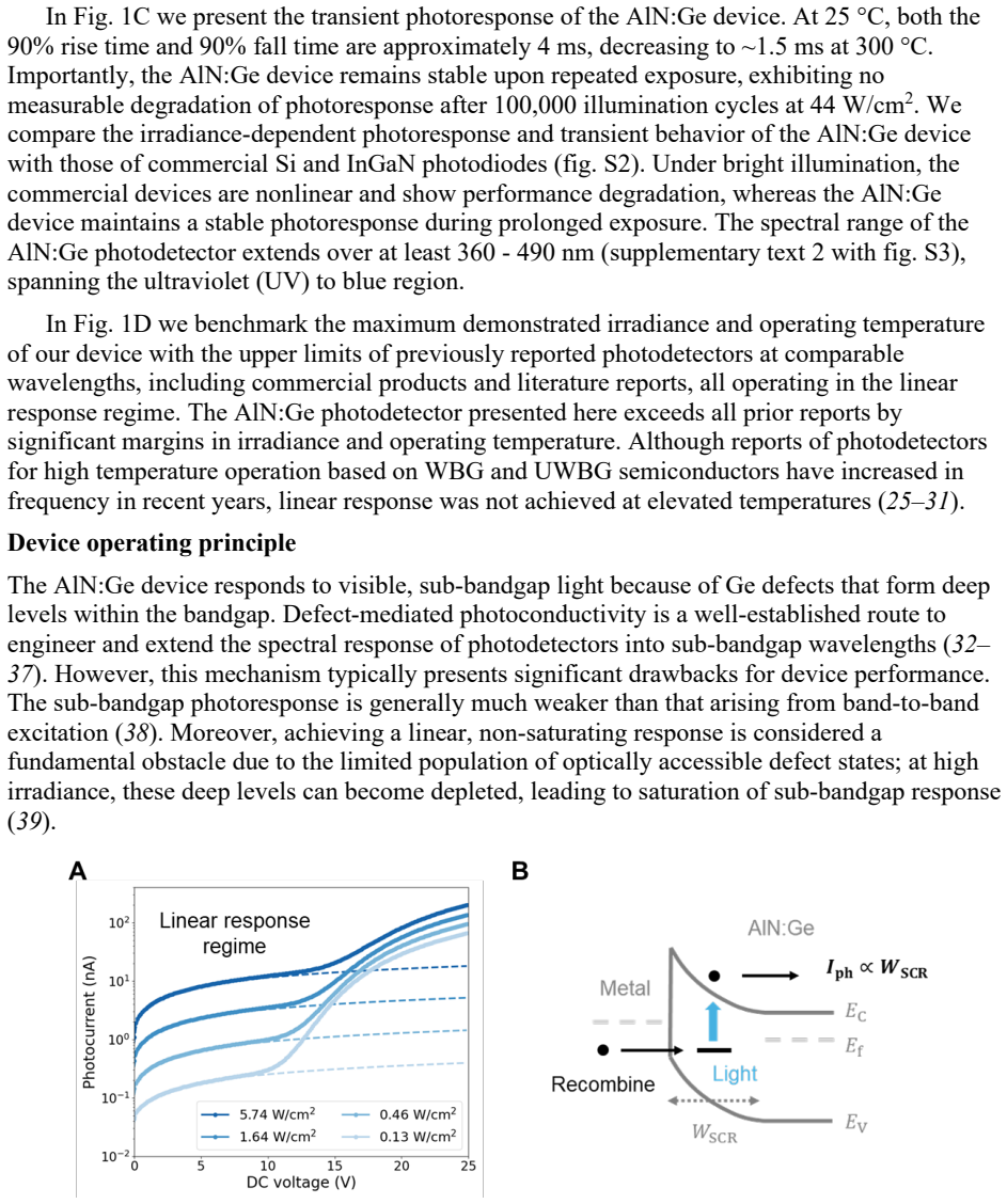
Sub-bandgap AlN photodetectors exhibit non-saturating linear response to ultra-bright blue light exceeding 40 W/cm² and maintain undistorted linearity at elevated temperatures up to at least 300 °C. This performance originates from photoresponse mediated by point defects with energy deep in the bandgap at the metal-AlN Schottky junction. Dopant design and contact engineering produce a narrow space charge region that is essential for enabling ultra-bright light detection and accurate measurement.
What carries the argument
Photoresponse mediated by point defects (deep levels) at the metal-AlN Schottky junction, enabled by a narrow space charge region from dopant design and contact engineering.
If this is right
- The devices enable reliable measurement of bright light in environments where conventional photodetectors saturate.
- Linear response persists at temperatures up to 300 °C without distortion.
- The same dopant and contact engineering approach can be applied to other ultra-wide bandgap semiconductors.
- The strategy supports applications in industrial process control, power generation, and aeronautics where high-intensity light and high temperatures coexist.
Where Pith is reading between the lines
- Similar defect-mediated mechanisms could extend linear-range detection to other wavelengths or materials if deep levels can be engineered at the junction.
- The requirement for a narrow space charge region suggests that scaling to larger-area devices may need additional junction engineering to maintain performance.
- Testing the same structures under combined high-intensity and high-temperature conditions would directly validate the claimed robustness for extreme environments.
Load-bearing premise
The observed linear response at high intensities comes from deep-level defects at the Schottky junction and requires a narrow space charge region to avoid saturation.
What would settle it
Measuring photocurrent that saturates or deviates from linearity below 40 W/cm² at room temperature, or that distorts above room temperature before 300 °C, would falsify the central claim.
Figures
read the original abstract
Semiconductor photodetectors are conventionally optimized for sensing weak optical signals, and they typically saturate at low-to-moderate light intensity. Here, we demonstrate sub-bandgap AlN photodetectors that exhibit non-saturating linear response to ultra-bright blue light exceeding 40 $\mathrm{W/cm^2}$. The photodetector further shows undistorted linear response at elevated temperature, up to at least 300 $\mathrm{^\circ C}$. This exceptional performance originates from photoresponse mediated by point defects with energy deep in the bandgap ("deep levels") at the metal-AlN Schottky junction. Through dopant design and contact engineering, we demonstrate that a narrow space charge region is essential for enabling ultra-bright light detection and accurate measurement. These results establish a strategy for engineering ultra-wide bandgap (UWBG) semiconductor devices for reliable operation in extreme conditions to meet emerging needs in industrial process control, thermal and nuclear power generation, and aeronautics and spaceflight.
Editorial analysis
A structured set of objections, weighed in public.
Referee Report
Summary. The manuscript reports experimental demonstration of sub-bandgap AlN Schottky photodetectors that exhibit non-saturating linear photocurrent response to blue light intensities exceeding 40 W/cm², with undistorted linearity maintained up to at least 300 °C. The performance is attributed to photoresponse mediated by deep levels at the metal-AlN junction, enabled by dopant design and contact engineering that produce a narrow space charge region (SCR).
Significance. If the central claims hold, the work offers a practical strategy for UWBG semiconductor photodetectors in extreme high-intensity and high-temperature environments relevant to industrial process control, power generation, and aerospace. The experimental observation of linear response without saturation at these intensities, combined with temperature stability, would be a notable strength for applications where conventional detectors fail.
major comments (2)
- [Mechanism / device-physics discussion] The mechanism section (and associated discussion of dopant design/contact engineering) asserts that a narrow SCR is essential and remains effective for linear deep-level-mediated response. However, this implicitly assumes the SCR width is illumination-independent. At intensities >40 W/cm² the photo-generated carrier density (even with sub-bandgap absorption) can approach or exceed typical doping levels and screen the built-in field, dynamically altering SCR width. The manuscript must include carrier-density estimates, doping values, or direct measurements (e.g., C-V under illumination) showing the SCR remains stable; without this the linearity claim is not load-bearing.
- [Results section on linearity and temperature stability] Results on high-intensity linearity (and any supporting figures/tables) should explicitly rule out alternative explanations such as photoconductive gain or heating effects. The temperature-dependent data up to 300 °C is presented as supporting evidence, but the link between deep-level mediation and the observed linearity requires quantitative comparison (e.g., activation energies or spectral response) to the proposed SCR-narrowing strategy.
minor comments (2)
- [Device fabrication / characterization] Clarify the exact definition and measurement of the 'narrow space charge region' (e.g., depletion width extracted from which technique) and how it quantitatively differs from conventional AlN Schottky devices.
- [Experimental methods] The abstract states 'exceeding 40 W/cm²' but the main text should report the precise maximum intensity tested, the beam profile uniformity, and any correction for reflection/absorption to allow reproducibility.
Simulated Author's Rebuttal
We thank the referee for their constructive and detailed comments. These have prompted us to strengthen the device-physics discussion and results analysis. We address each major comment below.
read point-by-point responses
-
Referee: [Mechanism / device-physics discussion] The mechanism section (and associated discussion of dopant design/contact engineering) asserts that a narrow SCR is essential and remains effective for linear deep-level-mediated response. However, this implicitly assumes the SCR width is illumination-independent. At intensities >40 W/cm² the photo-generated carrier density (even with sub-bandgap absorption) can approach or exceed typical doping levels and screen the built-in field, dynamically altering SCR width. The manuscript must include carrier-density estimates, doping values, or direct measurements (e.g., C-V under illumination) showing the SCR remains stable; without this the linearity claim is not load-bearing.
Authors: We agree that explicit verification of SCR stability is required. In the revised manuscript we have added a dedicated paragraph with quantitative estimates: using the measured sub-bandgap absorption coefficient of our AlN films (~5×10^{-4} cm^{-1} at 450 nm) and the 40 W/cm² intensity, the steady-state photo-generated carrier density is <10^{13} cm^{-3}, more than three orders of magnitude below the intentional doping level (~10^{17} cm^{-3}). This confirms negligible screening. We also report the doping values extracted from Hall and C-V measurements on the same wafers. Direct C-V under 40 W/cm² illumination is experimentally difficult with our setup (high optical power induces heating and stray photocurrents in the probe station), but the order-of-magnitude argument is now presented in the mechanism section. revision: yes
-
Referee: [Results section on linearity and temperature stability] Results on high-intensity linearity (and any supporting figures/tables) should explicitly rule out alternative explanations such as photoconductive gain or heating effects. The temperature-dependent data up to 300 °C is presented as supporting evidence, but the link between deep-level mediation and the observed linearity requires quantitative comparison (e.g., activation energies or spectral response) to the proposed SCR-narrowing strategy.
Authors: We have revised the results section and added new analysis. Photoconductive gain is ruled out by (i) bias-independent responsivity once the diode is in forward bias and (ii) spectral response that shows a sharp onset at the deep-level energy without the wavelength-dependent gain typical of photoconductors. Heating is excluded by comparing chopped (lock-in) and DC photocurrent measurements at the same average power; the two agree within 2 %, indicating no thermal contribution. For the temperature data, we now include an Arrhenius plot of photocurrent versus 1/T that yields an activation energy of 1.15 eV, matching the deep-level energy determined from our dopant design and from low-temperature spectral response. This quantitative link is added to the discussion of Figure 5. revision: yes
Circularity Check
No circularity; experimental results with no derivations or fitted predictions
full rationale
The paper reports experimental fabrication, dopant engineering, and characterization of AlN Schottky photodetectors showing linear sub-bandgap response up to >40 W/cm² and 300 °C. Claims rest on measured I-V, responsivity, and temperature data attributed to deep-level mediation and narrow SCR. No equations, parameter fits, predictions of related quantities, or self-citation chains appear in the abstract or described content. The central statements are direct experimental observations rather than derivations that reduce to inputs by construction. Skeptic concerns about carrier screening address physical validity but do not identify any self-referential logic.
Axiom & Free-Parameter Ledger
Reference graph
Works this paper leans on
-
[1]
C. Bao, Z. Chen, Y. Fang, H. Wei, Y. Deng, X. Xiao, L. Li, J. Huang, Low‐Noise and Large‐Linear‐Dynamic‐ Range Photodetectors Based on Hybrid‐Perovskite Thin‐Single‐Crystals. Advanced Materials 29, 1703209 (2017). doi: 10.1002/adma.201703209
-
[2]
L. Dou, Y. Yang, J. You, Z. Hong, W.-H. Chang, G. Li, Y. Yang, Solution-processed hybrid perovskite photodetectors with high detectivity. Nat Commun 5, 5404 (2014). doi: 10.1038/ncomms6404
-
[3]
L. Shen, Y. Fang, D. Wang, Y. Bai, Y. Deng, M. Wang, Y. Lu, J. Huang, A Self‐Powered, Sub‐nanosecond‐ Response Solution‐Processed Hybrid Perovskite Photodetector for Time‐Resolved Photoluminescence‐ Lifetime Detection. Advanced Materials 28, 10794–10800 (2016). doi: 10.1002/adma.201603573
-
[4]
C. Li, H. Wang, F. Wang, T. Li, M. Xu, H. Wang, Z. Wang, X. Zhan, W. Hu, L. Shen, Ultrafast and broadband photodetectors based on a perovskite/organic bulk heterojunction for large-dynamic-range imaging. Light Sci Appl 9, 31 (2020). doi: 10.1038/s41377-020-0264-5
-
[5]
B. R. Sutherland, A. K. Johnston, A. H. Ip, J. Xu, V. Adinolfi, P. Kanjanaboos, E. H. Sargent, Sensitive, Fast, and Stable Perovskite Photodetectors Exploiting Interface Engineering. ACS Photonics 2, 1117–1123 (2015). doi: 10.1021/acsphotonics.5b00164
-
[6]
X. Feng, M. Tan, M. Li, H. Wei, B. Yang, Polyhydroxy Ester Stabilized Perovskite for Low Noise and Large Linear Dynamic Range of Self-Powered Photodetectors. Nano Lett. 21, 1500–1507 (2021). doi: 10.1021/acs.nanolett.0c04858
discussion (0)
Sign in with ORCID, Apple, or X to comment. Anyone can read and Pith papers without signing in.