Phase Formation and Thermal Stability of Superconducting Platinum Silicide Thin Films on Silicon
Pith reviewed 2026-06-27 20:05 UTC · model grok-4.3
The pith
Phase-pure PtSi thin films form on silicon within minutes at 600 °C by rapid thermal processing and remain stable under extended annealing.
A machine-rendered reading of the paper's core claim, the machinery that carries it, and where it could break.
Core claim
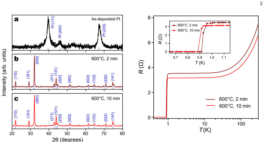
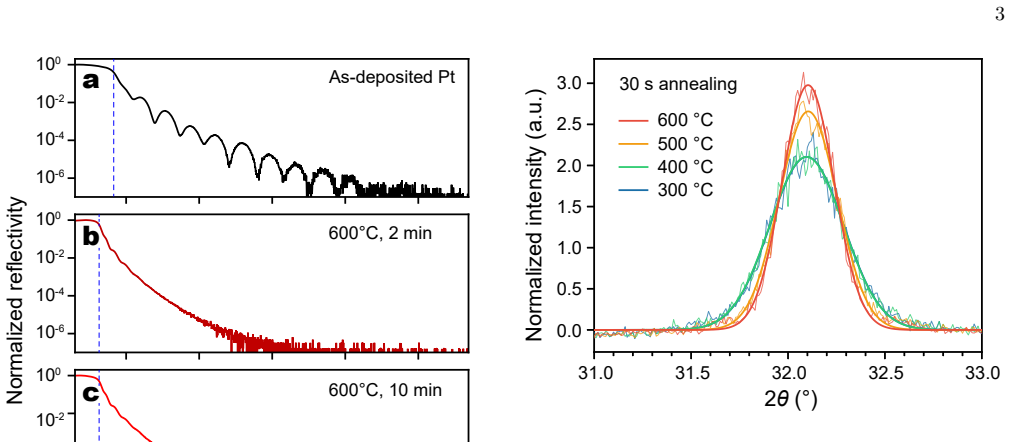
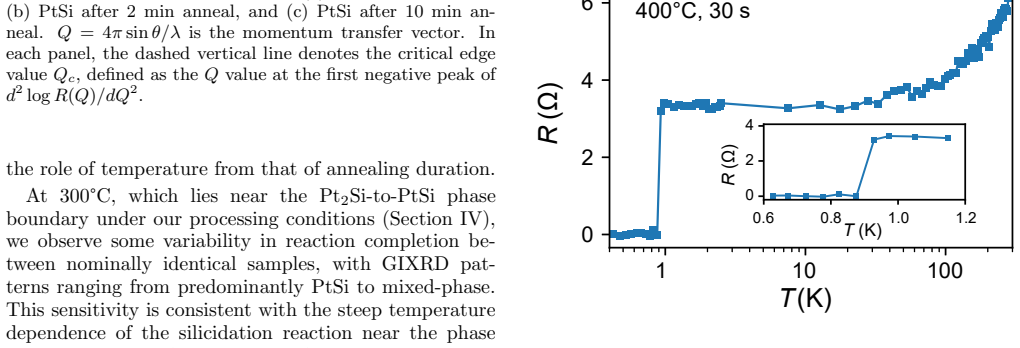
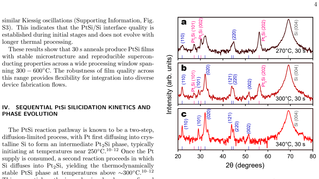
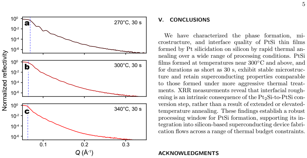
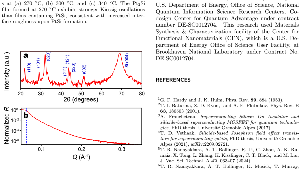
Phase-pure PtSi forms within minutes by rapid thermal processing at 600 °C and is stable under extended annealing, while 30 s anneals across 300-600 °C yield equivalent film quality with consistent microstructure and superconducting properties. X-ray reflectivity reveals that interfacial roughening is an intrinsic consequence of the Pt2Si-to-PtSi conversion step rather than a result of elevated temperature or prolonged annealing.
What carries the argument
The Pt2Si-to-PtSi phase conversion during rapid thermal annealing on silicon.
Load-bearing premise
Properties measured on test films by diffraction, reflectivity, and transport will translate directly to functional performance in full silicon-based superconducting quantum device stacks.
What would settle it
Observation of degraded superconducting transition temperature, excess interface scattering, or new defects in actual quantum device structures made with the reported PtSi process.
Figures
read the original abstract
Platinum silicide (PtSi) thin films are promising for silicon-based superconducting quantum devices due to their compatibility with CMOS fabrication, air stability, and superconducting transition temperature near 1 K. We report a systematic study of PtSi phase formation, microstructure, and interface quality as a function of annealing temperature and duration, characterizing films using grazing-incidence X-ray diffraction, X-ray reflectivity, and electrical transport measurements. Phase-pure PtSi forms within minutes by rapid thermal processing at 600 {\deg}C and is stable under extended annealing, while 30 s anneals across 300-600 {\deg}C yield equivalent film quality with consistent microstructure and superconducting properties. X-ray reflectivity reveals that interfacial roughening is an intrinsic consequence of the Pt2Si-to-PtSi conversion step rather than a result of elevated temperature or prolonged annealing. These results establish a robust processing window for PtSi formation in silicon-based superconducting device fabrication flows.
Editorial analysis
A structured set of objections, weighed in public.
Referee Report
Summary. The manuscript presents an experimental study of platinum silicide thin-film formation on silicon using rapid thermal processing. It claims that phase-pure PtSi forms within minutes at 600 °C, remains stable under extended annealing, and that 30 s anneals between 300–600 °C produce equivalent film quality, microstructure, and superconducting properties as measured by GIXRD, XRR, and electrical transport. The work further asserts that interfacial roughening observed by XRR is an intrinsic consequence of the Pt2Si-to-PtSi conversion step rather than a function of temperature or time, and concludes that these results establish a robust processing window for PtSi in silicon-based superconducting quantum device fabrication flows.
Significance. If the reported processing conditions and intrinsic-roughening conclusion hold, the results would supply concrete, CMOS-compatible guidelines for forming superconducting PtSi films with consistent Tc near 1 K, which could accelerate integration of silicide-based elements into silicon quantum circuits.
major comments (2)
- [Abstract, §4] Abstract and §4 (Conclusions): the central claim that the reported RTP conditions 'establish a robust processing window for PtSi formation in silicon-based superconducting device fabrication flows' extrapolates beyond the data. All GIXRD, XRR, and transport results are obtained on blanket Pt/Si test structures; no measurements on patterned devices, Josephson junctions, resonators, or multilayer stacks containing dielectrics or gates are presented. This gap directly undermines the device-fabrication claim.
- [§3.3] §3.3 (XRR analysis): the assertion that interfacial roughening is 'intrinsic' to the Pt2Si → PtSi conversion is supported only by comparing a limited set of blanket-film samples. Without quantitative error bars on the extracted roughness values or a control series that isolates conversion from other process variables, the 'intrinsic' interpretation remains under-constrained.
minor comments (2)
- [Abstract] The abstract states conclusions from GIXRD, XRR, and transport but contains no numerical values, error bars, or sample statistics; these should be added or the abstract shortened to avoid overstatement.
- [Figures] Figure captions and axis labels should explicitly state the number of samples measured and the fitting model used for XRR roughness extraction.
Simulated Author's Rebuttal
We thank the referee for the constructive feedback. We agree that the original manuscript overstated the direct applicability to full device fabrication flows and that the 'intrinsic' interpretation of interfacial roughening would benefit from additional quantification. We have revised the abstract, §4, and §3.3 accordingly while preserving the core experimental findings on blanket films.
read point-by-point responses
-
Referee: [Abstract, §4] Abstract and §4 (Conclusions): the central claim that the reported RTP conditions 'establish a robust processing window for PtSi formation in silicon-based superconducting device fabrication flows' extrapolates beyond the data. All GIXRD, XRR, and transport results are obtained on blanket Pt/Si test structures; no measurements on patterned devices, Josephson junctions, resonators, or multilayer stacks containing dielectrics or gates are presented. This gap directly undermines the device-fabrication claim.
Authors: We agree that the original wording in the abstract and conclusions extrapolates beyond the presented data, which are limited to blanket Pt/Si test structures. We have revised the abstract and §4 to state that the results establish a robust processing window for phase-pure PtSi formation on silicon substrates, providing a foundation for potential integration into silicon-based superconducting device flows. We have added explicit language noting that direct validation on patterned devices and multilayer stacks remains future work. revision: yes
-
Referee: [§3.3] §3.3 (XRR analysis): the assertion that interfacial roughening is 'intrinsic' to the Pt2Si → PtSi conversion is supported only by comparing a limited set of blanket-film samples. Without quantitative error bars on the extracted roughness values or a control series that isolates conversion from other process variables, the 'intrinsic' interpretation remains under-constrained.
Authors: We acknowledge that the original presentation lacked quantitative error bars and a fully isolating control series. The XRR trends show roughening coinciding specifically with the Pt2Si-to-PtSi conversion across multiple temperatures and times. In the revision we have added error bars to all extracted roughness values, expanded the discussion of the control experiments performed, and softened the wording from 'intrinsic' to 'consistent with an intrinsic consequence of the phase conversion step' while retaining the supporting data. revision: partial
Circularity Check
No circularity; purely experimental observations with no derivations or self-referential fits
full rationale
The paper reports direct experimental results from GIXRD phase identification, XRR roughness measurements, and transport Tc on Pt/Si blanket films under varying RTP conditions. No equations, derivations, fitted parameters, or mathematical predictions appear in the text. Claims about phase purity, stability, and intrinsic roughening are interpretations of measured data rather than reductions to inputs by construction. No self-citation chains or ansatzes are invoked to justify any derivation. The extrapolation concern raised by the skeptic is a question of external validity for device integration, not circularity in the reported chain.
Axiom & Free-Parameter Ledger
Reference graph
Works this paper leans on
-
[1]
and Bollinger, Anthony T
Nanayakkara, Tharanga R. and Bollinger, Anthony T. and Li, Ruoshui and Zhou, Chenyu and Rumaiz, Abdul K. and Tong, Xiao and Zhang, Lihua and Kisslinger, Kim and Black, Charles T. and Liu, Mingzhao , title =. J. Vac. Sci. Technol. A , volume =. 2024 , doi =
2024
-
[2]
and Bollinger, Anthony T
Nanayakkara, Tharanga R. and Bollinger, Anthony T. and Musick, Kevin and Murray, Thomas and Bhatia, Ekta and. Current-Phase Relations of Superconducting. Nano Lett. , volume =. 2026 , doi =
2026
-
[3]
and Hulm, John K
Hardy, George F. and Hulm, John K. , title =. Phys. Rev. , volume =. 1953 , doi =
1953
-
[4]
and Takaoka, S
Oto, K. and Takaoka, S. and Murase, K. and Ishida, S. , title =. J. Appl. Phys. , volume =. 1994 , doi =
1994
-
[5]
Baturina, T. I. and Kvon, Z. D. and Plotnikov, A. E. , title =. Phys. Rev. B , volume =. 2001 , doi =
2001
-
[6]
and Mazin, B
Szypryt, P. and Mazin, B. A. and Ulbricht, G. and Bumble, B. and Meeker, S. R. and Bockstiegel, C. and Walter, A. B. , title =. Appl. Phys. Lett. , volume =. 2016 , doi =
2016
-
[7]
Yao, Yao and Fernandes, Daniel F. and Ko. Self-aligned formation of superconducting sub-5 nm. APL Quantum , volume =. 2024 , doi =
2024
-
[8]
Superconducting Silicon On Insulator and silicide-based superconducting
Francheteau, Ana\". Superconducting Silicon On Insulator and silicide-based superconducting. 2017 , type =
2017
- [9]
-
[10]
and Schupp, F
Tsoukalas, K. and Schupp, F. and Sommer, L. and Bouquet, I. and Mergenthaler, M. and Paredes, S. and. Prospects of silicide contacts for silicon quantum electronic devices , journal =. 2024 , doi =
2024
-
[11]
and Gr\"
Stark, T. and Gr\". Deriving the kinetic parameters for. Thin Solid Films , volume =. 2000 , doi =
2000
-
[12]
Pant, A. K. and Murarka, S. P. and Shepard, C. and Lanford, W. , title =. J. Appl. Phys. , volume =. 1992 , doi =
1992
-
[13]
and Dubois, E
Larrieu, G. and Dubois, E. and Wallart, X. and Baie, X. and Katcki, J. , title =. J. Appl. Phys. , volume =. 2003 , doi =
2003
-
[14]
Naem, A. A. , title =. J. Appl. Phys. , volume =. 1988 , doi =
1988
-
[15]
and Schmid, P
Conforto, E. and Schmid, P. E. , title =. Philos. Mag. A , volume =. 2001 , doi =
2001
-
[16]
Vacuum , volume =
Shi, Mao-Lin and Xu, Jing and Dai, Ya-Wei and Cao, Qian and Chen, Lin and Sun, Qing-Qing and Zhou, Peng and Ding, Shi-Jin and Zhang, David Wei , title =. Vacuum , volume =. 2017 , doi =
2017
discussion (0)
Sign in with ORCID, Apple, or X to comment. Anyone can read and Pith papers without signing in.