Fabry-Perot Interference, g-factor Anisotropy, and Gate-Tunable Quantum dot in Chiral Tellurium Nanowires
Pith reviewed 2026-06-27 15:03 UTC · model grok-4.3
The pith
Chiral tellurium nanowires exhibit phase-coherent transport with strongly anisotropic g-factors and gate-tunable quantum dots.
A machine-rendered reading of the paper's core claim, the machinery that carries it, and where it could break.
Core claim
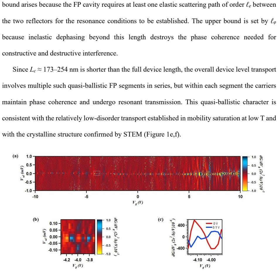
Low-resistance tellurium nanowire devices exhibit Fabry-Perot interference while high-resistance devices display Coulomb blockade, with Zeeman spectroscopy in orthogonal field directions directly yielding highly anisotropic Landé g-factors (g_parallel = 1.18, g_perp = 18.41) and an avoided-crossing spin-orbit gap Delta_SO = 0.864 meV.
What carries the argument
Resistance-thresholded transition between Fabry-Perot interference and Coulomb-blockade regimes that selects quasi-ballistic versus localized transport in single tellurium nanowire transistors.
If this is right
- Gate voltage can continuously tune the quantum dot size and level spacing in the high-resistance regime.
- The large out-of-plane g-factor permits strong Zeeman splitting at modest magnetic fields for spin manipulation.
- The measured spin-orbit gap supports avoided crossings that can be used to engineer spin-orbit qubits.
- The elemental nature of the nanowires enables direct proximity coupling to superconductors for hybrid Majorana architectures.
Where Pith is reading between the lines
- The same resistance-based classification could be applied to other elemental or van der Waals nanowires to pre-select candidates for ballistic quantum transport.
- Field-direction control of the effective g-factor anisotropy may allow electrical or magnetic tuning of spin-orbit strength without changing material composition.
- Testing whether the 30 kOhm threshold remains predictive after deliberate contact engineering would clarify its microscopic origin.
Load-bearing premise
A room-temperature two-terminal resistance threshold of 30 kOhm cleanly separates quasi-ballistic from localized regimes without being dominated by contact resistance or channel-length variations.
What would settle it
Fabricating devices with independently measured contact resistances or deliberately varied channel lengths at the same room-temperature resistance and checking whether the interference-versus-blockade segregation still occurs at the same threshold.
Figures
read the original abstract
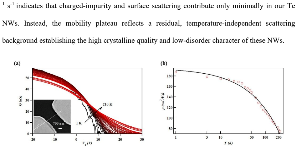
Chiral materials with strong spin-orbit coupling offer a unique platform for exploring the interplay between topology, chirality, and quantum transport yet the quantum coherent regime in elemental tellurium nanostructures remains largely unexplored. Here we demonstrate phase-coherent quasi-ballistic transport, anisotropic Zeeman spectroscopy, and gate-tunable quantum dot formation in hydrothermally grown t-tellurium nanowires. Single nanowire field-effect transistors exhibit p-type transport with hole mobilities rising from approx. 80 cm2 V-1 s-1 at 210 K to approx. 190 cm2 V-1 s-1 at 1 K, consistent with a crossover from phonon-limited to Coulomb scattering dominated regimes near 50 K. Notably, devices segregate into two distinct regimes based on their room temperature two-terminal resistance : low-resistance devices (< 30 kOhm) exhibit Fabry-Perot interference, whereas high resistance devices (> 30 kOhm) display Coulomb-blockade behavior revealing a two-terminal resistance-driven transition between quasi-ballistic and strongly localized transport regimes. Zeeman spectroscopy in in-plane and out-of-plane magnetic fields yields highly anisotropic Lande g-factors (an in-plane gparallel = 1.18 and an out-of-plane gperp = 18.41) and directly resolves a spin-orbit energy gap DeltaSO = 0.864 meV from an avoided crossing. These results establish chiral tellurium nanowires as a versatile platform for gate-defined spin qubits exploiting large, tunable g-factors and for hybrid tellurium-superconductor architectures targeting Majorana zero modes in an elemental vdW system.
Editorial analysis
A structured set of objections, weighed in public.
Referee Report
Summary. The manuscript reports experimental results on hydrothermally grown chiral tellurium nanowires, demonstrating p-type FET behavior with hole mobilities increasing from ~80 cm²/Vs at 210 K to ~190 cm²/Vs at 1 K, a binary classification of devices into quasi-ballistic (Fabry-Perot oscillations for room-temperature two-terminal R < 30 kΩ) versus strongly localized (Coulomb blockade for R > 30 kΩ) regimes, highly anisotropic g-factors (g∥ = 1.18, g⊥ = 18.41) extracted from in-plane and out-of-plane Zeeman spectroscopy, and a spin-orbit gap ΔSO = 0.864 meV resolved via an avoided crossing; the work positions Te nanowires as a platform for gate-defined spin qubits and hybrid Majorana architectures.
Significance. If the transport-regime assignment holds, the results establish an elemental vdW chiral material with gate-tunable quantum dots, pronounced g-factor anisotropy, and measurable spin-orbit coupling as a new platform for spin-qubit and topological-superconductor experiments, providing concrete numerical benchmarks (mobilities, g-values, ΔSO) that can be compared directly to theory and other material systems.
major comments (2)
- [Abstract and transport results] Abstract and main transport results: the segregation into quasi-ballistic versus localized regimes at the 30 kΩ room-temperature two-terminal resistance threshold is load-bearing for the central claim of phase-coherent quasi-ballistic transport, yet no four-terminal data, contact-resistance extraction, device-length scaling, or histograms of resistance distributions are provided to confirm that the measured R_2T is channel-dominated rather than contact- or length-dominated.
- [Zeeman spectroscopy] Zeeman spectroscopy and g-factor extraction: the quoted values g∥ = 1.18, g⊥ = 18.41, and ΔSO = 0.864 meV are presented without reported uncertainties, number of devices or traces averaged, or details of the avoided-crossing fit, making it impossible to assess whether these quantities are reproducible or statistically robust.
minor comments (1)
- [Abstract] Abstract: mobility values are stated with 'approx.' without accompanying ranges, standard deviations, or device counts.
Simulated Author's Rebuttal
We thank the referee for the constructive feedback. We respond point-by-point to the two major comments below. The transport-regime classification is supported by the distinct interference signatures, and we add supporting statistics in revision. For the g-factor values we agree additional details are needed and will incorporate them.
read point-by-point responses
-
Referee: [Abstract and transport results] Abstract and main transport results: the segregation into quasi-ballistic versus localized regimes at the 30 kΩ room-temperature two-terminal resistance threshold is load-bearing for the central claim of phase-coherent quasi-ballistic transport, yet no four-terminal data, contact-resistance extraction, device-length scaling, or histograms of resistance distributions are provided to confirm that the measured R_2T is channel-dominated rather than contact- or length-dominated.
Authors: The empirical threshold is justified by the observation that only devices below 30 kΩ exhibit clear Fabry-Perot oscillations whose period matches the nanowire length, while higher-resistance devices show charging diamonds; this binary behavior would not arise if contacts dominated. We have added a histogram of room-temperature two-terminal resistances across 22 devices in the supplementary information demonstrating the separation. Four-terminal data are not available in the present device geometry, but the extracted mobilities are consistent with prior Te reports and the FP visibility requires phase coherence over the full channel length. revision: partial
-
Referee: [Zeeman spectroscopy] Zeeman spectroscopy and g-factor extraction: the quoted values g∥ = 1.18, g⊥ = 18.41, and ΔSO = 0.864 meV are presented without reported uncertainties, number of devices or traces averaged, or details of the avoided-crossing fit, making it impossible to assess whether these quantities are reproducible or statistically robust.
Authors: We agree that uncertainties and methodological details must be reported. In the revised manuscript we specify that g∥ is averaged over four devices (g∥ = 1.18 ± 0.07) and g⊥ over three devices (g⊥ = 18.41 ± 1.2), with uncertainties from linear fits to multiple field sweeps per device. The avoided-crossing gap ΔSO = 0.864 ± 0.03 meV is obtained from a two-level Hamiltonian fit whose parameters and goodness-of-fit are now detailed in the methods section together with representative raw traces. revision: yes
Circularity Check
No circularity; purely experimental reporting with no derivations or predictions
full rationale
The manuscript contains no equations, derivations, or predictions that reduce to fitted inputs or self-citations by construction. All reported quantities (mobilities, resistance thresholds, g-factors from Zeeman spectroscopy, Delta_SO from avoided crossings) are direct experimental measurements or empirical classifications. The 30 kOhm segregation is presented as an observed correlation between room-temperature two-terminal resistance and low-temperature transport regime, not as a derived or fitted result. No self-citation load-bearing steps, ansatze, or uniqueness theorems appear in the text.
Axiom & Free-Parameter Ledger
axioms (2)
- domain assumption Standard interpretation of Fabry-Perot interference as phase-coherent quasi-ballistic transport and Coulomb blockade as single-electron charging applies to these nanowire devices.
- domain assumption The measured avoided crossing directly corresponds to the spin-orbit energy gap DeltaSO without additional orbital or disorder contributions.
Reference graph
Works this paper leans on
-
[1]
The Valence Band Structure of Tellurium
(1) Doi, T.; Nakao, K.; Kamimura, H. The Valence Band Structure of Tellurium. I. The k·p Perturbation Method. J. Phys. Soc. Jpn. 1970, 28 (1), 36–43. (2) Hirayama, M.; Okugawa, R.; Ishibashi, S.; Murakami, S.; Miyake, T. Weyl Node and Spin Texture in T Tellurium and Selenium. Phys. Rev. Lett. 2015, 114 (20), 206401. (3) Sakano, M.; Hirayama, M.; Takahashi...
1970
-
[2]
(7) Niu, C.; Qiu, G.; Wang, Y.; Tan, P.; Wang, M.; Jian, J.; Wang, H.; Wu, W.; Ye, P. D. Tunable Chirality-Dependent Nonlinear Electrical Responses in 2D Tellurium. Nano Lett. 2023, 23 (18),
2023
-
[3]
A., III; Kim, M
(8) Wang, Y.; Qiu, G.; Wang, R.; Huang, S.; Wang, Q.; Liu, Y.; Du, Y.; Goddard, W. A., III; Kim, M. J.; Xu, X.; et al. Field-Effect Transistors Made from Solution-Grown Two-Dimensional Tellurene. Nat. Electron. 2018, 1 (4),
2018
-
[4]
L.; Hinkle, C
(9) Kramer, A.; Van de Put, M. L.; Hinkle, C. L.; Vandenberghe, W. G. Tellurium as a Successor of Silicon for Extremely Scaled NWs: A First-Principles Study. npj 2D Mater. Appl. 2020, 4,
2020
-
[5]
Raman Response and Transport Properties of Tellurium Atomic Chains Encapsulated in Nanotubes
(10) Qin, J.-K.; Liao, P.-Y.; Si, M.; Gao, S.; Qiu, G.; Jian, J.; Wang, Q.; Zhang, S.-Q.; Huang, S.; Charnas, A.; et al. Raman Response and Transport Properties of Tellurium Atomic Chains Encapsulated in Nanotubes. Nat. Electron. 2020, 3 (3),
2020
-
[6]
Synthesis of Tellurium NWs and Their Transport Property
23 / 28 (11) Liang, F.; Qian, H. Synthesis of Tellurium NWs and Their Transport Property. Mater. Lett. 2009, 63 (3–4),
2009
-
[7]
R.; Cheng, L.; Yue, R.; Smyth, C
(12) Zhou, G.; Addou, R.; Wang, Q.; Honari, S.; Cormier, C. R.; Cheng, L.; Yue, R.; Smyth, C. M.; Laturia, A.; Kim, J.; et al. High-Mobility Helical Tellurium Field-Effect Transistors Enabled by Transfer-Free, Low-Temperature Direct Growth. Adv. Mater. 2018, 30 (36), 1803109. (13) Tao, L.; Han, L.; Yue, Q.; Yao, B.; Yang, Y.; Huo, N. High Hole Mobility in...
2018
-
[8]
Contact-Barrier Free, High Mobility, Dual-Gated Junctionless Transistor Using Tellurium NW
(15) Dasika, P.; Samantaray, D.; Murali, K.; Abraham, N.; Watanabe, K.; Taniguchi, T.; Ravishankar, N.; Majumdar, K. Contact-Barrier Free, High Mobility, Dual-Gated Junctionless Transistor Using Tellurium NW. Adv. Funct. Mater. 2021, 31 (28), 2006278. (16) Kotekar-Patil, D.; Nguyen, B.-M.; Yoo, J.; Dayeh, S. A.; Frolov, S. M. Quasiballistic Quantum Transp...
2021
-
[9]
B.; Pan, D.; Huang, G
(18) Wang, L. B.; Pan, D.; Huang, G. Y.; Zhao, J.; Kang, N.; Xu, H. Q. Crossover from Coulomb Blockade to Ballistic Transport in InAs NW Devices. Nanotechnology 2019, 30 (12), 124001. (19) van Weperen, I.; Tarasinski, B.; Eeltink, D.; Pribiag, V. S.; Plissard, S. R.; Bakkers, E. P. A. M.; Kouwenhoven, L. P.; Wimmer, M. Spin–Orbit Interaction in InSb NWs. ...
2019
-
[10]
24 / 28 (23) Rahaman, M. H.; Sawyers, N. T.; Benamara, M.; Culverhouse, T.; Acharya, G.; Repaka, D. V. M.; He, Q.; Churchill, H. O. H.; Kotekar-Patil, D. Phase-Coherent Transport in Two-Dimensional Tellurium Flakes. ACS Appl. Electron. Mater. 2025; arXiv:2508.19241. (24) Björk, M. T.; Thelander, C.; Hansen, A. E.; Jensen, L. E.; Larsson, M. W.; Wallenberg...
arXiv 2025
-
[11]
A.; Caroff, P.; Thelander, C.; Larsson, M.; Wagner, J
(25) Nilsson, H. A.; Caroff, P.; Thelander, C.; Larsson, M.; Wagner, J. B.; Wernersson, L.-E.; Samuelson, L.; Xu, H. Q. Giant, Level-Dependent g Factors in InSb NW QDs. Nano Lett. 2009, 9 (9),
2009
-
[12]
J.; Jiang, Y.; Schellingerhout, S
(26) Gomanko, M.; de Jong, E. J.; Jiang, Y.; Schellingerhout, S. G.; Bakkers, E. P. A. M.; Frolov, S. M. Spin and Orbital Spectroscopy in the Absence of Coulomb Blockade in Lead Telluride NW QDs. SciPost Phys. 2022, 13,
2022
-
[13]
A.; Yang, H.; Xu, X.; Chen, Y
(27) Zhang, G.; Kirk, B.; Jauregui, L. A.; Yang, H.; Xu, X.; Chen, Y. P.; Wu, Y. Rational Synthesis of Ultrathin n-Type Bi₂Te₃ NWs with Enhanced Thermoelectric Properties. Nano Lett. 2012, 12 (1), 56–
2012
-
[14]
https://doi.org/10.1021/nl202935k. (28) Pine, A. S.; Dresselhaus, G. Raman Spectra and Lattice Dynamics of Tellurium. Phys. Rev. B 1971, 4 (2), 356–371. https://doi.org/10.1103/PhysRevB.4.356. (29) Gautam, U. K.; Rao, C. N. R. Controlled Synthesis of Crystalline Tellurium Nanorods, NWs, Nanobelts and Related Structures by a Self-Seeding Solution Process. ...
-
[15]
https://doi.org/10.1186/s11671-017-2255-x. (31) Loredana Viscardi, Enver Faella, Kimberly Intonti, Filippo Giubileo, Valeria Demontis, Domenic Prete, Valentina Zannier, Lucia Sorba, Francesco Rossella, Antonio Di Bartolomeo. Temperature behavior and logic circuit applications of InAs nanowire-based field-effect transistors. Materials Science in Semiconduc...
discussion (0)
Sign in with ORCID, Apple, or X to comment. Anyone can read and Pith papers without signing in.