Synthesis and Characterization of Atomically-Sharp Superconductor-Dielectric Interface
Pith reviewed 2026-06-27 15:28 UTC · model grok-4.3
The pith
Zirconium oxide layers on niobium can be grown with atomic sharpness and higher crystallinity to reduce interface defects in quantum devices.
A machine-rendered reading of the paper's core claim, the machinery that carries it, and where it could break.
Core claim
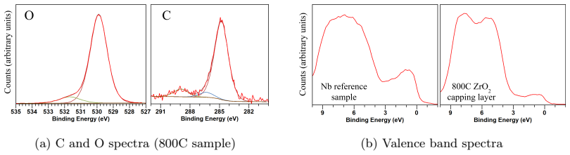
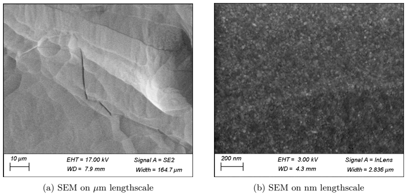
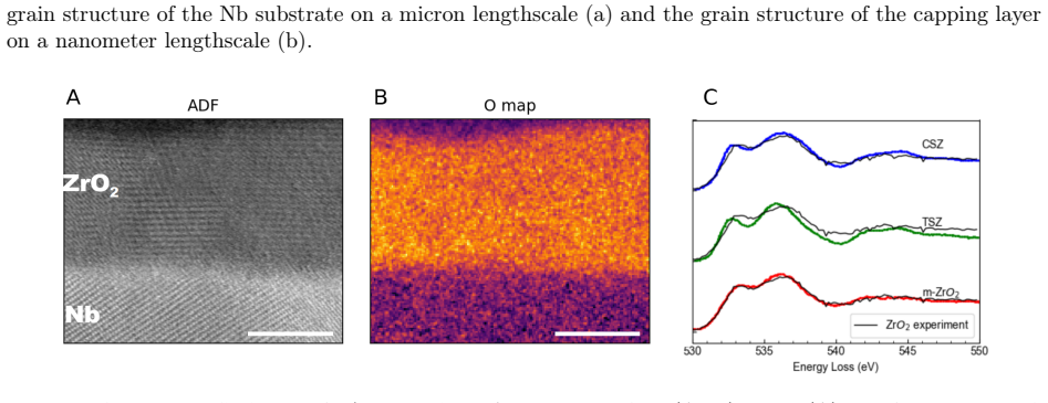
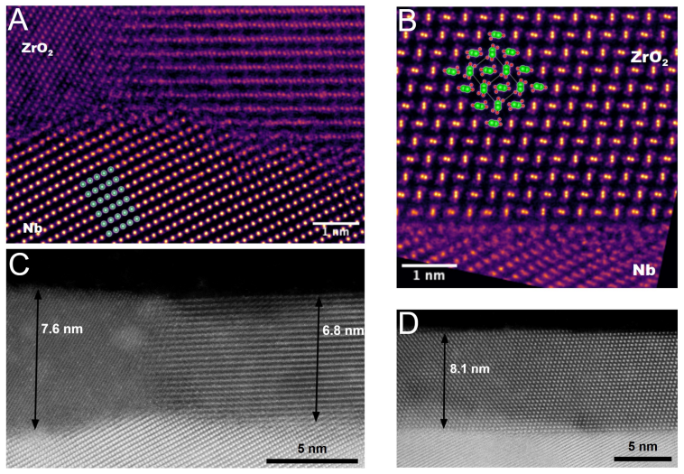
We explain the unique ability of zirconium oxide to form a crystalline layer, to maintain a sharp interface with metallic niobium, and to prevent niobium oxide re-growth in terms of the chemical properties of ZrO2 and the Nb-Zr-O ternary system. We demonstrate a new method to grow air-stable zirconium oxide layers on niobium with a higher level of crystallinity and a sharper oxide-metal interface than previously shown, and provide the first comprehensive microscopic analysis of ZrO2 capping layer properties.
What carries the argument
The ZrO2 capping layer on niobium, whose crystalline order and chemical stability within the Nb-Zr-O system produce an atomically sharp, air-stable barrier.
If this is right
- The new growth method produces ZrO2 layers with measurably higher crystallinity than earlier zirconium oxide films on niobium.
- The oxide-metal boundary remains atomically sharp without re-formation of niobium oxide even after air exposure.
- The crystalline barrier lowers the concentration of two-level system defects at the superconductor-dielectric interface.
- Air-stable layers simplify device fabrication while preserving low-loss properties.
Where Pith is reading between the lines
- The same growth chemistry might be tested on other superconductors such as aluminum to determine whether the Nb-Zr-O advantage generalizes.
- Direct comparison of coherence times in qubits made with these layers versus standard interfaces would test the defect-reduction claim.
- The microscopic analysis methods used here could be applied to evaluate other candidate crystalline barriers.
Load-bearing premise
That the crystalline structure and sharp interface of the zirconium oxide layer are what lower two-level system defect density and therefore reduce dissipation.
What would settle it
Fabrication of test resonators or qubits using the new ZrO2 layers that shows no measurable increase in quality factor or coherence time relative to devices using native niobium oxide.
Figures
read the original abstract
Modification of superconductor-dielectric interfaces is known to strongly impact coherence times of superconducting quantum devices. This relationship is thought to arise from differences in the concentration of "two-level system" defects in the disordered dielectrics and superconductor-dielectric interfaces; these defects couple to electromagnetic modes in the device and cause dissipation. Zirconium oxide barrier layers on niobium have emerged as a promising pathway to low-loss interfaces in recent years, evidently due to the crystalline nature of these layers in comparison to the amorphous niobium native oxide. We explain the unique ability of zirconium oxide to form a crystalline layer, to maintain a sharp interface with metallic niobium, and to prevent niobium oxide re-growth in terms of the chemical properties of ZrO$_2$ and the Nb-Zr-O ternary system. We demonstrate a new method to grow air-stable zirconium oxide layers on niobium with a higher level of crystallinity and a sharper oxide-metal interface than previously shown, and provide the first comprehensive microscopic analysis of ZrO$_2$ capping layer properties. These developments pave the way toward vital performance advances in superconducting quantum devices.
Editorial analysis
A structured set of objections, weighed in public.
Referee Report
Summary. The manuscript claims to demonstrate a new synthesis method for air-stable crystalline ZrO2 layers on Nb that achieves higher crystallinity and an atomically sharper oxide-metal interface than prior work. It attributes this capability to the chemical properties of ZrO2 and the Nb-Zr-O ternary system, provides what is described as the first comprehensive microscopic analysis of the capping layer, and positions the result as a route to reduced two-level system defects and improved coherence in superconducting quantum devices.
Significance. If the synthesis method and characterization data substantiate the claims of improved crystallinity and interface sharpness, the work could offer a useful materials advance for superconductor-dielectric interfaces in quantum devices. The chemical rationale and microscopic analysis would add value to interface engineering literature. However, the absence of any direct dielectric-loss, resonator, or qubit measurements means the asserted benefit for TLS reduction and device performance remains an untested premise rather than a demonstrated outcome.
major comments (2)
- [Abstract] Abstract and provided text: the central experimental claims of higher crystallinity, sharper interfaces, and comprehensive microscopic analysis are asserted without any supporting data, methods details, figures, or quantitative metrics in the manuscript as presented; this prevents evaluation of whether the new method actually delivers the stated improvements.
- [Abstract] The motivation explicitly links crystalline ZrO2 to lower TLS dissipation versus amorphous NbOx, yet no resonator, qubit, or dielectric-loss measurements are reported to test this link; the TLS-reduction benefit is therefore an assumption rather than a result.
Simulated Author's Rebuttal
We thank the referee for the detailed review and constructive feedback. We address the major comments point by point below.
read point-by-point responses
-
Referee: [Abstract] Abstract and provided text: the central experimental claims of higher crystallinity, sharper interfaces, and comprehensive microscopic analysis are asserted without any supporting data, methods details, figures, or quantitative metrics in the manuscript as presented; this prevents evaluation of whether the new method actually delivers the stated improvements.
Authors: The manuscript contains dedicated sections on experimental methods, results with supporting figures (including XRD, TEM, and interface analysis), and quantitative metrics such as crystallinity indicators and interface width measurements. The abstract serves as a summary of these findings. If the reviewed version appeared to lack these elements, we will ensure clearer cross-references and prominence in the revised manuscript. revision: partial
-
Referee: [Abstract] The motivation explicitly links crystalline ZrO2 to lower TLS dissipation versus amorphous NbOx, yet no resonator, qubit, or dielectric-loss measurements are reported to test this link; the TLS-reduction benefit is therefore an assumption rather than a result.
Authors: We agree that the manuscript reports no direct dielectric-loss, resonator, or qubit measurements, as its scope is limited to synthesis and microscopic characterization of the ZrO2/Nb interface. The TLS benefit is discussed as motivation drawn from prior literature on crystalline versus amorphous oxides and is framed as enabling future advances rather than a demonstrated outcome here. We will revise the abstract and discussion sections to make this distinction explicit. revision: yes
Circularity Check
No circularity: experimental synthesis/characterization paper with no derivations or fitted predictions
full rationale
This is a purely experimental materials paper reporting a growth method for ZrO2 on Nb, supported by microscopic analysis (TEM, etc.) and chemical explanations of the Nb-Zr-O system. No equations, no first-principles derivations, no parameters fitted to data then re-presented as predictions, and no self-citation chains invoked to justify uniqueness theorems or ansatzes. The TLS-dissipation motivation is stated as background and remains an untested premise rather than a derived claim inside the paper. All central results rest on direct synthesis and characterization evidence external to any internal fitting or self-reference.
Axiom & Free-Parameter Ledger
axioms (1)
- domain assumption Crystalline ZrO2 layers reduce two-level system defect concentration relative to amorphous Nb native oxide, leading to lower dissipation.
Reference graph
Works this paper leans on
-
[1]
I.; Dhuley, R
Hollister, M. I.; Dhuley, R. C.; Tatkowski, G. L. A large millikelvin platform at Fermilab for quantum computing applications. IOP Conference Series: Materials Science and Engineering. 2022; p 012045
2022
-
[2]
Romanenko, A.; Pilipenko, R.; Zorzetti, S.; Frolov, D.; Awida, M.; Belomestnykh, S.; Posen, S.; Gras- sellino, A.Physical Review Applied2020,13, 034032
-
[3]
M.; Chausovsky, D.; Kahn, N.; Curek, E.; Lafont, F.; Rosenblum, S.PRX Quantum2023,4, 030336
Milul, O.; Guttel, B.; Goldblatt, U.; Hazanov, S.; Joshi, L. M.; Chausovsky, D.; Kahn, N.; Curek, E.; Lafont, F.; Rosenblum, S.PRX Quantum2023,4, 030336
-
[4]
A.; Zhu, S.; Crisa, F.; You, X.; Huang, Z.; Roy, T.; Lee, J.; Zanten, D
Bal, M.; Murthy, A. A.; Zhu, S.; Crisa, F.; You, X.; Huang, Z.; Roy, T.; Lee, J.; Zanten, D. v.; Pilipenko, R.; othersnpj Quantum Information2024,10, 43
-
[5]
Siddiqi, I.Nature Reviews Materials2021,6, 875–891
-
[6]
L.; Girvin, S
Blais, A.; Grimsmo, A. L.; Girvin, S. M.; Wallraff, A.Reviews of Modern Physics2021,93, 025005
-
[7]
M.; Kustura, K.; Gonzalez-Ballestero, C.; Romero-Isart, O.; Kirchmair, G
Heidler, P.; Schneider, C. M.; Kustura, K.; Gonzalez-Ballestero, C.; Romero-Isart, O.; Kirchmair, G. Physical Review Applied2021,16, 034024
-
[8]
Kalboussi, Y.; Delatte, B.; Bira, S.; Dembele, K.; Li, X.; Miserque, F.; Brun, N.; Walls, M.; Maurice, J.- L.; Dragoe, D.; othersApplied Physics Letters2024,124
-
[9]
Kalboussi, Y.; Curci, I.; Miserque, F.; Troadec, D.; Brun, N.; Walls, M.; Jullien, G.; Eozenou, F.; Baudrier, M.; Maurice, L.; othersPhysical Review Applied2025,23, 044023
-
[10]
H.; Lisenfeld, J.Reports on Progress in Physics2019,82, 124501
Müller, C.; Cole, J. H.; Lisenfeld, J.Reports on Progress in Physics2019,82, 124501
-
[11]
D.; Ansmann, M.; Bialczak, R
O’Connell, A. D.; Ansmann, M.; Bialczak, R. C.; Hofheinz, M.; Katz, N.; Lucero, E.; McKenney, C.; Neeley, M.; Wang, H.; Weig, E. M.; othersApplied Physics Letters2008,92
-
[12]
Romanenko, A.; Schuster, D.Physical Review Letters2017,119, 264801
-
[13]
M.; Cooper, K
Martinis, J. M.; Cooper, K. B.; McDermott, R.; Steffen, M.; Ansmann, M.; Osborn, K.; Cicak, K.; Oh, S.; Pappas, D. P.; Simmonds, R. W.; othersPhysical review letters2005,95, 210503
-
[14]
O.; Butterling, M.; Stiehl, M.; Semione, G
Wenskat, M.; Čižek, J.; Liedke, M. O.; Butterling, M.; Stiehl, M.; Semione, G. D. L.; Backes, C.; Bate, C.; Melikhova, O.; Hirschmann, E.; othersPhysical Review B2022,106, 094516
-
[15]
Bafia, D.; Murthy, A.; Grassellino, A.; Romanenko, A.Physical Review Applied2024,22, 024035
-
[16]
P.; Griffith, K
Koçer, C. P.; Griffith, K. J.; Grey, C. P.; Morris, A. J.Physical Review B2019,99, 075151
-
[17]
Sitaraman, N. S. Theory work on SRF materials. Ph.D. thesis, Cornell University, 2022
2022
-
[18]
Nano hetero-structures for improving performances of superconductors under high fields
Kalboussi, Y. Nano hetero-structures for improving performances of superconductors under high fields. Ph.D. thesis, Université Paris-Saclay, 2023
2023
-
[19]
Sitaraman, N.; Gaitan, G.; Oseroff, T.; Baraissov, Z.; Sun, Z.; Muller, D.; Arias, T.; Liepe, M.2023,
2023
-
[20]
A.; Muller, D
Choi, J.; Olszewski, M.; Zhang, L.; Baraissov, Z.; Banerjee, T.; Aggarwal, K.; Chaudhari, S.; Arias, T. A.; Muller, D. A.; Fatemi, V.; othersAPL Materials2025,13. 12
-
[21]
21th International Conference on RF Superconductivity (SRF’23), Grand Rapids, MI, USA, 25-30 June
Kalboussi, Y.; Delatte, B.; Miserque, F.; Dragoe, D.; Asaduzzaman, M.; Maurice, L.; Baudrier, M.; Jullien,G.; Boulch,C.; Vacher,T.; othersSurfaceEngineeringbyALDforSuperconductingRFCavities. 21th International Conference on RF Superconductivity (SRF’23), Grand Rapids, MI, USA, 25-30 June
-
[22]
Crystallinity in niobium oxides: A pathway for mitigation of two-level-system defects in niobium 3D resonator for quantum applications
Proslier, T.; Kalboussi, Y.; Curci, I.; Jullien, G.; Eozenou, F.; Maurice, L.; Sahuquet, P. Crystallinity in niobium oxides: A pathway for mitigation of two-level-system defects in niobium 3D resonator for quantum applications. 22nd International Conference on RF Superconductivity (SRF’25), Tokyo, Japan, 21-26 September 2025. 2025
2025
-
[23]
Grassellino, A.; Romanenko, A.; Bice, D.; Melnychuk, O.; Crawford, A.; Chandrasekaran, S.; Sung, Z.; Sergatskov, D.; Checchin, M.; Posen, S.; othersarXiv preprint arXiv:1806.098242018,
-
[24]
Accel.1998,60, 103–120
Dacca, A.; Gemme, G.; Parodi, R.; Mattera, L.Part. Accel.1998,60, 103–120
1998
-
[25]
Lackner, P.; Zou, Z.; Mayr, S.; Diebold, U.; Schmid, M.Physical Chemistry Chemical Physics2019, 21, 17613–17620
-
[26]
Prudnikava, A.; Tamashevich, Y.; Makarova, A.; Smirnov, D.; Knobloch, J.Superconductor Science and Technology2024,37, 075007
-
[27]
E.; Ragazzon, D.; Borg, A.; Uvdal, P.; Skorodumova, N
Kamal, C.; Stenberg, N.; Walle, L. E.; Ragazzon, D.; Borg, A.; Uvdal, P.; Skorodumova, N. V.; Odelius, M.; Sandell, A.Physical Review Letters2021,126, 016102
-
[28]
Kerber, S.; Bruckner, J.; Wozniak, K.; Seal, S.; Hardcastle, S.; Barr, T.Journal of Vacuum Science & Technology A: Vacuum, Surfaces, and Films1996,14, 1314–1320
-
[29]
W.; Etourneau, J.; Subramanian, M.International Journal of Inor- ganic Materials2001,3, 1091–1094
Portier, J.; Campet, G.; Kwon, C. W.; Etourneau, J.; Subramanian, M.International Journal of Inor- ganic Materials2001,3, 1091–1094
-
[30]
Dimitrov, V.; Sakka, S.Journal of Applied Physics1996,79, 1736–1740
-
[31]
Zandiehnadem, F.; Murray, R.; Ching, W.Physica B+C1988,150, 19–24
-
[32]
Soriano, L.; Abbate, M.; Faber, J.; Morant, C.; Sanz, J.Solid State Communications1995,93, 659–665
-
[33]
W.Physical Review B1996,54, 7094
McComb, D. W.Physical Review B1996,54, 7094
-
[34]
H.; Duffy, J
Binks, J. H.; Duffy, J. A.J. Chem. Soc., Faraday Trans. 21985,81, 473–478
-
[35]
Dimitrov, V.; Komatsu, T.Journal of Solid State Chemistry2002,163, 100–112
-
[36]
Kuroda, Y.; Hamano, H.; Mori, T.; Yoshikawa, Y.; Nagao, M.Langmuir2000,16, 6937–6947
-
[37]
W.; TALLAN, N
VEST, R. W.; TALLAN, N. M.; TRIPP, W. C.Journal of the American Ceramic Society1964,47, 635–640
-
[38]
L.Journal of the American Chemical Society1954,76, 2651–2652
Hoch, M.; Nakata, M.; Johnston, H. L.Journal of the American Chemical Society1954,76, 2651–2652
-
[39]
Chase, M.NIST-JANAF Thermochemical Tables, 4th Edition; American Institute of Physics, 1998
1998
-
[40]
Fairley, N.; Fernandez, V.; Richard-Plouet, M.; Guillot-Deudon, C.; Walton, J.; Smith, E.; Flahaut, D.; Greiner, M.; Biesinger, M.; Tougaard, S.; othersApplied Surface Science Advances2021,5, 100112
-
[41]
Mårtensson, N.; Nyholm, R.Physical Review B1981,24, 7121
-
[42]
T.; Tate, M
Philipp, H. T.; Tate, M. W.; Shanks, K. S.; Mele, L.; Peemen, M.; Dona, P.; Hartong, R.; van Veen, G.; Shao, Y.-T.; Chen, Z.; othersMicroscopy and Microanalysis2022,28, 425–440
-
[43]
E.; Yoon, D.; Ma, D.; Muller, D
Lee, C.-H.; Zeltmann, S. E.; Yoon, D.; Ma, D.; Muller, D. A.Microscopy and Microanalysis2025,31, ozaf070. 13
discussion (0)
Sign in with ORCID, Apple, or X to comment. Anyone can read and Pith papers without signing in.