Structural Changes and Transport Properties of YBa₂Cu₃O₇ Locally Modified by a He^+ Focused Ion Beam
Pith reviewed 2026-06-27 08:05 UTC · model grok-4.3
The pith
Focused He+ ion beams expand the YBCO lattice and suppress Tc to create insulating regions for nano-devices.
A machine-rendered reading of the paper's core claim, the machinery that carries it, and where it could break.
Core claim
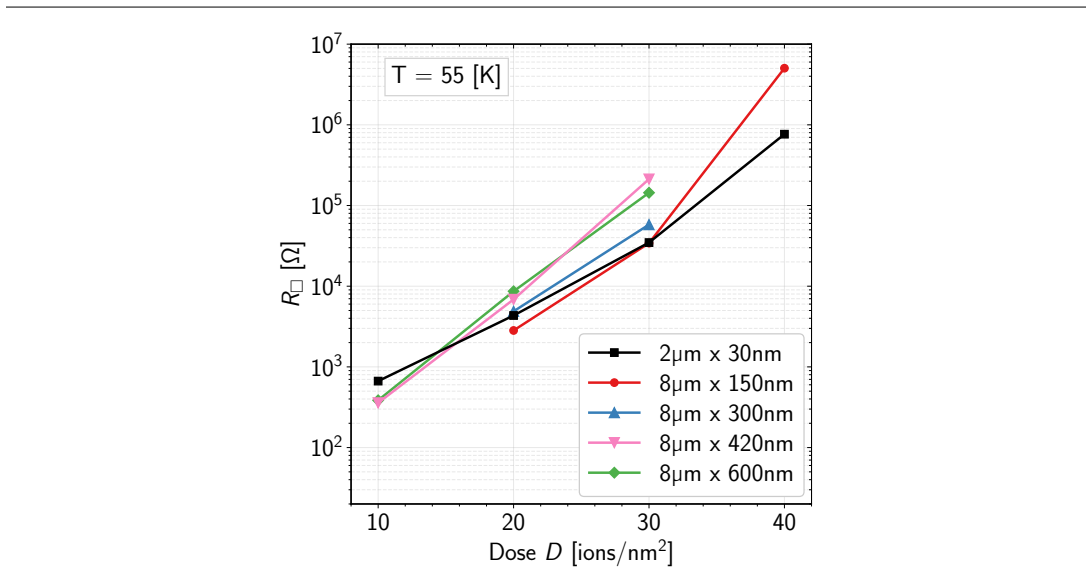
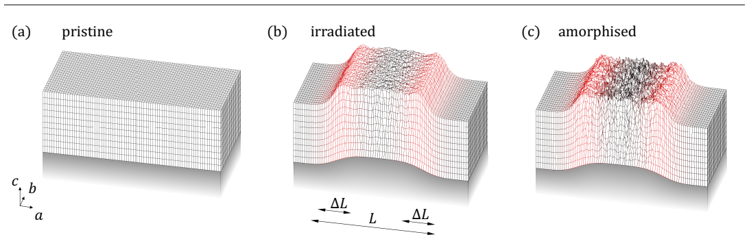
Irradiation of epitaxially grown YBa2Cu3O7 thin films with 30 keV He+ ions leads to expansion of the crystal lattice, decrease of the critical temperature Tc and eventually transition to an insulator. Fabrication of such insulating regions with a focused He-Ion beam with a spot size of ~10 nm is a powerful technique for fabrication of superconducting nano-devices.
What carries the argument
Dose-controlled 30 keV He+ focused ion beam irradiation that creates defects to drive lattice expansion and transport changes in YBCO.
If this is right
- Increasing dose produces a continuous transition from superconducting to fully insulating behavior.
- The modification remains effective at lateral dimensions as small as 30 nm.
- Nanofocused X-ray diffraction can resolve the local structural expansion inside individual irradiated spots.
- The approach supports direct writing of insulating barriers inside a single YBCO film for device structures.
Where Pith is reading between the lines
- Narrow insulating barriers written by the beam could form Josephson junctions between adjacent superconducting regions in the same film.
- The same dose window may produce comparable modifications in other cuprate films.
- Integration with standard lithography steps could produce hybrid circuits containing both superconducting and normal regions on one chip.
Load-bearing premise
The structural and transport changes are caused solely by ion-induced defects whose density is controlled by the stated dose.
What would settle it
Measurement of comparable lattice expansion or Tc reduction in regions never exposed to the ion beam, or absence of dose dependence across the 10-100 ions/nm2 range, would indicate other mechanisms dominate.
Figures
read the original abstract
Irradiation of a material with ions can cause various defects that can lead to structural phase transitions and the modification of the material's properties. Here we study the irradiation of the epitaxyally grown thin films of the high-temperature superconductor $\mathrm{YBa_2Cu_3O_7}$ with $30\,\mathrm{keV}$ He$^{+}$ ions which leads to the expansion of the crystal lattice, decrease of the critical temperature $T_c$ and eventually transition to an insulator. Fabrication of such insulating regions with a focused He-Ion beam with a spot size of $\sim 10\,\mathrm{nm}$ is a powerful technique for fabrication of superconducting nano-devices. Using low-temperature resistivity measurements, diffraction with a nanofocused X-ray beam and atomic force microscopy, we investigated how the structure and the electric transport properties of $\mathrm{YBa_2Cu_3O_7}$ depend on the irradiation dose in a range $10$--$100\,\mathrm{ions/nm^2}$ and on the lateral size of the irradiated area in a range $30$--$5000\,\mathrm{nm}$.
Editorial analysis
A structured set of objections, weighed in public.
Referee Report
Summary. The manuscript examines the effects of 30 keV He+ focused ion beam irradiation on epitaxially grown YBa2Cu3O7 thin films. It reports that doses in the range 10--100 ions/nm² produce lattice expansion, suppression of the critical temperature Tc, and a transition to an insulating state. Lateral sizes of irradiated regions are varied from 30 nm to 5000 nm and characterized via low-temperature resistivity, nanofocused X-ray diffraction, and atomic force microscopy. The authors conclude that the ~10 nm beam spot size makes this approach powerful for fabricating superconducting nano-devices by creating insulating regions.
Significance. If the dose-controlled structural and transport modifications can be reliably extended to the 10 nm scale without significant confounding contributions from heating, redeposition or substrate effects, the technique would provide a useful tool for patterning high-Tc superconducting nanostructures. The combination of transport and structural probes is a positive feature of the experimental design.
major comments (2)
- [Abstract] Abstract: the central claim that the ~10 nm spot size enables fabrication of superconducting nano-devices is not supported by the reported data, which only covers irradiated areas from 30 nm to 5000 nm. No measurements or analysis of edge/proximity effects below 30 nm are described, leaving the extrapolation to the claimed resolution unsecured.
- [Abstract] Abstract: the manuscript provides no quantitative values, error bars, or statistical details for the reported lattice expansion, Tc suppression, or resistivity changes, preventing assessment of the magnitude, reproducibility, and dose dependence of the effects.
minor comments (1)
- [Abstract] Typo: 'epitaxyally' should read 'epitaxially'.
Simulated Author's Rebuttal
We thank the referee for the constructive comments on our manuscript. We address the two major points below and will revise the abstract accordingly.
read point-by-point responses
-
Referee: [Abstract] Abstract: the central claim that the ~10 nm spot size enables fabrication of superconducting nano-devices is not supported by the reported data, which only covers irradiated areas from 30 nm to 5000 nm. No measurements or analysis of edge/proximity effects below 30 nm are described, leaving the extrapolation to the claimed resolution unsecured.
Authors: We agree that the abstract's phrasing extrapolates beyond the presented data. The experiments demonstrate dose-dependent modifications for irradiated regions as small as 30 nm, which is already relevant for nano-scale patterning given the ~10 nm beam spot size. However, we did not measure or analyze features below 30 nm or quantify edge/proximity effects at that scale. We will revise the abstract to state that the approach enables fabrication of insulating regions down to 30 nm lateral size, with the beam spot size indicating potential for further miniaturization, rather than claiming direct support for 10 nm devices. revision: yes
-
Referee: [Abstract] Abstract: the manuscript provides no quantitative values, error bars, or statistical details for the reported lattice expansion, Tc suppression, or resistivity changes, preventing assessment of the magnitude, reproducibility, and dose dependence of the effects.
Authors: The abstract summarizes the dose range and observed phenomena but does not include specific numerical values or uncertainties. We will revise the abstract to incorporate representative quantitative results (e.g., approximate lattice expansion percentages, Tc shifts, and resistivity changes at key doses) along with indications of reproducibility from the multiple measurements performed. revision: yes
Circularity Check
No circularity; purely experimental characterization with no derivations or self-referential predictions
full rationale
The manuscript reports direct experimental measurements (low-temperature resistivity, nanofocused X-ray diffraction, AFM) of dose- and size-dependent changes in lattice expansion, Tc, and insulation in irradiated YBa2Cu3O7 films. No equations, fitted parameters, predictive models, or derivation chains appear. The spot-size claim (~10 nm) is a statement of instrument capability, not a derived result. All load-bearing statements reduce to measured data rather than to self-citation chains or definitional identities. This is the expected outcome for a characterization study.
Axiom & Free-Parameter Ledger
Reference graph
Works this paper leans on
-
[1]
S. A. Cybart, E. Y. Cho, T. J. Wong, B. H. Wehlin, M. K. Ma, C. Huynh, R. C. Dynes, Nat. Nanotechnol. 2015, 10 598
2015
-
[2]
Weber, D
T. Weber, D. Jetter, J. Ullmann, S. A. Koch, S. F. Pfander, K. Kress, A. Vervelaki, B. Gross, O. Kieler, U. Drechsler, P. R. Baral, A. Magrez, R. Kleiner, A. W. Knoll, M. Poggio, D. Koelle, Phys. Rev. Appl. 2025, 24 054041
2025
-
[3]
Kasaei, T
L. Kasaei, T. Melbourne, V. Manichev, L. C. Feldman, T. Gustafsson, K. Chen, X. X. Xi, B. A. Davidson, AIP Adv. 2018, 8, 7 075020
2018
-
[4]
Kasaei, T
L. Kasaei, T. Melbourne, M. Li, V. Manichev, F. Qin, H. Hijazi, L. C. Feldman, T. Gustafsson, B. A. Davidson, X. Xi, K. Chen, IEEE Trans. Appl. Supercond. 2019, 29, 5 1
2019
-
[5]
D. Yin, X. Cai, T. Xu, R. Sun, Z. Chen, Y. Han, L. Tian, Y. Wang, Y. Zhang, Z. Gan, Phys. C 2024, 623 1354532
2024
-
[6]
Z. Chen, Y. Zhang, P. Ma, Z. Xu, Y. Li, Y. Wang, J. Lu, Y. Ma, Z. Gan, Chin. Phys. B 2024, 33, 4 047405
2024
-
[7]
Ruhtinas, I
A. Ruhtinas, I. J. Maasilta, Phys. Rev. Res. 2025, 7 043252
2025
-
[8]
Karrer, B
M. Karrer, B. Aichner, K. Wurster, C. Mag\'en, C. Schmid, R. Hutt, B. Budinsk\'a, O. V. Dobrovolskiy, R. Kleiner, W. Lang, E. Goldobin, D. Koelle, Phys. Rev. Appl. 2024, 22 014043
2024
-
[9]
Aichner, L
B. Aichner, L. Backmeister, M. Karrer, K. Wurster, R. Kleiner, E. Goldobin, D. Koelle, W. Lang, Condensed Matter 2023, 8, 2 32
2023
-
[10]
Backmeister, B
L. Backmeister, B. Aichner, M. Karrer, K. Wurster, R. Kleiner, E. Goldobin, D. Koelle, W. Lang, Nanomaterials 2022, 12, 19
2022
-
[11]
E. Y. Cho, Y. W. Zhou, J. Y. Cho, S. A. Cybart, Appl. Phys. Lett. 2018, 113, 2 022604
2018
-
[12]
uller, M. Karrer, F. Limberger, M. Becker, B. Schr\
B. M\"uller, M. Karrer, F. Limberger, M. Becker, B. Schr\"oppel, C. Burkhardt, R. Kleiner, E. Goldobin, D. Koelle, Phys. Rev. Appl. 2019, 11 044082
2019
-
[13]
Couëdo, P
F. Couëdo, P. Amari, C. Feuillet-Palma, C. Ulysse, Y. K. Srivastava, R. Singh, N. Bergeal, J. Lesueur, Sci. Rep. 2020, 10, 1 10256
2020
-
[14]
Z. Chen, Y. Li, R. Zhu, J. Xu, T. Xu, D. Yin, X. Cai, Y. Wang, J. Lu, Y. Zhang, P. Ma, Chin. Phys. Lett. 2022, 39, 7 077402
2022
-
[15]
E. Y. Cho, M. K. Ma, C. Huynh, K. Pratt, D. N. Paulson, V. N. Glyantsev, R. C. Dynes, S. A. Cybart, Appl. Phys. Lett. 2015, 106, 25 252601
2015
-
[16]
Pr\"opper, D
M. Pr\"opper, D. Hanisch, C. Schmid, P. J. Ritter, M. Neumann, E. Goldobin, D. Koelle, R. Kleiner, M. Schilling, B. Hampel, IEEE Trans. Appl. Supercond. 2024, 34, 3 1100505
2024
-
[17]
Pr\"opper, D
M. Pr\"opper, D. Hanisch, C. Schmid, M. Neumann, P. J. Ritter, M.-A. Tucholke, E. Goldobin, D. Koelle, R. Kleiner, M. Schilling, B. Hampel, IEEE Trans. Appl. Supercond. 2025, 35, 5 1100105
2025
-
[18]
Schmid, A
C. Schmid, A. Jozani, R. Kleiner, D. Koelle, E. Goldobin, Phys. Rev. Appl. 2025, 24 014041
2025
-
[19]
C. Schmid, C. Buckreus, D. Haas, M. Pröpper, R. Hutt, C. Magén, D. Hanisch, M. Karrer, M. Schilling, D. Koelle, R. Kleiner, E. Goldobin, YBa _2 Cu _3 O _ 7 nano-constriction J osephson junctions and SQUIDs fabricated by focused helium-ion-beam irradiation, 2025, ://arxiv.org/abs/2511.19197
arXiv 2025
-
[20]
Karrer, K
M. Karrer, K. Wurster, J. Linek, M. Meichsner, R. Kleiner, E. Goldobin, D. Koelle, Phys. Rev. Appl. 2024, 21 014065
2024
-
[21]
J. M. Valles, A. E. White, K. T. Short, R. C. Dynes, J. P. Garno, A. F. J. Levi, M. Anzlowar, K. Baldwin, Phys. Rev. B 1989, 39 11599
1989
-
[22]
R. P. Gupta, M. Gupta, Phys. Rev. B 1992, 45 9958
1992
-
[23]
Menushenkov, A
A. Menushenkov, A. Ignatov, A. Ivanov, D. Kochubey, V. Chernov, S. Nikitenko, Nucl. Instrum. Methods Phys. Res. A 1995, 359, 1-2 236
1995
-
[24]
M. A. Navacerrada, D. Arias, Z. Sefrioui, G. Loos, M. L. Luc\' i a, J. Santamar\' i a, F. S\' a nchez-Quesada, M. Varela, Appl. Phys. Lett. 2000, 76, 22 3289
2000
-
[25]
R. J. Nicholls, S. Diaz-Moreno, W. Iliffe, Y. Linden, T. Mousavi, M. Aramini, M. Danaie, C. R. M. Grovenor, S. C. Speller, Commun. Mat. 2022, 3, 1 52
2022
-
[26]
R. L. Gray, M. J. D. Rushton, S. T. Murphy, Supercond. Sci. Technol. 2022, 35, 3 035010
2022
-
[27]
Y. J. Lee, J. H. Choi, B.-H. Jun, J. Joo, C. S. Kim, C.-J. Kim, Prog. Supercond. Cryog. 2016, 18, 4 15
2016
-
[28]
E. I. Suvorova, M. Cantoni, P. A. Buffat, A. Y. Didyk, L. K. Antonova, A. V. Troitskii, G. N. Mikhailova, Acta Mater. 2014, 75 71–79
2014
-
[29]
M. Kirk, Y. Yan, Micron. 1999, 30, 5 507
1999
-
[30]
Hutt, et al., Amorhization of YBa _2 Cu _3 O _ 7 due to He-FIB irradiation, unpublished
R. Hutt, et al., Amorhization of YBa _2 Cu _3 O _ 7 due to He-FIB irradiation, unpublished
-
[31]
I. A. Zaluzhnyy, U. Goteti, B. K. Stoychev, R. Basak, E. S. Lamb, E. Kisiel, T. Zhou, Z. Cai, M. V. Holt, J. W. Beeman, E. Y. Cho, S. Cybart, O. G. Shpyrko, R. Dynes, A. Frano, ACS Appl. Nano Mater. 2024, 7, 14 15943
2024
-
[32]
Terai, K
T. Terai, K. Kusagaya, T. Furuta, Y. Takahashi, Y. Enomoto, S. Kubo, Physica C 1991, 185-189 2473
1991
-
[33]
Y. Zhao, W. Chu, M. Davis, J. Wolfe, S. Deshmukh, D. Economou, A. Mcguire, Physica C 1991, 184, 1-3 144
1991
-
[34]
Meyer, B
O. Meyer, B. Egner, G. Xiong, X. Xi, G. Linker, J. Geerk, Nucl. Instrum. Methods Phys. Res. B 1989, 39, 1-4 628
1989
-
[35]
Arias, Z
D. Arias, Z. Sefrioui, G. D. Loos, F. Agullo-Rueda, J. Garcia-Barriocanal, C. Leon, J. Santamaria, Phys. Rev. B 2003, 68 094515
2003
-
[36]
Mletschnig, W
K. Mletschnig, W. Lang, Microelectron. Eng. 2019, 215 110982
2019
-
[37]
Z. Li, H. Ma, J. Huang, Y. Liu, M. Shao, Z. Luo, X. Du, C. Wu, N. Li, H. Wang, P. Li, Supercond. Sci. Technol. 2024, 37, 12 125010
2024
-
[38]
Abukaev, C
A. Abukaev, C. V\" o lter, M. Romodin, S. Schwartzkopff, F. Bertram, O. Konovalov, A. Hinderhofer, D. Lapkin, F. Schreiber, J. Appl. Crystallogr. 2026, 59, 1 263
2026
-
[39]
J. D. Jorgensen, B. W. Veal, A. P. Paulikas, L. J. Nowicki, G. W. Crabtree, H. Claus, W. K. Kwok, Phys. Rev. B 1990, 41 1863
1990
-
[40]
R. Cava, A. Hewat, E. Hewat, B. Batlogg, M. Marezio, K. Rabe, J. Krajewski, W. Peck, L. Rupp, Physica C 1990, 165, 5 419
1990
-
[41]
Khoshnevisan, D
B. Khoshnevisan, D. K. Ross, D. P. Broom, M. Babaeipour, J. Condens. Matter Phys. 2002, 14, 41 9763
2002
-
[42]
Lesueur, L
J. Lesueur, L. Dumoulin, S. Quillet, J. Radcliffe, J. Alloys Compd. 1993, 195 527
1993
-
[43]
T. U. Sch\" u lli, S. J. Leake, Curr. Opin. Solid State Mater. Sci. 2018, 22, 5 188–201
2018
-
[44]
Kubec, K
A. Kubec, K. Melzer, J. Gluch, S. Niese, S. Braun, J. Patommel, M. Burghammer, A. Leson, J. Synchrotron Radiat. 2017, 24, 2 413–421
2017
-
[45]
Kubec, S
A. Kubec, S. Niese, M. Rosenthal, J. Gluch, M. Burghammer, P. Gawlitza, J. Keckes, A. Leson, J. Instrum. 2018, 13, 04 C04011–C04011
2018
-
[46]
R. Hutt, J. Ullmann, I. Zaluzhnyy, P. Zimmermann, Structural changes in YBa _2 Cu _3 O _7 films irradiated with focused He ^+ ion beam [ D ataset]. E uropean S ynchrotron R adiation F acility, 2027
2027
discussion (0)
Sign in with ORCID, Apple, or X to comment. Anyone can read and Pith papers without signing in.