Solution gate control of shallow silicon vacancy charge states in diamond
Pith reviewed 2026-06-26 20:21 UTC · model grok-4.3
The pith
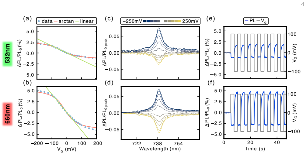
Aqueous electrolytic gating switches shallow silicon-vacancy centers in diamond between fluorescent SiV- and dark SiV0 states at biases below 200 mV.
A machine-rendered reading of the paper's core claim, the machinery that carries it, and where it could break.
Core claim
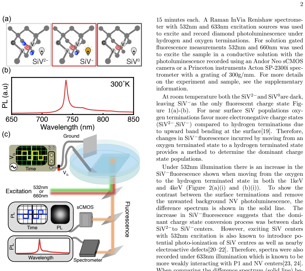
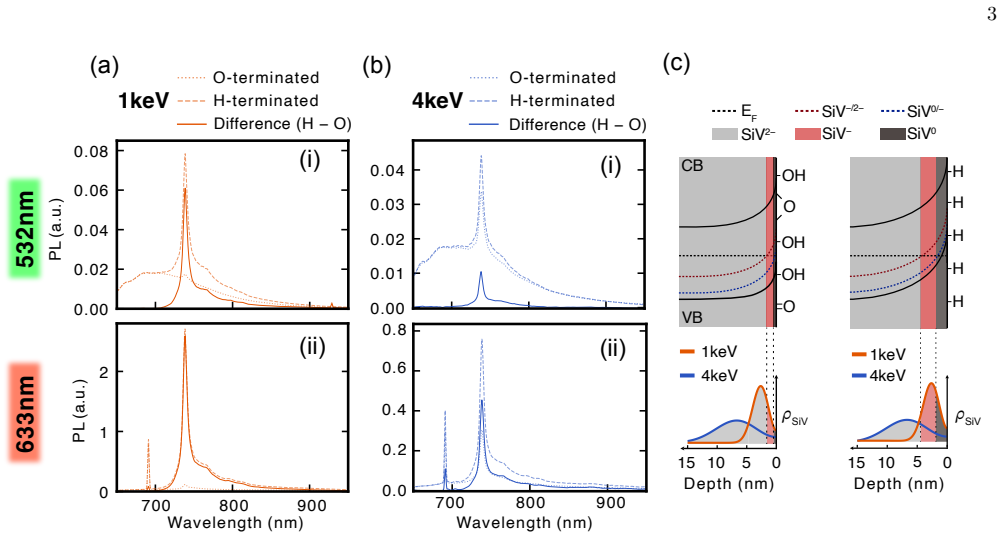
By combining low-energy ion implantation with tailored oxygen and hydrogen terminations, regimes that maximise the fluorescent SiV- population are mapped; reversible SiV- to SiV0 conversion is then realized using aqueous electrolytic gating with sub-200 mV biases and low optical powers.
What carries the argument
Aqueous electrolytic gating that applies a local electrochemical potential to modulate the charge state of shallow implanted SiV centers.
If this is right
- Low-power electrical addressing of SiV ensembles becomes feasible for integrated quantum photonics circuits.
- Near-infrared voltage sensing in biological systems is enabled without high optical excitation powers.
- Surface termination choices can be used to preset the dominant charge state before electrical gating is applied.
- Control extends to defects located less than 15 nm from the diamond surface.
Where Pith is reading between the lines
- The same gating approach may allow dynamic stabilization of other near-surface color centers whose charge states limit coherence or brightness.
- Integration with microfluidic channels could create compact sensors that combine electrical gating with optical readout in liquid environments.
- If the gate-induced potential landscape is mapped, the method could be adapted to create addressable arrays of individually controllable emitters.
Load-bearing premise
Observed fluorescence intensity changes arise from reversible conversion between the SiV- and SiV0 charge states rather than from unrelated surface chemistry or optical artifacts.
What would settle it
A measurement that directly determines the SiV charge state (for example by resonant excitation spectra or spin resonance) while the fluorescence intensity changes under gating, showing no population shift between SiV- and SiV0.
Figures
read the original abstract
Silicon-vacancy (SiV) centers in diamond combine near-infrared emission with solid-state robustness, but their performance hinges on isolating favorable defect charge states. We demonstrate static and dynamic control of ultra-shallow (<15 nm) SiV ensembles in type IIa diamond. By combining low-energy ion implantation with tailored oxygen and hydrogen terminations, we map regimes that maximise the fluorescent SiV- population over dark charge states. We then realize reversible SiV- to SiV0 conversion using aqueous electrolytic gating with sub-200 mV biases and low optical powers. Our results enable low-power electrical control of SiV ensembles for integrated quantum photonics and biologically compatible voltage imaging in the near-infrared.
Editorial analysis
A structured set of objections, weighed in public.
Referee Report
Summary. The manuscript reports experimental control of charge states in ultra-shallow (<15 nm) SiV ensembles in type-IIa diamond. Static control is achieved via low-energy implantation combined with oxygen and hydrogen surface terminations to maximize the fluorescent SiV- population. Dynamic reversible conversion between SiV- and SiV0 is then demonstrated using aqueous electrolytic gating at biases below 200 mV and low optical powers, with fluorescence intensity changes interpreted as the signature of charge-state switching.
Significance. If the mapping from fluorescence to charge state is secured, the result would enable low-voltage electrical control of SiV ensembles, with potential applications in integrated quantum photonics and near-infrared bio-compatible voltage imaging. The work is an experimental demonstration that combines established implantation and termination techniques with solution gating; no parameter-free derivations or machine-checked proofs are present.
major comments (1)
- [gating results] Results on electrolytic gating (section describing fluorescence vs. bias data): the central claim that sub-200 mV gating produces reversible SiV- ↔ SiV0 conversion rests on equating observed fluorescence intensity changes with charge-state population shifts. For <15 nm ensembles this mapping is load-bearing, yet the provided data appear to lack direct spectral confirmation (e.g., resolved ZPL peaks at the known SiV- and SiV0 wavelengths) or independent charge readout to rule out surface, electrolyte, or photo-charging artifacts.
minor comments (1)
- [abstract] Abstract and introduction: the phrasing 'maximise the fluorescent SiV- population over dark charge states' should be accompanied by a brief statement of how the population fractions were quantified (e.g., via calibrated spectra or lifetime measurements).
Simulated Author's Rebuttal
We thank the referee for their careful review and for identifying the key interpretive step in our electrolytic gating results. We address the concern point-by-point below and indicate the revisions we will make.
read point-by-point responses
-
Referee: Results on electrolytic gating (section describing fluorescence vs. bias data): the central claim that sub-200 mV gating produces reversible SiV- ↔ SiV0 conversion rests on equating observed fluorescence intensity changes with charge-state population shifts. For <15 nm ensembles this mapping is load-bearing, yet the provided data appear to lack direct spectral confirmation (e.g., resolved ZPL peaks at the known SiV- and SiV0 wavelengths) or independent charge readout to rule out surface, electrolyte, or photo-charging artifacts.
Authors: We agree that the fluorescence-to-charge-state mapping is central and that direct spectral confirmation would strengthen the claim. The manuscript interprets reversible intensity changes under sub-200 mV bias and low optical power as SiV- ↔ SiV0 conversion on the basis of (i) the known ZPL wavelengths and filter transmission, (ii) the correlation with the static termination-dependent populations established earlier in the work, and (iii) power-dependence controls intended to limit photo-charging. We acknowledge that these controls do not constitute independent charge readout or fully resolved ZPL spectra. We will therefore revise the gating section to include a more explicit discussion of possible artifacts together with any available spectral traces or additional control data that can be extracted from the existing measurements. revision: partial
Circularity Check
No circularity: experimental demonstration with no derivations or fitted parameters
full rationale
The paper reports experimental control of SiV charge states via surface termination and electrolytic gating, relying on observed fluorescence intensity changes. No equations, parameter fits, or derivation chains appear in the provided text. The central claim equates fluorescence shifts with charge-state conversion, but this is an interpretive mapping from data rather than a mathematical reduction to inputs by construction. No self-citations are load-bearing for any derivation, and the work contains no ansatzes, uniqueness theorems, or renamings of known results. This is a standard experimental report whose validity rests on external benchmarks (spectroscopy, controls) outside any internal circular loop.
Axiom & Free-Parameter Ledger
Reference graph
Works this paper leans on
-
[1]
Kurtsiefer, S
C. Kurtsiefer, S. Mayer, P. Zarda, and H. Weinfurter, Stable Solid-State Source of Single Photons, Physical Re- view Letters85, 290 (2000)
2000
-
[2]
A. Beveratos, Single Photon Quantum Cryptog- raphy, Physical Review Letters89, 10.1103/Phys- RevLett.89.187901 (2002)
-
[3]
Sipahigil, K
A. Sipahigil, K. D. Jahnke, L. J. Rogers, T. Ter- aji, J. Isoya, A. S. Zibrov, F. Jelezko, and M. D. Lukin, Indistinguishable Photons from Separated Silicon- Vacancy Centers in Diamond, Physical Review Letters 6 113, 113602 (2014)
2014
-
[4]
Waltrich, M
R. Waltrich, M. Klotz, V. N. Agafonov, and A. Kubanek, Two-photon interference from silicon-vacancy centers in remote nanodiamonds, Nanophotonics12, 3663 (2023)
2023
-
[5]
D. J. McCloskey, N. Dontschuk, A. Stacey, C. Pattinson, A. Nadarajah, L. T. Hall, L. C. L. Hollenberg, S. Prawer, and D. A. Simpson, A diamond voltage imaging micro- scope, Nature Photonics16, 730 (2022)
2022
-
[6]
Bar-Gill, L
N. Bar-Gill, L. M. Pham, A. Jarmola, D. Budker, and R. L. Walsworth, Solid-state electronic spin coherence time approaching one second, Nature Communications 4, 1743 (2013)
2013
-
[7]
Gruber, A
A. Gruber, A. Dr¨ abenstedt, C. Tietz, L. Fleury, J. Wrachtrup, and C. von Borczyskowski, Scanning Con- focal Optical Microscopy and Magnetic Resonance on Single Defect Centers, Science276, 2012 (1997)
2012
-
[8]
E. Neu, D. Steinmetz, J. Riedrich-M¨ oller, S. Gsell, M. Fischer, M. Schreck, and C. Becher, Single photon emission from silicon-vacancy colour centres in chemical vapour deposition nano-diamonds on iridium, New Jour- nal of Physics13, 025012 (2011)
2011
-
[9]
W. Liu, M. N. A. Alam, Y. Liu, V. N. Agafonov, H. Qi, K. Koynov, V. A. Davydov, R. Uzbekov, U. Kaiser, T. Lasser, F. Jelezko, A. Ermakova, and T. Weil, Silicon- Vacancy Nanodiamonds as High Performance Near- Infrared Emitters for Live-Cell Dual-Color Imaging and Thermometry, Nano Letters22, 2881 (2022)
2022
-
[10]
Golubewa, Y
L. Golubewa, Y. Padrez, S. Malykhin, T. Kulahava, E. Shamova, I. Timoshchenko, M. Franckevicius, A. Sel- skis, R. Karpicz, A. Obraztsov, Y. Svirko, and P. Kuzhir, All-Optical Thermometry with NV and SiV Color Cen- ters in Biocompatible Diamond Microneedles, Advanced Optical Materials10, 2200631 (2022)
2022
-
[11]
U. F. S. D’Haenens-Johansson, A. M. Edmonds, B. L. Green, M. E. Newton, G. Davies, P. M. Martineau, R. U. A. Khan, and D. J. Twitchen, Optical properties of the neutral silicon split-vacancy center in diamond, Physical Review B84, 245208 (2011)
2011
-
[12]
B. C. Rose, D. Huang, Z.-H. Zhang, P. Stevenson, A. M. Tyryshkin, S. Sangtawesin, S. Srinivasan, L. Loudin, M. L. Markham, A. M. Edmonds, D. J. Twitchen, S. A. Lyon, and N. P. de Leon, Observation of an environmen- tally insensitive solid-state spin defect in diamond, Sci- ence361, 60 (2018)
2018
-
[13]
Zhang, J
Z.-H. Zhang, J. A. Zuber, L. V. H. Rodgers, X. Gui, P. Stevenson, M. Li, M. Batzer, M. Grimau Puigib- ert, B. J. Shields, A. M. Edmonds, N. Palmer, M. L. Markham, R. J. Cava, P. Maletinsky, and N. P. De Leon, Neutral Silicon Vacancy Centers in Undoped Diamond via Surface Control, Physical Review Letters130, 166902 (2023)
2023
-
[14]
Silicon-Vacancy
D. G. Pasternak, A. A. Zhivopistsev, A. M. Romshin, O. S. Kudryavtsev, R. H. Bagramov, V. P. Filonenko, N. I. Kargin, and I. I. Vlasov, Effect of H-Terminated Surfaces on “Silicon-Vacancy” Fluorescence in High- Pressure Nanodiamonds, Nanomaterials15, 1842 (2025)
2025
-
[15]
D. K. Angell, S. Li, H. Utzat, M. L. S. Thurston, Y. Liu, J. Dahl, R. Carlson, Z.-X. Shen, N. Melosh, R. Sinclair, and J. A. Dionne, Unraveling sources of emission het- erogeneity in Silicon Vacancy color centers with cryo- cathodoluminescence microscopy, Proceedings of the Na- tional Academy of Sciences121, e2308247121 (2024)
2024
-
[16]
J. A. Zuber, M. Li, M. Grimau Puigibert, J. Happacher, P. Reiser, B. J. Shields, and P. Maletinsky, Shallow Silicon Vacancy Centers with Lifetime-Limited Optical Linewidths in Diamond Nanostructures, Nano Letters 23, 10901 (2023)
2023
-
[17]
Gali and J
A. Gali and J. R. Maze, Ab initio study of the split silicon-vacancy defect in diamond: Electronic structure and related properties, Physical Review B88, 235205 (2013)
2013
-
[18]
Garcia-Arellano, G
G. Garcia-Arellano, G. I. L´ opez-Morales, N. B. Manson, J. Flick, A. A. Wood, and C. A. Meriles, Photo-Induced Charge State Dynamics of the Neutral and Negatively Charged Silicon Vacancy Centers in Room-Temperature Diamond, Advanced Sciencen/a, 2308814 (2024)
2024
-
[19]
D. A. Broadway, N. Dontschuk, A. Tsai, S. E. Lillie, C. T.-K. Lew, J. C. McCallum, B. C. Johnson, M. W. Doherty, A. Stacey, L. C. L. Hollenberg, and J.-P. Teti- enne, Spatial mapping of band bending in semiconductor devices using in situ quantum sensors, Nature Electronics 1, 502 (2018)
2018
-
[20]
Nicolas, T
L. Nicolas, T. Delord, P. Huillery, C. Pellet-Mary, and G. H´ etet, Sub-GHz Linewidth Ensembles of SiV Centers in a Diamond Nanopyramid Revealed by Charge State Conversion, ACS Photonics6, 2413 (2019)
2019
-
[21]
Zhang, A
Z.-H. Zhang, A. M. Edmonds, N. Palmer, M. L. Markham, and N. P. de Leon, Neutral Silicon-Vacancy Centers in Diamond via Photoactivated Itinerant Carri- ers, Physical Review Applied19, 034022 (2023)
2023
-
[22]
Dhomkar, P
S. Dhomkar, P. R. Zangara, J. Henshaw, and C. A. Mer- iles, On-Demand Generation of Neutral and Negatively Charged Silicon-Vacancy Centers in Diamond, Physical Review Letters120, 117401 (2018)
2018
-
[23]
H¨ außler, G
S. H¨ außler, G. Thiering, A. Dietrich, N. Waasem, T. Ter- aji, J. Isoya, T. Iwasaki, M. Hatano, F. Jelezko, A. Gali, and A. Kubanek, Photoluminescence excitation spec- troscopy of SiV - and GeV - color center in diamond, New Journal of Physics19, 063036 (2017)
2017
-
[24]
A. A. Wood, A. Lozovoi, R. M. Goldblatt, C. A. Meriles, and A. M. Martin, Wavelength dependence of nitrogen vacancy center charge cycling, Physical Review B109, 134106 (2024)
2024
-
[25]
Thiering and A
G. Thiering and A. Gali,Ab InitioMagneto-Optical Spectrum of Group-IV Vacancy Color Centers in Dia- mond, Physical Review X8, 021063 (2018)
2018
-
[26]
Kronik and Y
L. Kronik and Y. Shapira, Surface photovoltage spec- troscopy of semiconductor structures: At the crossroads of physics, chemistry and electrical engineering, Surface and Interface Analysis31, 954 (2001)
2001
-
[27]
Rezek, C
B. Rezek, C. E. Nebel, and M. Stutzmann, Hydrogenated diamond surfaces studied by atomic and Kelvin force mi- croscopy, Diamond and Related Materials 14th European Conference on Diamond, Diamond-Like Materials, Car- bon Nanotubes, Nitrides and Silicon Carbide,13, 740 (2004)
2004
-
[28]
A. Wood, A. Lozovoi, Z.-H. Zhang, S. Sharma, G. I. L´ opez-Morales, H. Jayakumar, N. P. de Leon, and C. A. Meriles, Room-Temperature Photochromism of Silicon Vacancy Centers in CVD Diamond, Nano Letters23, 1017 (2023)
2023
-
[29]
K. Bray, D. Y. Fedyanin, I. A. Khramtsov, M. O. Bilokur, B. Regan, M. Toth, and I. Aharonovich, Electrical ex- citation and charge-state conversion of silicon vacancy color centers in single-crystal diamond membranes, Ap- plied Physics Letters116, 101103 (2020)
2020
- [30]
-
[31]
Rieger, V
M. Rieger, V. Villafa˜ ne, L. M. Todenhagen, S. Matthies, S. Appel, M. S. Brandt, K. M¨ uller, and J. J. Finley, Fast optoelectronic charge state conversion of silicon vacancies in diamond, Science Advances10, eadl4265 (2024)
2024
-
[32]
Ristein, M
J. Ristein, M. Riedel, M. Stammler, B. F. Mantel, and L. Ley, Surface conductivity of nitrogen-doped diamond, Diamond and Related Materials 12th European Con- ference on Diamond, Diamond- Like Materials, Carbon Nanotubes, Nitrides & Silicon Carbide,11, 359 (2002)
2002
-
[33]
M. Zou, J. Bohon, J. Smedley, J. Distel, K. Schmitt, R.- Y. Zhu, L. Zhang, and E. M. Muller, Proton radiation effects on carrier transport in diamond radiation detec- tors, AIP Advances10, 025004 (2020)
2020
-
[34]
J.-P. Tetienne, Spin properties of dense near-surface en- sembles of nitrogen-vacancy centers in diamond, Physical Review B97, 10.1103/PhysRevB.97.085402 (2018)
-
[35]
A. J. Healey, A. M. Jakob, D. J. McCloskey, P. Reineck, D. T. Vallury, B. C. Gibson, D. A. Simpson, A. Stacey, and N. Dontschuk, Production of High Yield, Ultra- Shallow Nitrogen-Vacancy Centre Ensembles Through High Purity Forming gas Annealing, Advanced Func- tional Materialsn/a, e25576 (2026)
2026
-
[36]
Jingu, K
Y. Jingu, K. Hirama, and H. Kawarada, Ultrashal- low TiC Source/Drain Contacts in Diamond MOSFETs Formed by Hydrogenation-Last Approach, IEEE Trans- actions on Electron Devices57, 966 (2010)
2010
-
[37]
Depover and K
T. Depover and K. Verbeken, The effect of TiC on the hydrogen induced ductility loss and trapping behavior of Fe-C-Ti alloys, Corrosion Science112, 308 (2016)
2016
-
[38]
T. Boot, A. Suresh Kumar, S. Eswara, P. K¨ ommelt, A. B¨ ottger, and V. Popovich, Hydrogen trapping and embrittlement of titanium- and vanadium carbide- containing steels after high-temperature hydrogen charg- ing, Journal of Materials Science59, 7873 (2024)
2024
-
[39]
Grotz, M
B. Grotz, M. V. Hauf, M. Dankerl, B. Naydenov, S. Pez- zagna, J. Meijer, F. Jelezko, J. Wrachtrup, M. Stutz- mann, F. Reinhard, and J. A. Garrido, Charge state ma- nipulation of qubits in diamond, Nature Communications 3, 729 (2012)
2012
-
[40]
J. Icha, M. Weber, J. C. Waters, and C. Norden, Photo- toxicity in live fluorescence microscopy, and how to avoid it, BioEssays39, 1700003 (2017)
2017
-
[41]
Croce and G
A. Croce and G. Bottiroli, Autofluorescence Spec- troscopy and Imaging: A Tool for Biomedical Research and Diagnosis, European Journal of Histochemistry : EJH58, 2461 (2014)
2014
discussion (0)
Sign in with ORCID, Apple, or X to comment. Anyone can read and Pith papers without signing in.