REVIEW 4 major objections 7 minor 24 references
Improving feature resolution and pore back effect in focused ion beam tomography of porous GaN thin films
T0 review · 4 major / 7 minor · reviewed 2026-07-09 · glm-5.2
Pith's one-line read Rotating FIB tomography 90° cuts pore back effect in porous GaN
desk verdict Useful rotated-geometry method for FIB-SEM tomography of porous GaN; metrics are qualitative, generalization claim overstated read the letter →
The pith
A machine-rendered reading of the paper's core claim, the machinery that carries it, and where it could break.
The reading
What carries the argument
The pore back effect is the central phenomenon: when imaging through transparent voids in SEM-based tomography, secondary and back-scattered electrons from the solid material forming the back wall of a pore are detected and contribute unwanted contrast to frames captured at shallower milling depths than the feature's true position, producing a directional smearing of features along the milling axis in the reconstructed tomograph.
What would settle it
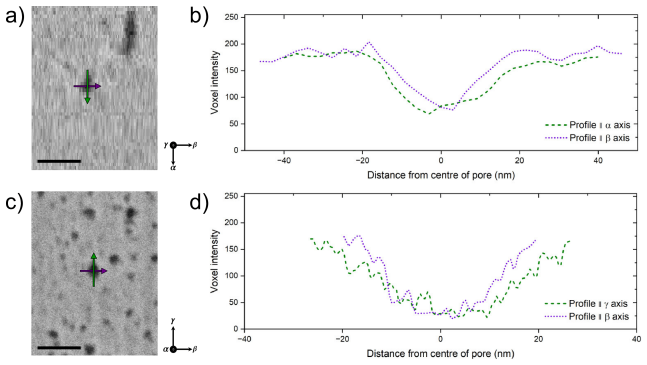
If the intensity-distribution histograms and feature-anisotropy line profiles showed no systematic difference between the two tomography orientations across all three samples, the claim that plan-view geometry mitigates the pore back effect would be unsupported.
Extended reading notes
Core claim
The plan-view tomography orientation — milling direction perpendicular to the film surface and thus parallel to the long axis of vertically-etched pores — significantly reduces the pore back effect compared to conventional cross-sectional tomography, and two voxel-intensity-based metrics (intensity distribution histograms and feature anisotropy line profiles) provide the first quantitative framework for assessing the severity of this imaging artifact in porous thin films.
Load-bearing premise
The method's advantage depends on pores being predominantly vertically aligned — etching downward from the film surface. For highly branched or isotropic pore structures, the advantage shrinks because no orientation can align the milling direction with a dominant pore axis, and the paper's own most challenging sample (Sample 3) shows the weakest improvement.
Signed reviews
Editorial analysis
A structured set of objections, weighed in public.
Referee Report
Summary. This manuscript presents a new 'plan-view' FIB-SEM tomography methodology for porous GaN thin films, in which the experiment is rotated 90 degrees so that the milling direction is perpendicular to the film surface and aligned with the long axis of vertically propagating pores. The approach is compared against conventional 'cross-sectional' tomography on three samples with different pore morphologies. Two voxel-intensity-based metrics are introduced to assess the pore back effect: intensity distribution histograms and feature anisotropy line profiles. The authors find that plan-view tomography mitigates the pore back effect for vertically aligned pores (Samples 1 and 2) and offers marginal improvement for branched pores (Sample 3). The paper is well-motivated, the experimental comparison is internally consistent, and the methodology is described in sufficient detail for replication.
Significance. The pore back effect is a well-known but poorly quantified artefact in FIB-SEM tomography of porous materials, and this work represents a serious attempt to address it through both experimental geometry and quantitative assessment tools. The plan-view setup is a practical contribution that other groups working on mesoporous thin films can adopt. The intensity histogram comparison (e.g., Fig. 14) provides a visually compelling and physically motivated demonstration of the difference between the two approaches. The line-profile anisotropy metric (Fig. 15) is a useful diagnostic. The work is relevant to the porous GaN community and, more broadly, to FIB-SEM characterisation of mesoporous thin films on substrates.
major comments (4)
- §3 and §4: The intensity-based 'formalisms' are presented as quantitative tools, but no scalar metric or statistical test is defined. The histograms in Figs. 14, 19, and 24 are compared visually ('the more the distribution resembles the simple two-peak ideal case, the less the effect of the pore back has been'). The line-profile anisotropy (Fig. 15) is demonstrated on a single pore per sample without aggregation. To support the claim that the pore back effect can be 'quantified,' the authors should define at least one scalar quantity (e.g., a bimodality index for the histogram, or an asymmetry ratio for the line profiles) and report it for both orientations across all three samples. Without this, the assessment remains qualitative despite the language of 'formalisms' and 'quantification.'
- §4.3 and Abstract: The abstract claims the approach 'significantly mitigates the pore back effect in porous GaN thin films with a range of pore morphologies.' However, for Sample 3 (branched pores), the authors concede the advantage is 'contentious' and 'marginal' (§4.3), the plan-view dataset suffered overexposure (Fig. 24), and the reconstructed cross-section shows 'very poor contrast' in the top half. The abstract should be revised to accurately scope the claim — e.g., 'for porous GaN thin films with vertically aligned pore morphologies, with more limited improvement for branched morphologies' — or the Sample 3 data should be re-acquired without overexposure to support the broader claim.
- §3: No ground-truth validation is provided to confirm that the intensity distribution differences between the two orientations are attributable specifically to the pore back effect rather than to other systematic differences between the setups (mounting geometry, charging, curtaining, tracking structure dimensions, surface quality). The authors acknowledge several such confounders (curtaining in Fig. 13b, mounting tilt, software glitching in Figs. 18c and 23c). While the physical argument is sound, at least one of the following would strengthen the causal claim: (a) Monte Carlo electron scattering simulation of the expected pore back signal for each geometry, (b) a phantom sample with known pore geometry, or (c) a more explicit discussion of why the confounders cannot account for the observed intensity differences. The authors gesture toward simulation in §5 ('It may therefore be of знач
- §4.1, Fig. 15: The line-profile anisotropy metric is noted to be inapplicable to the plan-view tomograph of Sample 1 because 'there is no front wall of the pore with GaN' and the back wall is up to 1 µm away. The authors state the metric is introduced 'only to be applied to suitable morphologies.' This limits the generality of the metric and should be stated more prominently, ideally in §3 where the metric is defined, rather than only at the end of §4.1.
minor comments (7)
- §2.2.2: The sentence beginning 'The total range of the m-axis of the stage in the Crossbeam 540 instrument presented another limitation...' is grammatically awkward and could be clarified.
- Figures 12-13, 17-18, 22-23: The axis labels on the bottom-right of the images are referenced but not always legible in the figure descriptions. Ensure axis labels are clearly readable in the final figures.
- §4.2, Fig. 19 caption: The caption states 'the value of intensity plotted against the fraction of total voxels' but the y-axis label is not explicitly described. Clarify whether the histograms are normalised.
- §4.3: 'the contrast is also sharper than it is in the input frames for this tomograph, such as in Figure 17a' — this reference to Fig. 17a (Sample 2) appears to be an error; it should likely reference a figure from Sample 3 (Fig. 22a).
- §5: The suggestion of a simulation workflow is valuable but somewhat underdeveloped. Consider moving this to an outlook section or expanding briefly on what inputs would be needed.
- Reference [13] is cited as 'J. Appl. Phys. 139 (17) (2026) 175702' — verify this is not a preprint or in-press reference and that the year/volume are correct.
- The term 'pore back effect' is introduced in §1 but the alternative 'shine-through artefacts' (ref [15]) is mentioned only once. Consider using both terms initially for searchability.
Circularity Check
No circularity found; the paper is an experimental A/B comparison with physically-motivated metrics
full rationale
The paper's derivation chain is self-contained and non-circular. The central claim has two components: (1) plan-view tomography mitigates the pore back effect, and (2) voxel intensity-based formalisms quantify it. For (1), the argument proceeds from physical first principles — the pore back effect arises because electrons scatter from the back wall of pores (§3, citing ref [15] externally), so aligning the milling direction with the pore's longest dimension maximizes the distance to the back wall. This is tested by a direct A/B experimental comparison on the same three samples under identical beam conditions (2 kV, 65 pA), with no fitted parameters. For (2), the two metrics are defined from the physics of electron-void interaction, not from the result they measure: the intensity histogram formalism (§3, Fig 10) argues that a binary GaN/void composite should show two intensity peaks, and the pore back effect smears the void peak toward higher intensities — this is a physical prediction, not a definition that assumes the conclusion. The feature anisotropy metric (§3, Fig 9) argues that the pore back effect introduces asymmetry along the milling direction but not perpendicular to it — again physically derived, then tested on extracted line profiles (Figs 15, 20, 25). No parameter is fitted to a subset of data and then 'predicted' on related data. Self-citations (refs [13], [20], [24]) are used for contextual background on porous GaN structure and prior tomography work; none are load-bearing for the method or metrics presented here. The paper's weaknesses (lack of ground-truth validation, overgeneralization to 'a range of pore morphologies' when Sample 3 shows marginal advantage, qualitative rather than scalar metrics) are correctness and generalizability concerns, not circularity.
Assumptions & free parameters
free parameters (4)
- Electron beam accelerating voltage =
2 kV
- Electron probe current =
65 pA
- Image pixel size =
1 nm
- Average slice thickness =
~5.7-5.9 nm
assumptions (3)
- domain assumption Porous GaN is effectively a binary composite of GaN matrix and void, where void is completely transparent to electrons.
- domain assumption Electrochemically etched GaN with surface-terminating doped layers produces pores that etch predominantly downward from the surface.
- domain assumption The pore back effect is the dominant source of feature anisotropy along the milling direction in FIB-SEM tomography of porous materials.
Cite this review
Pith. "Pith review of Improving feature resolution and pore back effect in focused ion beam tomography of porous GaN thin films." pith.science (2026). https://pith.science/paper/VD3HFR2Z
@misc{pith2026260707273,
  author       = {Pith},
  title        = {Pith review of: Improving feature resolution and pore back effect in focused ion beam tomography of porous GaN thin films},
  year         = {2026},
  howpublished = {\url{https://pith.science/paper/VD3HFR2Z}},
  note         = {Machine review of arXiv:2607.07273}
}
read the original abstract
Porous gallium nitride (GaN) is a mesoporous crystalline material, typically in the form of a thin film on an unlike substrate, prepared by electrochemically etching conductive GaN. The use of porous GaN in electronics and optoelectronics is rapidly expanding, but is held back significantly by a lack of structural control and understanding of the principles of pore formation from underlying electrochemical mechanisms, where high-quality characterisation of pore morphology is essential to understanding these principles. Focused ion beam (FIB) tomography is an invaluable tool for such characterisation, but is hindered greatly by the pore back effect, where unwanted contrast appears in an image due to electrons scattering out from the back wall of a pore. No major attempts to formally quantify or assess the extent of the effect for different tomography experiments has been demonstrated. In this work, we demonstrate an advanced methodology for performing FIB tomography on porous GaN thin films, where the experiment is rotated to image pores perpendicular to the surface of the sample, and introduce new voxel intensity-based formalisms for assessing the impact of the pore back effect based on voxel intensities for individual features and the whole dataset. The new approach, which requires more complex preliminary setup, is found to significantly mitigate the pore back effect in porous GaN thin films with a range of pore morphologies without increasing the total experimental duration. The pore back effect can thus be quantified and mitigated in FIB tomography of porous GaN and similar mesoporous thin films.
Figures


Figures from the paper (22 more)




Reference graph
Works this paper leans on
-
[1]
Y. Zhang, S.-W. Ryu, C. Yerino, B. Leung, Q. Sun, Q. Song, H. Cao, J. Han, A conductivity-based selective etching for next generation 45 GaN devices, physica status solidi (b) 247 (7) (2010) 1713–1716. doi:doi.org/10.1002/pssb.200983650
-
[2]
Y. Calahorra, B. Spiridon, A. Wineman, T. Busolo, P. Griffin, P. K. Szewczyk, T. Zhu, Q. Jing, R. Oliver, S. Kar-Narayan, Enhanced piezoelectricity and electromechanical efficiency in semiconducting GaN due to nanoscale porosity, Applied Materials Today 21 (2020) 100858. doi:doi.org/10.1016/j.apmt.2020.10085
- [3]
-
[5]
T. R. Harris-Lee, B. Thornley, J. Zhang, M. J. Kappers, R. A. Oliver, Porous GaN: Anion-Specific Electrochemical Etch- ing Mechanisms and Morphological Control, ACS Applied Mate- rials & Interfaces 17 (47) (2025) 64931–64941, pMID: 41230933. doi:doi.org/10.1021/acsami.5c18520
-
[6]
W.-T. Huang, L.-X. Hong, R.-S. Liu, Nanostructure Control of GaN by Electrochemical Etching for Enhanced Perovskite Quantum Dot LED Backlighting, ACS Applied Materials & Interfaces 15 (33) (2023) 39505– 39512, pMID: 37551922. doi:doi.org/10.1021/acsami.3c06257
-
[7]
S. H. Abud, Z. Hassan, F. Yam, Enhancement of Structural and Op- tical Properties of Porous In0.27Ga0.73N Thin Film Synthesized Using Electrochemical Etching Technique, International Journal of Electro- chemical Science 7 (10) (2012) 10038–10046. doi:doi.org/10.1016/S1452- 3981(23)16256-0
-
[8]
D. Chen, H. Xiao, J. Han, Nanopores in GaN by electrochemical an- odization in hydrofluoric acid: Formation and mechanism, Journal of Applied Physics 112 (6) (2012) 064303. doi:doi.org/10.1063/1.4752259
-
[9]
A. Ramizy, Z. Hassan, K. Omar, Porous GaN on Si(111) and its applica- tion to hydrogen gas sensor, Sensors and Actuators B: Chemical 155 (2) (2011) 699–708. doi:doi.org/10.1016/j.snb.2011.01.034. 46
Show all 24 references
-
[10]
Benton, J
J. Benton, J. Bai, T. Wang, Utilisation of GaN and InGaN/GaN with nanoporous structures for water splitting, Applied Physics Letters 105 (22) (2014) 223902. doi:doi.org/10.1063/1.4903246
2014 doi
-
[11]
X. Bai, S. M. Fairclough, L. Dai, M. Sarkar, P. H. Griffin, A. Gundimeda, Y. Sun, N. C. Greenham, M. I. Dar, R. A. Oliver, R. H. Friend, Enhanced Excitonic Nature of MAPbBr3 Nanocrystals in Nanoporous GaN, Advanced Optical Materials 12 (20) (2024) 2400221. doi:doi.org/10.1002/...
2024 doi
-
[12]
Keller, S
S. Keller, S. S. Pasayat, C. Gupta, S. P. DenBaars, S. Nakamura, U. K. Mishra, Patterned III-Nitrides on Porous GaN: Extending Elastic Relaxation from the Nano- to the Micrometer Scale, physica status solidi (RRL) – Rapid Research Letters 15 (11) (2021) 2100234. arXiv:https://...
2021 doi
-
[13]
Zhang, S
C. Zhang, S. H. Park, D. Chen, D.-W. Lin, W. Xiong, H.-C. Kuo, C.-F. Lin, H. Cao, J. Han, Mesoporous GaN for Photonic Engineer- ing—Highly Reflective GaN Mirrors as an Example, ACS Photonics 2 (7) (2015) 980–986. arXiv:https://doi.org/10.1021/acsphotonics.5b00216, doi:doi.org/...
2015 doi
-
[14]
Zhang, B
J. Zhang, B. Thornley, T. R. Harris-Lee, S. A. Dar, M. J. Kappers, R. A. Oliver, The impact of dislocation-mediated etching on the struc- ture of porous GaN, Journal of Applied Physics 139 (17) (2026) 175702. doi:doi.org/10.1063/5.0325215
2026 doi
-
[15]
T. Zhu, Y. Liu, T. Ding, W. Y. Fu, J. Jarman, C. X. Ren, R. V. Ku- mar, R. A. Oliver, Wafer-scale Fabrication of Non-Polar Mesoporous GaN Distributed Bragg Reflectors via Electrochemical Porosification, Scientific Reports 7 (1) (2017) 45344. doi:doi.org/10.1038/srep45344
2017 doi
-
[16]
I. A. Reimers, I. V. Safonov, I. V. Yakimchuk, Segmentation of 3D FIB- SEM data with pore-back effect, Journal of Physics: Conference Series 1368 (3) (2019) 032015. doi:doi.org/10.1088/1742-6596/1368/3/032015
2019 doi
-
[17]
Salzer, S
M. Salzer, S. Thiele, R. Zengerle, V. Schmidt, On the im- portance of FIB-SEM specific segmentation algorithms for 47 porous media, Materials Characterization 95 (2014) 36–43. doi:doi.org/10.1016/j.matchar.2014.05.014
2014 doi
-
[18]
Jørgensen, K
P. Jørgensen, K. Hansen, R. Larsen, J. Bowen, A framework for automatic segmentation in three dimensions of microstruc- tural tomography data, Ultramicroscopy 110 (3) (2010) 216–228. doi:doi.org/10.1016/j.ultramic.2009.11.013
2010 doi
-
[19]
Sciazko, Y
A. Sciazko, Y. Komatsu, A. Nakamura, Z. Ouyang, T. Hara, N. Shika- zono, 3D microstructures of solid oxide fuel cell Ni-YSZ anodes with carbon deposition, Chemical Engineering Journal 460 (2023) 141680. doi:doi.org/10.1016/j.cej.2023.141680
2023 doi
-
[20]
Neˇ cas, P
D. Neˇ cas, P. Klapetek, Gwyddion: an open-source software for SPM data analysis, Central European Journal of Physics 10 (2012) 181–188. doi:doi.org/10.2478/s11534-011-0096-2
2012 doi
-
[21]
Thornley, M
B. Thornley, M. Sarkar, S. Ghosh, M. Frentrup, M. J. Kappers, T. R. Harris-Lee, R. A. Oliver, A cascade model for the defect-driven etching of porous GaN distributed Bragg reflectors, Acta Materialia 308 (2026) 121957. doi:doi.org/10.1016/j.actamat.2026.121957
2026 doi
-
[22]
Medjahed, C
I. Medjahed, C. Licitra, S. Sadki, C. Pernel, Electrochemical Prediction Tool of Porous GaN Morphology, The Journal of Physical Chemistry C 128 (15) (2024) 6249–6258. doi:doi.org/10.1021/acs.jpcc.3c05297
2024 doi
-
[23]
Chen, J.-S
W. Chen, J.-S. Wu, X.-H. Xia, Porous Anodic Alumina with Contin- uously Manipulated Pore/Cell Size, ACS Nano 2 (5) (2008) 959–965, pMID: 19206493. doi:doi.org/10.1021/nn700389j
2008 doi
-
[24]
Kuntyi, G
O. Kuntyi, G. Zozulya, M. Shepida, Porous Silicon Formation by Elec- trochemical Etching, Advances in Materials Science and Engineering 2022 (1) (2022) 1482877. doi:doi.org/10.1155/2022/1482877
2022 doi
-
[25]
T. R. Harris-Lee, Y. Zhang, B. Thornley, J. Zhang, M. J. Kappers, R. A. Oliver, Analysis of in situ electrochemical characterization methods for porous GaN distributed Bragg reflectors, Journal of Applied Physics 139 (13) (2026) 135702. doi:doi.org/10.1063/5.0325374. 48
2026 doi
Reviewed July 9, 2026 · model on record in the stance chip above.
Discussion (0). Continue with ORCID to comment.