REVIEW 3 major objections 4 minor 8 references
Atomic Scale Ordering of Sulfur Vacancies Enhances Charge Transport in Monolayer MoS$_2$
T0 review · 3 major / 4 minor · reviewed 2026-08-06 · deepseek-v4-flash
Pith's one-line read Ordered sulfur vacancies transform a defective MoS2 monolayer into a band conductor
desk verdict A careful configurational study that makes a plausible case for vacancy-order-controlled transport, but the five-order current claim rests on unvalidated DFTB hybridization. read the letter →
The pith
A machine-rendered reading of the paper's core claim, the machinery that carries it, and where it could break.
The reading
What carries the argument
The load-bearing object is the vacancy miniband, a narrow band of delocalized electronic states created when the periodic 3x3 sulfur-vacancy lattice brings individual vacancy wavefunctions, which extend about 8 Å, into overlap. At the chosen 0.95 nm spacing the overlap is sufficient to produce a roughly 130 meV dispersive band; at the sparser 4x4 pattern the band narrows to about 15 meV, which the paper considers too small to support band-like transport. The miniband is computed with self-consistent density-functional tight-binding using a two-center orbital parameterization, spot-checked against a small set of spin-polarized density-functional single-point energies, and transport through 2,558-atom Au/MoS2/Au junctions is computed quantum mechanically within the same framework. The miniband does the work: it gives a near-unity transmission channel in the gap and a Fermi-level-aligned path for electron injection from the gold contacts.
What would settle it
A device experiment that patterns a 3x3 sulfur-vacancy lattice in monolayer MoS2 and compares it with random-vacancy and pristine channels would settle the claim: the ordered channel should show a dispersive $\sim$130 meV defect band in tunneling spectroscopy and, at 100 meV bias, a current orders of magnitude above random channels and close to the $\sim$1 µA the paper estimates. The absence of the dispersive band, or currents that do not separate by orders of magnitude, would falsify the mechanism.
Extended reading notes
Core claim
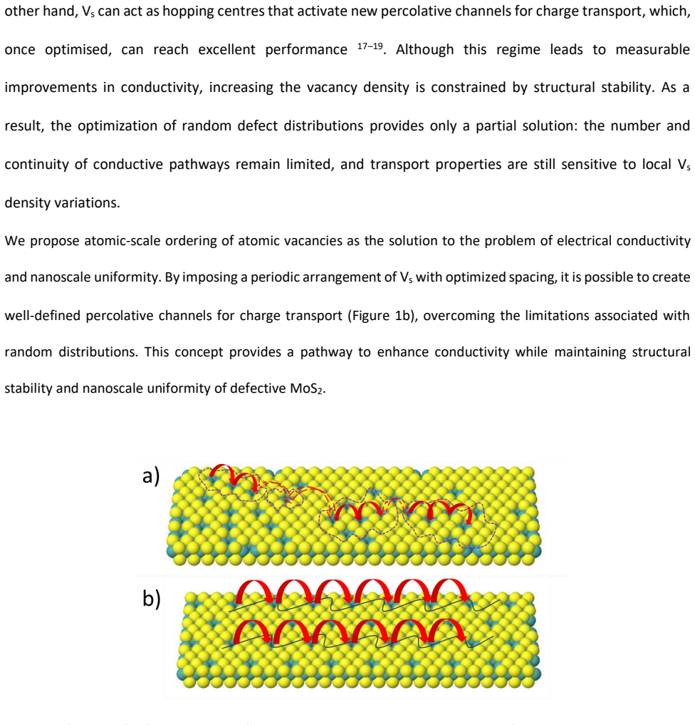
The paper's central discovery is that at a fixed vacancy concentration, the spatial phase of the defect lattice controls the transport regime. Four sulfur vacancies arranged as a periodic 3x3 pattern on the exposed sulfur sublattice (11.1% vacancy concentration, 0.95 nm nearest spacing) hybridize their midgap states into a dispersive in-gap miniband roughly 130 meV wide, while non-adjacent random arrangements of the same four vacancies yield only localized in-gap states. The ordered pattern is not the lowest-energy arrangement: of the 94 symmetry-inequivalent four-vacancy configurations, 14 sit more than 0.05 eV below it, but it belongs to a broad low-energy manifold, with 78.5% of all configurations within $\pm0.05$ eV, so it is an energetically reasonable periodic model. In Au/MoS2/Au device simulations, the gold Fermi level aligns with the vacancy-derived states, and the ordered array transmits current up to five orders of magnitude better than statistically equivalent random arrays, in the best cases matching or locally exceeding pristine MoS2.
Load-bearing premise
The result rests on the assumption that the approximate quantum model used for the simulations faithfully reproduces how vacancy states hybridize into a band and how much current flows, because only a handful of energies were checked against a more expensive method.
Editorial extensions
If this is right
- At fixed vacancy concentration, defect arrangement becomes a design parameter: periodic order can switch a channel from hopping-limited to band-like.
- An 11.1% vacancy density need not ruin conduction; the ordered pattern approaches pristine MoS2 current in the simulated junctions.
- Miniband width is a quantitative design target; the 3x3 pattern's roughly 130 meV width supports band transport, while a 4x4 pattern's roughly 15 meV width is too small.
- Random defect arrangements give device currents spread over orders of magnitude, so average density alone does not predict performance; percolating paths matter.
- Contact Fermi-level alignment with the defect band improves injection, so workfunction tuning of contacts could further enhance ordered-defect devices.
Reading between the lines
- A direct test follows from transport temperature dependence: ordered channels should show weakly temperature-dependent, band-like conductance, while random-vacancy channels should show thermally activated hopping; this could be measured in patterned devices without imaging the defects.
- The underlying principle likely transfers to other point defects in 2D semiconductors: heteroatoms, antisites, or vacancy complexes with midgap states could be periodically arranged to form in-gap bands in materials beyond MoS2.
- The simulations place ordered patterns under the contact pads in both ordered and random channels, so an implicit prediction is that contact-region ordering contributes to the enhancement; a device with ordered channels but random contacts would isolate where the benefit comes from.
Editorial analysis
A structured set of objections, weighed in public.
Referee Report
Summary. The manuscript investigates whether the spatial arrangement of sulfur vacancies in monolayer MoS2, at fixed concentration (11.1% in a 6x6 supercell), can change the electronic transport regime. Using density functional tight-binding (DFTB) for electronic structure and configurational energetics, and non-equilibrium Green's function (NEGF) transport simulations of Au/MoS2/Au junctions, the authors report that a periodic 3x3 vacancy array forms a 130 meV in-gap miniband, whereas random vacancy arrangements yield only localized states. They benchmark DFTB relative energies against PBE for eight configurations, analyze all 94 symmetry-inequivalent non-adjacent four-vacancy configurations, and find that the ordered pattern lies within a broad low-energy manifold. In device simulations, the ordered channel exhibits currents three to five orders of magnitude higher than random channels and can approach pristine MoS2. The paper concludes that atomic-scale defect ordering is a design principle for preserving conductivity in highly defective 2D semiconductors.
Significance. If the central result holds, the paper establishes a qualitatively new design axis—defect spatial order rather than defect concentration alone—for 2D materials, with clear falsifiable predictions (miniband dispersion, transmission peak, and I-V contrast). The configurational energetics analysis is a model of thoroughness: complete symmetry reduction of 16,659 valid arrangements into 94 inequivalent configurations, an orbit-size validation, and PBE cross-validation with Pearson r=0.986 make the energetic claim solid. The transport claim, however, is only as strong as the DFTB parametrization of vacancy-state hybridization and the contact model, which are not yet validated to the same standard.
major comments (3)
- [Methods, 'Targeted DFT validation of configurational energetics'; Results, Fig. 2] The central causal chain—ordered 3×3 vacancies → 130 meV in-gap miniband → up to five-order current enhancement—rests on the DFTB description of the hybridization of vacancy-derived states. The validation presented (PBE single-point relative energies, Pearson r=0.986; fixed-cell relaxations with RMS displacements of 0.025–0.026 Å) checks configurational energetics only, not the dispersion or width of the defect band. The text mentions a SI comparison of the DFTB bandstructure against Quantum Espresso, but no quantitative result is reported in the main text. Please provide a direct comparison of the DFTB and DFT (or hybrid-functional) bandstructures of the ordered 3×3 pattern, including the miniband width and the character of the in-gap states, and ideally an ab initio transmission calculation for a smaller device to confirm that the transmission peak near [-4.4, -4.1] eV is not an artifact of the Slater-Koster parameterization.
- [Transport across Au–MoS2–Au resistor, Fig. 4] In the device model, an ordered 3×3 defect pattern is assumed beneath the Au pads for both ordered and random channels, and the random pattern is periodically repeated in the semi-infinite leads. The authors explicitly acknowledge that this introduces possible artefacts, but the magnitude of the bias is not assessed. Because the ordered channel is perfectly matched to the ordered leads while the random channel is not, the transmission difference may reflect the lead/channel interface rather than the channel's intrinsic transport regime. Please include at least one control calculation with pristine or random-pattern leads for both channel types, or otherwise quantify the contact contribution to the transmission and I-V characteristics.
- [Transport across Au–MoS2–Au resistor, Fig. 6] The absolute currents and the current contrast depend on the imposed Au workfunction shift (set to give an effective WF of 4.5 eV, described as a 0.6 eV common shift relative to experimental values). The text asserts that the Fermi-level alignment is 'rather robust to small variations', but no data are shown. A sensitivity analysis of the I-V curves or transmission spectra as a function of the workfunction shift is necessary, because a shift of only a few tenths of an eV could move the Fermi level out of the 130 meV miniband and change the enhancement by orders of magnitude.
minor comments (4)
- [Abstract and Conclusions] The abstract states 'up to five orders of magnitude' and the conclusions say 'three to five orders'; the main text specifies that the best random configuration is three orders lower, while the worst is five orders lower. Since the maximum contrast is dominated by the worst sample among only 20 random realizations, please also report the median and the spread of the random currents so that the typical enhancement is clear.
- [References] Several references are duplicated with different numbers (e.g., Wang et al., Nat. Nanotechnol. 2012 appears as refs. 2 and 11; Hossen et al., Nanomaterials 2024 appears as refs. 3 and 10). Please consolidate the reference list.
- [Results and Discussion, second paragraph] The sentence beginning 'The localized wavefunctions that extend out to about 8 Å ...' is incomplete and grammatically unclear. Please rephrase to state the wavefunction extent and its consequence for vacancy-vacancy hybridization explicitly.
- [Fig. 2 caption] For panels (b) and (d), the caption says the background bands correspond to 'the same cell with 1 defect'. Please clarify whether this refers to a 6x6 supercell with a single vacancy and how the band folding is performed, so the comparison is unambiguous.
Circularity Check
No significant circularity: the miniband and current contrast are computed from externally parameterized DFTB and independent random references, not fitted to the conclusion.
full rationale
The paper's central claim—that ordered 3x3 sulfur-vacancy arrays create a ~130 meV in-gap miniband and produce up to five-orders-of-magnitude higher NEGF currents than random arrays—is a computed result, not a fitted one. The Slater-Koster parameters are taken from Heine's periodic table (external reference 35), and the configurational energetics are validated against PBE single points (Pearson r = 0.986, MAE = 0.027 eV). Random reference configurations are generated independently at the same vacancy concentration with the same non-adjacent constraint. The Au workfunction shift to 4.5 eV is justified by experimental ionization potentials and electron affinities plus a common -0.6 eV shift, not by the target current value; it sets the injection alignment and is reported as robust to small variations. Self-citations (refs. 13, 14, 20, 37, 38) concern method implementation, DFTB/NEGF formalism, and experimental nanopatterning feasibility, none of which is load-bearing for the electronic-structure or transport derivation. The ordered pattern was selected partly because 0.95 nm vacancy spacing is experimentally relevant, but the paper separately establishes that this pattern is not energetically anomalous within the complete 94-configuration ensemble, so the transport enhancement is not forced by construction. No equation or parameter is defined in terms of the predicted outcome; the comparison against random distributions provides an independent baseline. Overall, the derivation is self-contained apart from minor, non-load-bearing self-citations.
Assumptions & free parameters
free parameters (3)
- Effective Au workfunction shift =
4.5 eV effective (corresponds to 5.10 eV real Au WF)
- Ordered 3x3 vacancy pattern spacing =
0.95 nm, 11.1% vacancies
- Adjacent-vacancy exclusion distance =
3.5 Å
assumptions (6)
- domain assumption DFTB with Heine's periodic table MoS2 Slater-Koster parameters yields accurate electronic structure and transport for defective MoS2.
- domain assumption Non-adjacent vacancies on the top sulfur sublattice represent the physically relevant defect ensemble.
- ad hoc to paper The lattice-matched Au(111)/MoS2 interface model with 6.3% compressive strain and an imposed workfunction shift is representative of real contacts.
- domain assumption The ordered 3x3 vacancy pattern is experimentally accessible.
- standard math NEGF transport formalism and DFTB Green's function implementation are valid standard tools.
- domain assumption Defect-state wavefunctions extend about 8 Å and hybridize below 16 Å spacing.
Cite this review
Pith. "Pith review of Atomic Scale Ordering of Sulfur Vacancies Enhances Charge Transport in Monolayer MoS$_2$." pith.science (2026). https://pith.science/paper/DZAWHFW2
@misc{pith2026260804742,
  author       = {Pith},
  title        = {Pith review of: Atomic Scale Ordering of Sulfur Vacancies Enhances Charge Transport in Monolayer MoS$_2$},
  year         = {2026},
  howpublished = {\url{https://pith.science/paper/DZAWHFW2}},
  note         = {Machine review of arXiv:2608.04742}
}
abstract
Defect engineering in two-dimensional semiconductors has primarily focused on controlling the nature and concentration of atomic defects. Here, we show that the spatial arrangement of defects can be equally decisive in determining electronic transport. Using sulfur vacancies in monolayer MoS$_2$ as a model system, we investigate the impact of vacancy ordering through density functional theory, density functional tight-binding calculations, and quantum transport simulations. We demonstrate that a periodic vacancy arrangement at a concentration of 11.1% transforms isolated defect states into a narrow dispersive in-gap miniband, whereas randomly distributed vacancies generate only localized electronic states. This electronic transition fundamentally alters charge transport, enabling band-like propagation through the defect network rather than transport limited by disconnected localized states. A systematic analysis of the complete symmetry-reduced ensemble of 94 non-adjacent four-vacancy configurations shows that the ordered pattern lies within a broad low-energy manifold and is not energetically anomalous, although it is not the thermodynamic ground state. Device-level simulations of Au/MoS$_2$/Au junctions reveal efficient alignment of the metal Fermi level with vacancy-derived states, promoting charge injection into the defect miniband. As a result, ordered vacancy arrays exhibit electrical currents up to five orders of magnitude higher than statistically equivalent random distributions and can approach, or locally exceed, the transport performance of pristine MoS$_2$. These findings establish atomic-scale defect ordering as a powerful design principle for two-dimensional materials, demonstrating that the organization of defects, beyond their concentration alone, provides a route to simultaneously preserve functionality and high electrical conductivity in highly defective semiconductors.
Figures


Reference graph
Works this paper leans on
-
[1]
(1) Ko, K.; Jang, M.; Kwon, J.; Suh, J. Native Point Defects in 2D Transition Metal Dichalcogenides: A Perspective Bridging Intrinsic Physical Properties and Device Applications. J. Appl. Phys. 2024, 135 (10). https://doi.org/10.1063/5.0185604. (2) Wang, Q. H.; Kalantar-Zadeh, K.; Kis, A.; Coleman, J. N.; Strano, M. S. Electronics and Optoelectronics of T...
-
[7]
https://doi.org/10.3390/nano14050410. (11) Wang, Q. H.; Kalantar-Zadeh, K.; Kis, A.; Coleman, J. N.; Strano, M. S. Electronics and Optoelectronics of Two -Dimensional Transition Metal Dichalcogenides. Nat. Nanotechnol. 2012, 7 (11), 699 –712. https://doi.org/10.1038/nnano.2012.193. (12) Ko, K.; Jang, M.; Kwon, J.; Suh, J. Native Point Defects in 2D Transi...
-
[9]
https://doi.org/10.1038/s41467-022-35651-1. (23) Sousa, F. B.; Fujisawa, K.; Menescal, F.; Matos, M. J. S.; Pimenta, M. A.; Chacham, H.; Terrones, M.; Malard, L. M.; Carvalho, B. R. Optical Spectroscopy of Defects in Atomically Thin Transition Metal Dichalcogenides. Appl. Phys. Rev. 2025, 12 (2). https://doi.org/10.1063/5.0251288. (24) Krane, N.; Lotze, C...
-
[38]
https://doi.org/10.1007/s40820- 022-01010-4. (10) Hossen, M. F.; Shendokar, S.; Aravamudhan, S. Defects and Defect Engineering of Two -Dimensional Transition Metal Dichalcogenide (2D TMDC) Materials. Nanomaterials 2024, 14 (5),
-
[44]
(9) Ye, Z.; Tan, C.; Huang, X.; Ouyang, Y.; Yang, L.; Wang, Z.; Dong, M
https://doi.org/10.1038/s41467-022-35651-1. (9) Ye, Z.; Tan, C.; Huang, X.; Ouyang, Y.; Yang, L.; Wang, Z.; Dong, M. Emerging MoS2 Wafer -Scale Technique for Integrated Circuits. Nanomicro Lett. 2023, 15 (1),
-
[60]
https://doi.org/10.1038/s41699-023-00424-x. (6) Singh, A.; Singh, A. K. Origin of <math> <mi>n</Mi> </Math> -Type Conductivity of Monolayer <math> <msub> <mi>MoS</Mi> <mn>2</Mn> </Msub> </Math>. Phys. Rev. B 2019, 99 (12), 121201. https://doi.org/10.1103/PhysRevB.99.121201. (7) Sousa, F. B.; Fujisawa, K.; Menescal, F.; Matos, M. J. S.; Pimenta, M. A.; Cha...
-
[2181]
(5) Park, Y.; Li, N.; Jung, D.; Singh, L
https://doi.org/10.1021/acsnano.0c09666. (5) Park, Y.; Li, N.; Jung, D.; Singh, L. T.; Baik, J.; Lee, E.; Oh, D.; Kim, Y. D.; Lee, J. Y.; Woo, J.; Park, S.; Kim, H.; Lee, G.; Lee, G.; Hwang, C.-C. Unveiling the Origin of N-Type Doping of Natural MoS2: Carbon. NPJ 2D Mater. Appl. 2023, 7 (1),
-
[2642]
(20) Gentili, D.; Chini, E.; Cavallini, M
https://doi.org/10.1038/ncomms3642. (20) Gentili, D.; Chini, E.; Cavallini, M. Generation and Tuning of Semiconductor Electronic and Functional Properties through Electrochemical Patterning. Acc. Mater. Res. 2025, 6 (9), 1094 –1104. https://doi.org/10.1021/accountsmr.5c00104. (21) Vancsó, P.; Magda, G. Z.; Pető, J.; Noh, J.-Y.; Kim, Y.-S.; Hwang, C.; Biró...
Reviewed August 6, 2026 · model on record in the stance chip above.
Discussion (0). Continue with ORCID to comment.