REVIEW 2 major objections 5 minor 31 references
Multiple Superconducting Transitions in {\alpha}-Sn Films Grown by Molecular Beam Epitaxy
T0 review · 2 major / 5 minor · reviewed 2026-08-14 · deepseek-v4-flash
Pith's one-line read MBE-grown alpha-tin films show multiple superconducting transitions, including phases above 4.5 K that are not caused by contacts or oxide.
desk verdict A clean transport report of superconducting transitions in thick α-Sn films, but the higher-Tc phases look more like In-Sn alloy than intrinsic α-Sn; the authors leave that door open. read the letter →
The pith
A machine-rendered reading of the paper's core claim, the machinery that carries it, and where it could break.
The reading
What carries the argument
The central object is the fully strained alpha-Sn film grown by MBE on InSb(001)-based templates, with the strain set by the relative thickness of the alpha-Sn layer and the InSb stabilizer layer. The argument is carried by transport measurements that resolve multiple resistance drops: distinct superconducting transitions are identified as separate features in resistance-versus-temperature curves and by matching the number of critical-field branches in resistance-versus-magnetic-field sweeps at several temperatures. Control comparisons do the load-bearing work: the same sample measured with pressed-indium versus Ag-paste contacts, with and without a silicon cap, and templates without alpha-Sn.
What would settle it
Cut a fresh, silicon-capped 100 nm type B film contacted with silver paste and map the composition of the region where the higher-Tc transitions appear using transmission electron microscopy with element-sensitive spectroscopy; finding indium-tin alloy or indium-rich precipitates there would settle that the transitions are extrinsic, while a clean map with no such phase would support intrinsic strained alpha-Sn superconductivity.
Extended reading notes
Core claim
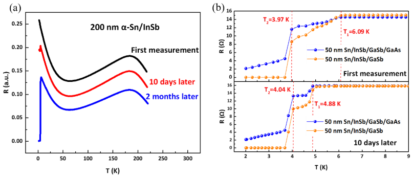
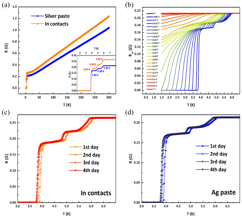
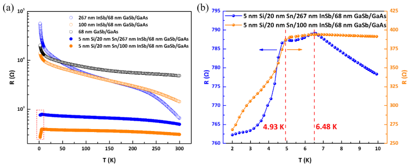
The central claim is that MBE-grown alpha-Sn films in the 20-400 nm thickness range, not just monolayer stanene, show multiple superconducting transitions. Besides a transition near 3.7 K attributed to beta-Sn inclusions, the films show sharp transitions at 4.96 K and near 6 K, with smaller volume fractions (below about 20 percent), higher critical fields, and stronger aging sensitivity. Control experiments rule out indium contacts, surface oxide, and the InSb template as the source, since Ag-paste contacts on the same sample reproduce all three transitions, silicon capping preserves them, bare templates show no superconductivity, and the transitions persist over days at low temperature. The authors interpret the higher-temperature transitions as superconductivity from phases of the strained alpha-Sn film itself, possibly connected to its topological band structure, while leaving indium-tin alloy formed during growth as an acknowledged alternative they have not yet ruled out.
Load-bearing premise
The new claim stands on the premise that the 4.5-6 K transitions are not caused by indium-tin alloy or another secondary phase formed during growth, which the authors state they have not yet observed or ruled out.
Editorial extensions
If this is right
- Superconductivity in alpha-Sn is not limited to few-layer stanene; films tens to hundreds of nanometers thick show transitions above the beta-Sn critical temperature.
- The higher-Tc transitions carry larger critical fields than the beta-Sn transition and show two-dimensional anisotropic field behavior, giving a clear transport signature to identify them.
- Strain from the InSb template stabilizes the alpha-Sn structure and suppresses the beta-Sn fraction, while the transition near 5 K persists, pointing to strain as a controlling parameter.
- Freshness matters: room-temperature aging affects the higher-Tc transitions far more than the beta-Sn transition, so time-controlled measurements are needed to characterize these phases.
- The possibility that strained alpha-Sn is a topological superconductor remains open, since the observed phases occur in the predicted topological regime.
Reading between the lines
- If the In-Sn alloy alternative is excluded by nanoscale composition mapping, the remaining explanation is an intrinsic superconducting phase of strained alpha-Sn, which would make the film a promising platform for searching for topological superconductivity.
- The incomplete transitions and the small 6.48 K feature interpreted as granular fluctuations suggest these phases may be filamentary; whether zero resistance is achieved may depend on percolation, so patterned or thinner samples might reveal different transition completeness.
- Because the high-Tc transitions age faster than the beta-Sn transition, a direct time-resolved correlation between lattice strain and superconducting critical temperature on the same sample would test whether strain relaxation is what kills the new phase.
Signed reviews
Editorial analysis
A structured set of objections, weighed in public.
Referee Report
Summary. The manuscript reports transport measurements on MBE-grown α-Sn films on InSb-based templates (type A and type B) with thicknesses from 20 to 400 nm. The authors observe multiple superconducting transitions: a β-Sn-like transition near 3.7 K and additional transitions at 4.5–6.5 K. They rule out pressed In contacts as the source by comparing with Ag paste contacts, rule out surface oxides by capping with Si, and show that bare InSb/GaSb/GaAs templates are not superconducting. They also characterize aging effects and magnetic field dependence, extracting critical fields and fitting the angular dependence to the Tinkham model, noting 2D character and a high in-plane critical field of about 0.82 T for the higher-Tc transition in a 50 nm sample. The authors propose that the higher-Tc transitions may come from α-Sn-related phases, but they explicitly acknowledge in the Discussion that In-Sn alloy formation at the α-Sn/InSb interface remains a possible source.
Significance. If the higher-Tc transitions are intrinsic to strained α-Sn films, the result would be significant for topological superconductivity and would extend previous stanene work to much larger thicknesses. The paper includes useful controls for contacts and oxidation, and the aging measurements provide a careful characterization of sample evolution. However, the central attribution is not yet established because In-Sn alloy formation at the α-Sn/InSb interface has not been excluded. The observations are interesting and meritorious, but the strength of the title and the claim that 'superconductivity in α-Sn thin films up to this thickness range has never been reported' exceed what the current evidence supports.
major comments (2)
- [Discussion, 'Another possible source...' and Figure 5] The In-Sn alloy scenario is not excluded and is load-bearing for the central claim. The Ag-paste control in Figure 3(a) rules out In contacts but not In that segregates from the InSb layer during growth or over time. The template measurements in Figure 5 lack the α-Sn/InSb interface and therefore do not address this possibility. Since In-Sn alloys have Tc values from 3.4 to 7.3 K (Refs. 29, 30) that bracket the observed higher-Tc transitions (4.5–6.5 K), and since the aging sensitivity of the higher-Tc transitions is qualitatively consistent with In diffusion, the statement in the Discussion that 'The superconductivity in α-Sn thin films up to this thickness range has never been reported' is not supported. The authors should provide direct evidence excluding interface In-Sn alloy formation—for example, EDX or electron energy-loss spectroscopy mapping across the interface, SIMS depth profiling, or a control film grown on an In-free substrate such as CdTe—or explicitly reframe the claim as 'superconducting transitions observed in α-Sn films whose origin remains to be identified.'
- [Figure 4 and equations (1)–(2)] The extracted critical fields lack uncertainty estimates and the fitting procedure is incompletely described. The paper states in the caption of Figure 4 that the critical field is decided at the field where the resistance reaches 90% of its value at 4 T, but the fits to Eq. (1) and the Tinkham model Eq. (2) are not reported with the fitted parameters (Bc⊥, Bc∥, Tc) and their errors. The in-plane critical field of 0.82 T for the higher-Tc transition is a key quantitative claim, and it should be accompanied by the full fit parameters and an uncertainty estimate so that it can be meaningfully compared with the critical fields of candidate secondary phases such as In-Sn alloys.
minor comments (5)
- [Method] The text contains placeholder question marks in 'out-of-plane residual strain(?)' and 'plastic flow model (?)' in the Method section; these should be replaced with proper terms and references.
- [Figure 2(b) caption] The caption says 'two type B samples grown on GaAs and GaSb substrates,' but the type B structure in Figure 1(a) uses GaAs substrates with GaSb and InSb buffer layers; the caption should be clarified to specify the actual difference between the two samples.
- [Results, Figure 4] The sentence 'The critical field increases with the angle of the magnetic field relative to the normal of the sample surface as shown in the inset of Figure 4(b)' is slightly ambiguous; explicitly stating that 0° is normal and 90° is parallel to the surface would improve readability.
- [Summary] The Summary states that 'Multiple transitions above 4 K with larger critical fields should come from other possible sources such as In contacts, In-Sn alloys or oxides,' which is inconsistent with the earlier Discussion statement that 'more than one superconducting phases exist in our α-Sn samples besides β-Sn'; the authors should make their attribution consistent throughout.
- [Method, growth details] The statement that 'The details about the growth and structural characterization are presented elsewhere' should include a citation or be expanded, since the growth quality and interface structure are important to the claims in the paper.
Circularity Check
No circularity: the superconducting transitions are directly measured, and the acknowledged In-Sn alloy possibility is an alternative explanation, not a self-referential construction.
full rationale
The paper is an experimental transport report rather than a derivation chain, so there is no claimed prediction that reduces by construction to its own inputs. The only quantitative quantity extracted from a formula is Bc(0) = 1360 Oe, obtained by fitting the measured temperature-dependent critical fields to the standard relation Bc(T) = Bc(0)[1 - (T/Tc)^2]. This is a post-hoc fit to the data, not a parameter that was fitted to one part of the data and then used to predict another closely related quantity. The central claims — multiple superconducting transitions above 4.5 K and their aging and strain behavior — are directly observed resistance anomalies with supporting controls: Ag-paste contacts reproduce the In-contact transitions, Si-capped samples show the same higher-Tc features, and template samples without α-Sn show no superconductivity. These are empirical checks, not circular definitions. The acknowledged possibility of In-Sn alloy formation from In segregation out of the InSb layer is a stated limitation and alternative explanation, not a circular step: the paper does not define the observed superconductivity in terms of the alloy, and no alloy-specific parameter is fitted and then renamed as a prediction. There is no load-bearing self-citation: the prior works cited are external experimental and theoretical results used for context or comparison (e.g., Didschuns on proximity effect, Liao/Xue on stanene). Therefore, whatever the correctness risk of the central claim, it is not a circularity risk.
Assumptions & free parameters
free parameters (3)
- Bc(0) for lowest-Tc transition (100 nm type B) =
1360 Oe
- Tc fit for lowest transition =
3.8 K
- In-plane critical field for highest-Tc transition at 2 K =
0.82 T
assumptions (4)
- domain assumption The α-Sn films are fully strained and stabilized by the InSb substrate.
- domain assumption The InSb template layers and GaAs substrates are not superconducting in the temperature range of interest.
- domain assumption Indium and Ag paste contacts do not contribute to the higher-Tc transitions despite In-Sn alloy formation potential.
- standard math Standard Bc(T) and Tinkham angular dependence formulas apply to these thin film superconductors.
Cite this review
Pith. "Pith review of Multiple Superconducting Transitions in {\alpha}-Sn Films Grown by Molecular Beam Epitaxy." pith.science (2026). https://pith.science/paper/3XZYRFDP
@misc{pith2026190803362,
  author       = {Pith},
  title        = {Pith review of: Multiple Superconducting Transitions in \alpha-Sn Films Grown by Molecular Beam Epitaxy},
  year         = {2026},
  howpublished = {\url{https://pith.science/paper/3XZYRFDP}},
  note         = {Machine review of arXiv:1908.03362}
}
read the original abstract
Gray tin, also known as {\alpha}-Sn, has been attracting research interest recent years due to its topological nontrivial properties predicted theoretically. The Dirac linear band dispersion has been proved experimentally by angle resolved photoemission spectroscopy. We have grown a series of {\alpha}-Sn thin film samples in two types with different substrates and thicknesses by molecular beam epitaxy. To explore the possible exotic physical properties related to the topological band structures, we have measured the electrical transport properties of our {\alpha}-Sn thin film samples and observed multiple superconducting transitions. We have identified the transitions above 4.5 K, besides the transition maybe related to the \b{eta} phase around 3.7 K. The changes of the superconducting properties over time reflect the aging effects in our samples. We have also confirmed the strain effects on the superconducting transitions through altering the relative thickness of our samples.
Figures

Figures from the paper (2 more)

Reference graph
Works this paper leans on
- [1]
-
[2]
A. W. Ewald and E. E. Kohnke, Physical Review 97, 607 (1955)
work page 1955
-
[3]
A. W. Ewald and O. N. Tufte, Journal of Applied Physics 29, 1007 (1958)
work page 1958
-
[4]
E. E. Kohnke and A. W. Ewald, Physical Review 102, 1481 (1956)
work page 1956
-
[5]
A. W. Ewald and O. N. Tufte, Journal of Physics and Chemistry of Solids 8, 523 (1959)
work page 1959
-
[6]
E. D. Hinkley and A. W. Ewald, Physical Review 134, A1261 (1964)
work page 1964
-
[7]
R. F. C. Farrow, D. S. Robertson, G. M. Williams, A. G. Cullis, G. R. Jones, I. M. Young, and P. N. J. Dennis, Journal of Crystal Growth 54, 507 (1981)
work page 1981
- [8]
Show all 31 references
-
[9]
Mason and B
B. Mason and B. R. Williams, Surface Science 273, L472 (1992)
1992
-
[10]
Barfuss et al., Phys Rev Lett 111, 157205 (2013)
A. Barfuss et al., Phys Rev Lett 111, 157205 (2013)
2013
-
[11]
Y. Xu, B. Yan, H. J. Zhang, J. Wang, G. Xu, P. Tang, W. Duan, and S. C. Zhang, Phys Rev Lett 111, 136804 (2013)
2013
-
[12]
S. C. Wu, G. Shan, and B. Yan, Phys Rev Lett 113, 256401 (2014)
2014
-
[13]
Huang and F
H. Huang and F. Liu, Physical Review B 95 (2017)
2017
-
[14]
Zhang, H
D. Zhang, H. Wang, J. Ruan, G. Yao, and H. Zhang, Physical Review B 97 (2018)
2018
-
[15]
C. Z. Xu et al., Phys Rev Lett 118, 146402 (2017)
2017
-
[16]
Ohtsubo, P
Y. Ohtsubo, P. Le Fevre, F. Bertran, and A. Taleb -Ibrahimi, Phys Rev Lett 111, 216401 (2013)
2013
-
[17]
J. C. Rojas-Sanchez et al., Phys Rev Lett 116, 096602 (2016)
2016
-
[18]
M. R. Scholz et al., Physical Review B 97 (2018)
2018
-
[19]
Liang, Q
T. Liang, Q. Gibson, M. N. Ali, M. Liu, R. J. Cava, and N. P. Ong, Nat Mater 14, 280 (2015)
2015
-
[20]
Xiong, S
J. Xiong, S. K. Kushwaha, T. Liang, J. W. Krizan, M. Hirschberger, W. Wang, R. J. Cava, and N. P. Ong, Science 350, 413 (2015)
2015
-
[21]
Feng et al., Physical Review B 92 (2015)
J. Feng et al., Physical Review B 92 (2015)
2015
-
[22]
Shaidu and O
Y. Shaidu and O. Akin-Ojo, Comp Mater Sci 118, 11 (2016)
2016
-
[23]
F. F. Zhu, W. J. Chen, Y. Xu, C. L. Gao, D. D. Guan, C. H. Liu, D. Qian, S. C. Zhang, and J. F. Jia, Nat Mater 14, 1020 (2015)
2015
-
[24]
Liao et al., Nature Physics 14, 344 (2018)
M. Liao et al., Nature Physics 14, 344 (2018)
2018
-
[25]
Tinkham, Physical Review 129, 2413 (1963)
M. Tinkham, Physical Review 129, 2413 (1963)
1963
-
[26]
Didschuns, K
I. Didschuns, K. Fleischer, P. Schilbe, N. Esser, W. Richter, and K. Lü ders, Physica C: Superconductivity 377, 89 (2002)
2002
-
[27]
Didschuns, Physica B: Condensed Matter 284-288, 1121 (2000)
I. Didschuns, Physica B: Condensed Matter 284-288, 1121 (2000)
2000
-
[28]
A. M. Toxen, M. J. Burns, and D. J. Quinn, Physical Review 138, A1145 (1965). [29]J. H. Wernick and B. T. Matthias, The Journal of Chemical Physics 34, 2194 (1961)
1965
-
[30]
M. F. Merriam and M. Von Herzen, Physical Review 131, 637 (1963)
1963
-
[31]
Allain, Z
A. Allain, Z. Han, and V. Bouchiat, Nat Mater 11, 590 (2012)
2012
-
[32]
Y. Sun, H. Xiao, M. Zhang, Z. Xue, Y. Mei, X. Xie, T. Hu, Z. Di, and X. Wang, Nat Commun 9, 2159 (2018). Figure 1. Schematic layer structures and XRD patt erns for two type α-Sn samples. (a) Sample structures for two type samples. Type A: α-Sn thin films grown on InSb substrat...
2018
Reviewed August 14, 2026 · model on record in the stance chip above.
Discussion (0). Continue with ORCID to comment.